 |
||
|
||
| ||
|
||
|
||
| ||
Not willing to wait until AMD releases more high-end solutions, NVIDIA has decided to stage a preemptive strike by releasing an overhauled GPU based on the improved Fermi architecture. It would seem that the novelty was ready for some time and NVIDIA was just waiting for a good moment to unveil it. NVIDIA had the fastest graphics card anyway and there was no sense in competing with own products. But when it became clear that AMD was going to unveil a more powerful solution, there were no reasons to delay the release of GF110, NVIDIA needed to show what they were capable of, and foil rival's plans as well. So today, about a year after the release of GeForce GTX 480 based on GF100, the company announced the new GeForce GTX 580. NVIDIA calls GeForce GTX 580 the fastest DirectX 11 solution, and it is where single-GPU cards are involved, because the dual-GPU Radeon HD 5970 can still occasionally outperform GTX 580 even in DX11 games. So GeForce GTX 580 continues what GTX 480 started, offering more performance and efficiency, having lower power consumption and quieter cooler. The new GPU was designed for higher power efficiency and all architectural changes are aimed at improving performance at reduced power consumption. But you cannot say that GF110 is just a revision of GF100, because there are certain hardware changes as well. The key difference of the new GPU is that it has more active (i.e. enabled by default) execution units like stream processors and tessellation units, as well as higher clock rates at lower power consumption and quieter cooler. Besides, a number of architectural changes are related to texturing and z-cull algorithm which improve performance of the new GPU over GF100 even at the same clock rates. In general, the novelty is a second edition, revised and enlarged. A truly full-fledged Fermi with all execution units enabled. So how did NVIDIA manage to seriously improve its top-end products? Firstly, TSMC had mastered the 40nm process technology by the autumn and thus improved the yield of good chips. Secondly, they overhauled the GPU to optimize power consumption and make it capable of working at higher clock rates, something that GF100 had certain problems with. This theoretical part will be brief, because GF110 (GTX 580) is similar to GF100 (GTX 470 and GTX 480), and certain architectural modifications resemble those of GF104 (GTX 460), differences being quantitative. Since we have already described the Fermi architecture in detail, you might want to read the following reviews, as well as revise information on NVIDIA architectures from GeForce 8800 GTX on.
Now let's take a close look at the specifications of the GF110 GPU and the GeForce GTX 580 graphics card. GeForce GTX 580 graphics card
Reference GeForce GTX 580 specifications
The new GF110, as well as GeForce GTX 580, are called to gradually replace GF100 and GTX 480. Like the latter, the new GPU is also made using the 40nm process technology. While NVIDIA didn't change its product naming policy, it still named the novelty GTX 580, which would normally mean a new generation of products. But we believe it would've been more logical to name the chip GTX 485 (similar to GTX 285), because GF110 doesn't have any radical architectural changes. Yes, it's been overhauled, but the functional differences from GF100 are still not enough to consider GF110 a new-generation solution. But as you know, product naming is handled by marketing departments. It isn't based on actual capabilities often. Only one graphics card, GeForce GTX 580, is currently available on GF110. NVIDIA hasn't yet announced the long-anticipated GTX 570. Well, they need to sell remaining GTX 470 and GTX 480, don't they? The suggested retail price of $499 (without taxes) is quite predictable and expected. Like the preceding GTX 480, the novelty has the 384-bit memory bus and the corresponding memory volume of 1536MB. This seems like the only reasonable number, because 768MB would've been insufficient and 3GB would've been too much. Even considering that the rival are going to release a 2GB solution, 1536GB should be enough for all modes. Adding another 1.5GB just wouldn't be justified economically. GF110 architectureThe GF110 was overhauled to improve the performance/consumption ratio. Every unit of it was modified to a certain extent. Of course, NVIDIA wouldn't provide a complete list of changes, but they claim that most transistors have been remade. GF110 features the same Stream Multiprocessors with the same amount of CUDA cores per each as GF100 does. In terms of architecture, the new GPU is similar to GF100. It has the same multiprocessor configuration, consists of Graphics Processing Clusters, each of which includes several Stream Multiprocessors, each of which includes several stream processors. 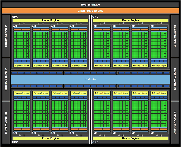 GF110 features 8 GPCs, 16 SM and 6 x 64-bit memory controllers connected to an L2 cache and featuring 8 ROPs per each. The GPU has 512 stream processors in total, which are organized into 16 Multiprocessors. Unlike GeForce GTX 480, GeForce GTX 580 has all of them enabled by default. The memory subsystem has remained the same. Each multiprocessor has 64KB of on-chip memory that can be configured as either 48KB shared memory plus 16KB L1 or, vice versa, 16KB shared memory and 48KB L1. Besides, GF110 has 768KB of unified L2 that serves all requests for loading and storing data as well as texture fetches. As for architectural changes, GF110 has one performance indicator that has been doubled. It's not the number of TMUs as it was once rumored. If you remember how the Fermi architecture was changed in GF104, you might have probably guessed that the today's novelty can also process texture data in any format up to FP16 (bilinear filtering included) at full speed. Just to remind you, GF100 cannot do that. It's theoretical speed of processing FP16 textures (which are often used in modern games) is twice as lower than those of GF104 and GF110. This improvement can help increase rendering performance in many applications that use off-screen buffers, e.g. HDR rendering. This modification also explains early rumors about those 128 TMUs in GF110. The second architectural difference is of somewhat lower importance. The GPU has the improved z-cull algorithm, for which new tile formats have been introduced. This change is called to improve performance in certain situations, and we'll check that in our synthetic tests. In general, architectural changes alone resulted in a 5-10% performance boost, according to tests conducted by NVIDIA. In some applications, like DiRT 2 and 3DMark Vantage, the boost reaches 15%.  Compared with GF100, the increased number of active execution units, working at higher clock rate and consuming less power, adds another 10-15%, so the average rendering performance boost of GTX 580 vs. GTX 480 should be about 20%. This is very nice, considering the few architectural changes. But we'll see if this all is true in our tests. Write a comment below. No registration needed!
|
Platform · Video · Multimedia · Mobile · Other || About us & Privacy policy · Twitter · Facebook Copyright © Byrds Research & Publishing, Ltd., 1997–2011. All rights reserved. |


