NVIDIA Editor's Day, October 2007
NVIDIA Editor's Days are usually very informative and interesting events. The date of the Editor's Day, to be held in Santa Clara, as usual, was put off several times. iXBT.com might have even lost the chance of taking part in this event, because our reporter couldn't get the American visa until the very end. Eight hours prior to departure, everything was finally settled, and after twenty hours of the flight and airports we reached our destination.
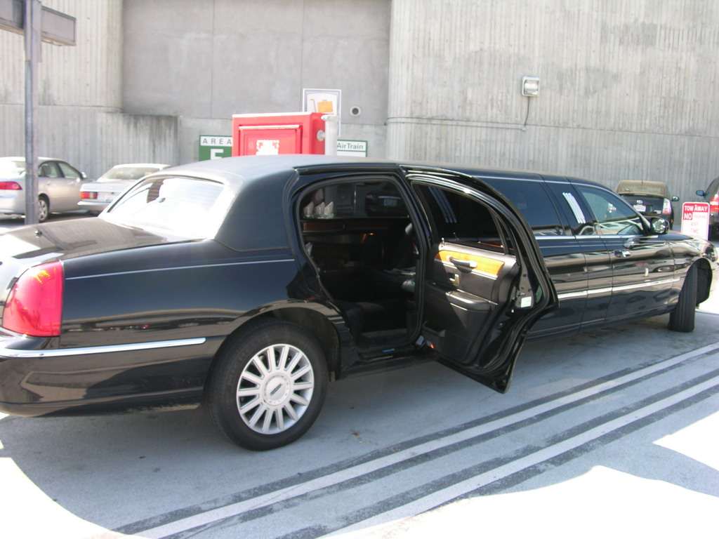
The flight across 11 time zones, lift-offs and landings, and packed meals were spiced up with a luxurious long Lincoln and a polite driver, who delivered our tired iXBT.com editor to the hotel.
Such hospitality is a common practice for NVIDIA Editors Day in California. But I was surprised to see this original car, fit for a wedding.
California met me with the mild warm sun. The problem with forest fires in the South part of the state had no effect on San Francisco and Santa Clara.
Early in the morning, many editors gathered at the table to get their badges. Representatives of European media suffered from the time lag - their fellow countrymen were finishing their working day, some of them were already going to bed.
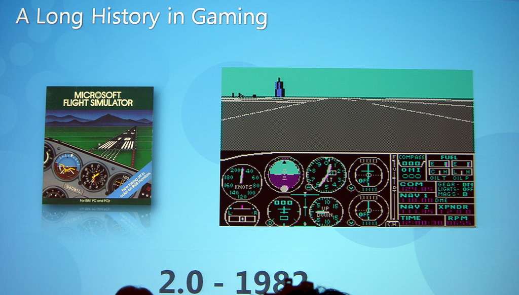
After a luncheon we were already listening to the first speaker, a Microsoft representative. The lively man (Kevin Unangst) decided to demonstrate the evolution of computer games for Windows by the example of Microsoft Flight Simulators.
 A touching label on the box with the second version of Flight Simulator:
"Now taking off in color on RGB monitors".The latest generation of Microsoft Flight Simulator X Accelerator with DirectX 10 support is certainly a huge step forward since 1982. A screenshot of this game looks like a photo: natural shadows, smooth lines, impressively realistic looking water. It's possible even now, but under one condition: your system must support DirectX 10 for such games. Moreover, not a single modern game console is fast enough to reach this level of image quality and realism in games. That's the only way to enjoy all features of modern 3D games... At least, that's what the Microsoft representative told us.
Kevin demonstrated a slide to support his words. According to this slide, PC games sales tripled in last decade, and Windows Vista is the fastest selling software product in history. Vista and DX10 will be supported by 15M GPUs sold by end of 2007. Their number will grow to 102M by end of 2008.
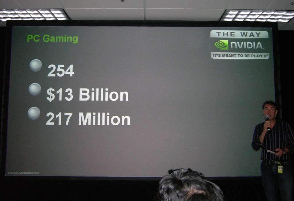
Roy Taylor, NVIDIA's Vice President echoes Microsoft. He's responsible for creating new content to be used by modern hardware projects in this company.
His words were supported with even more impressive numbers: 254 games were launched since the campaign - The way NVIDIA: It's meant to be Played.
The total game sales yielded $13 billions, 217 million people play online games now.
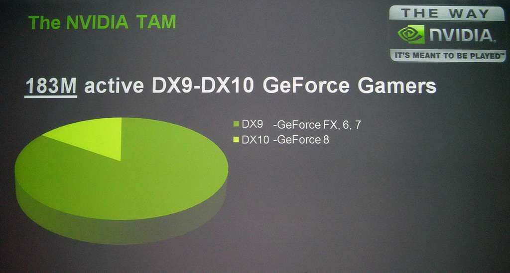
There are 183 millions of active NVIDIA gamers.
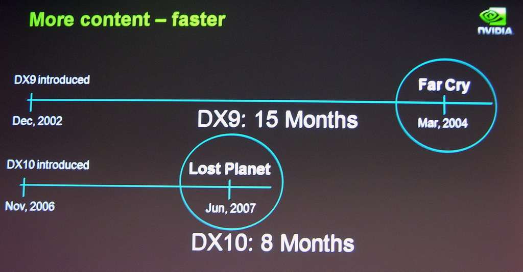
According to Taylor, DirectX 10 allows to create new content almost twice as fast. For example, it took a real DirectX 9 game over a year to appear after DirectX 9 had been launched in December 2002. And the first DirectX 10 version of Lost Planet has been launched in eight months, in June.
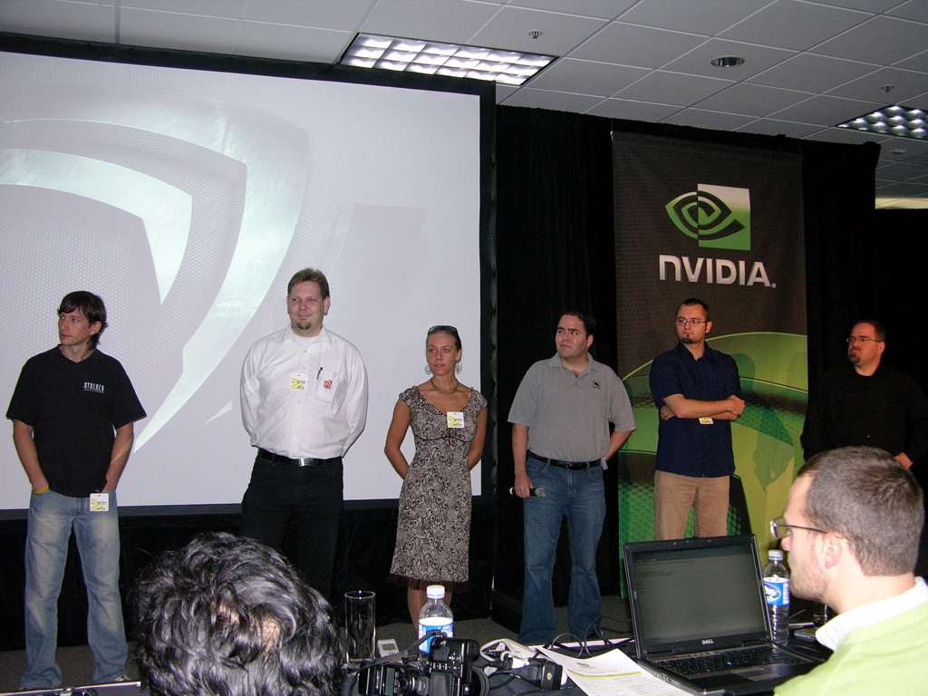
We've heard a lot about DirectX 10 effects. The following developers were in the group that helped NVIDIA demonstrate them - Irina Semenova (Akella, Russia), Oleg Iavorsky (GSC, Ukraine), Ingo Horn and Pavel Miechowski (Metropolis, Poland), as well as Fernando Paiz and Adam Mersky (Turbine, USA).
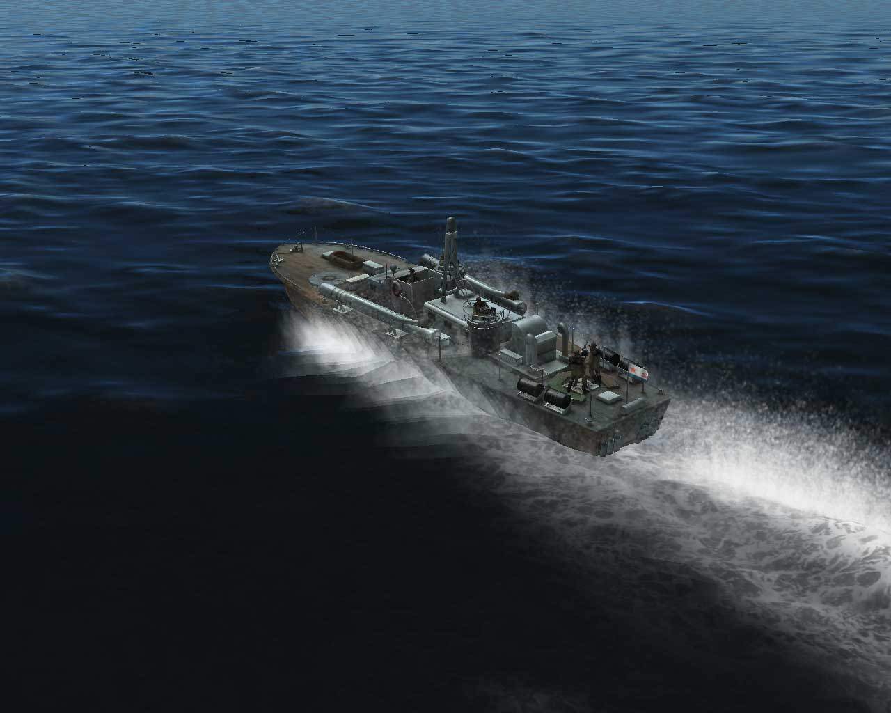
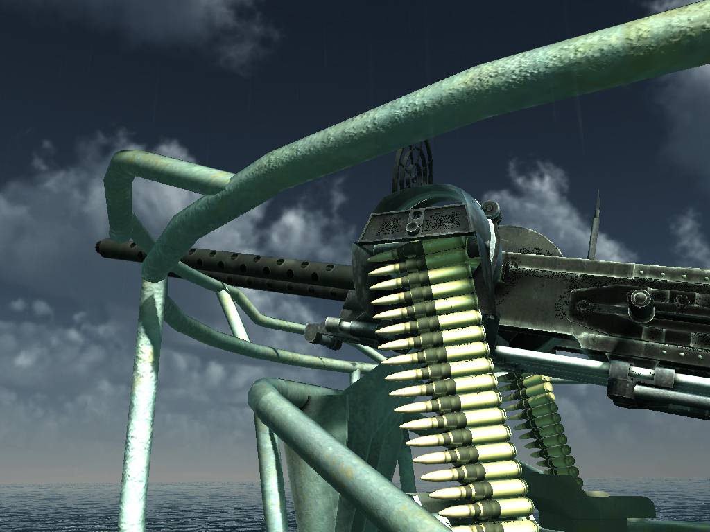
Akella demonstrated a naval strategy game "PT Boats: Knights of the Sea".
GSC Proved the power of DX10 with "S.T.A.L.K.E.R.: Clear Sky", which is still in development.
Their Polish colleagues from Warsaw impressed us with their new first-person shooter THEY featuring a lot of effects.
American developers demonstrated the recent beta implementation of DirectX 10 support in The Lord of the Rings Online MMORPG.
After this massive assault on our minds, none should have any doubts that only DX10 technologies can provide necessary image quality in games. The required minimum is the GeForce 8800GT, to be described below.
Before we proceed to the main feature of our review, we'd like to note that NVIDIA employees focus not only on modern high-performance GPUs. They also offer complex solutions for hardcore (and common) gamers. It's too early to speak about some things now. Some of them can be only whispered. We can only say that the P35 and X38 chipset will have a decent match soon. Along with support for DDR3 and modern processors from Intel, NVIDIA will offer a new SLI level to support traditional and quad SLI configurations as well as triple SLI.
Running further forward, we can also say that computer enthusiasts in opposition will also find a good option to upgrade their platforms.
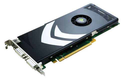
And now let's get back to the present: meet a new price/performance leader - GeForce 8800GT.
Theory and architecture
In our article devoted to the new Mid-End GPUs of the NVIDIA G8x family we complained that these Mid- and Low-End solutions were cut down too much (ALUs and TMUs), and failed to demonstrate the expected performance level. Besides, even the Upper Mid-End product is not equipped with a 256-bit memory bus. We also expressed our concern that the new graphics cards would demonstrate relatively weak results in modern games and that DirectX 10 would not help them. We were right. Low-end and mid-end products of the G8x family demonstrated their weakness.
And now, six months after the announcement of the G84 and corresponding solutions, a new GPU is released - G92. The first graphics cards with this GPU are designed for the Upper Middle segment, from $200 to $250. This very GPU has been used in the most powerful Mid-End cards, which brought a 256-bit memory bus into this price segment as well as quite a lot of unified processors. So, today we shall meet an overhauled mid-end solution from NVIDIA based on the updated G9x unified architecture.
Before you read this article, you should look through the baseline theoretical articles - DX Current, DX Next, and Longhorn. They describe various aspects of modern graphics cards and architectural peculiarities of products from NVIDIA and AMD (former ATI).
These articles predicted the current situation with GPU architectures, many of our assumptions came true. Detailed information about the unified NVIDIA G8x architecture of older chips can be found in the following articles:
We must warn you that this review will be incomplete, NVIDIA is reluctant to give away all details about its new GPUs and cards. For example, we don't know for sure whether this GPU supports new features unavailable in the G8x (for example, Shader Model 4.1 and FP64 for CUDA and other applications). We cannot explain such secrecy - whether the company is being cautious before corresponding solutions are launched by the only competitor, or NVIDIA is just too relaxed. Or perhaps the G9x title implies only the new process technology, although similar updates (or even grander GPU changes) used to be included into the same family, for example, G71 or NV35.
Architecture of the overhauled GPU is based on the GeForce 8 (G8x). The G92 GPU features all advantages of the G8x, such as the unified shader architecture, full support for DirectX 10, high quality methods of anisotropic filtering, and a new CSAA algorithm with up to 16 samples. Some units are improved compared to the G80. The G92 is currently planned to be used in graphics cards for $199-$249, that is in the Mid-End price segment. The key change is the 65 nm process technology, which allows to reduce the cost, which is very important for relatively inexpensive products. It may be this finer technology that brings our solutions to this price segment.
GeForce 8800 GT
- Codename: G92
- Process technology: 65 nm
- 754 million transistors (more than in the G80)
- Unified architecture with an array of common processors for streaming processing of vertices and pixels, as well as other data
- Hardware support for DirectX 10, including Shader Model 4.0, geometry generation, and stream output
- 256-bit memory bus, four independent 64-bit controllers
- Core clock: 600 MHz (GeForce 8800 GT)
- ALUs operate at more than a doubled frequency (1.5 GHz for the GeForce 8800 GT)
- 112 (in the GeForce 8800 GT, probably 128 in total) scalar floating-point ALUs (integer and floating-point formats, FP32 support within the IEEE 754 standard, MAD+MUL without penalties)
- 56 (64) texture units supporting FP16 and FP32 components in textures
- 56 (64) bilinear filtering units (as in the G84 and G86, no free trilinear filtering and more efficient anisotropic filtering)
- Dynamic branches in pixel and vertex shaders
- 4 (6) wide ROPs (16 pixels) supporting antialiasing with up to 16 samples per pixel, including FP16/FP32 frame buffer formats. Each unit consists of an array of flexibly configurable ALUs and is responsible for Z generation and comparison, MSAA, blending. Peak performance of the entire subsystem is up to 64 MSAA samples (+ 64 Z) per cycle, 128 samples per cycle in Z only mode
- 8 multiple render targets (MRT)
- All interfaces are integrated in the GPU (2 x RAMDAC, 2 x Dual DVI, HDMI, HDTV), unlike the external NVIO chip in the GeForce 8800
The first G92-based graphics cards
Specifications of the Reference GeForce 8800 GT 512MB
- Core clock: 600 MHz
- Frequency of unified processors: 1500 MHz
- Unified processors: 112
- 56 texture units, 16 blending units
- Effective memory clock: 1.8 GHz (2*900 MHz)
- Memory type: GDDR3
- Memory: 512 MB
- Memory bandwidth: 57.6 GB/sec.
- Maximum theoretical fillrate: 9.6 gigapixel per second.
- Theoretical texture sampling rate: up to 33.6 gigatexel per second.
- Power consumption: up to 110 W
- 2 x DVI-I Dual Link, 2560x1600 video output
- SLI connector
- PCI Express 2.0
- TV-Out, HDTV-Out, HDCP support
- Recommended price: $249
Specifications of the Reference GeForce 8800 GT 256MB
- Core clock: 600 MHz
- Frequency of unified processors: 1500 MHz
- Unified processors: 112
- 56 texture units, 16 blending units
- Effective memory clock: 1.4 GHz (2*700 MHz)
- Memory type: GDDR3
- Memory size: 256 MB
- Memory bandwidth: 44.8 GB/sec.
- Maximum theoretical fillrate: 9.6 gigapixel per second.
- Theoretical texture sampling rate: up to 33.6 gigatexel per second.
- Power consumption: up to 110 W
- 2 x DVI-I Dual Link, 2560x1600 video output
- SLI connector
- PCI Express 2.0
- TV-Out, HDTV-Out, HDCP support
- Recommended price: $199
As you can see, there are plans to manufacture the GeForce 8800 GT in two modifications, which will differ in video memory size and its frequencies, and consequently in memory bandwidth. Memory of a more expensive product with 512 MB of local video memory to be the first on the market will operate at 1800 MHz. Memory clock rate of the second modification will be only 1400 MHz. The product with less memory will appear in stores later, such products will be manufactured by some of NVIDIA partners. The GeForce 8800 GT must reinforce positions of the GeForce 8600 and prolong the line of successful Mid-End solutions from NVIDIA, the most popular products.
It's very important to digress to the topic of video memory size required by modern games. Our recent analysis has shown that the latest games have high video memory requirements, they use up to 500-600 MB of memory. It does not mean that all game resources must be stored in local memory of a graphics card. Resources may often be managed by the API, especially as Direct3D 10 uses video memory virtualization. Nevertheless, modern 3D applications tend to require increasing volumes of local video memory. 256 MB of memory is now the minimum memory size. An optimal parameter is currently 512 MB. You must take it into account, when you choose between these two modifications of the GeForce 8800 GT.
Architecture
The information provided by NVIDIA does not tell us whether the G92 differs from the G8x on the architectural level. We can only assume that the G92 is the flagship of the G80 family manufactured by the new process technology with minor changes. It's much better than the previous G84 processor, which is actually 1/3 or 1/4 of the G80. According to NVIDIA, the GPU has seven big shader units (56 TMUs) as well as four wide ROPs. The number of transistors suggests that the company is hiding something. It's quite possible that the solutions announced today do not use all physically available units, and the G92 has more units than the GeForce 8800 GT uses. However, higher complexity of the GPU can be explained by NVIO and a new-gen video processor, which are now incorporated into the GPU.
This time NVIDIA decided to retain quite a lot of units in its mid-end GPU to compete well with future AMD products. Our assumption made in the G84 and G86 reviews that the 65 nm technology would be used in much faster GPUs for the Mid-End segment is proved now. Later on we shall benchmark the new GPUs in synthetic and game tests. But even now we can say for sure that G92-based solutions will be very fast owing to many ALUs, TMUs, ROPs, and good memory bus throughput.
The G92 does not have many architectural changes. We shall not dwell on them, because according to NVIDIA, there are no changes compared to the G8x. Everything we wrote in reviews of the previous GeForce 8 solutions holds good. We'll only repeat some key points about architectural specifications of the new GPU.
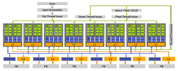
As you may remember, the diagram of the unified G80 looks like this:
NVIDIA publishes the following diagram of the new solution in its briefs:
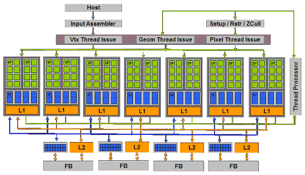
That is the only change is fewer units. As we have mentioned above, we doubt that it's physically true, but our description is based on the information provided by NVIDIA. G92 consists of seven unified processors, NVIDIA traditionally speaks of 112 processors (at least in the first GeForce 8800 GT solutions). Each block consists of eight TMUs and sixteen ALUs. It can execute a part of a vertex, pixel, or geometry shader over a block of 32 pixels, vertices, or other primitives. It can compute other (nongraphical) tasks. Each processor has its L1 cache to store textures and other data. Along with the thread processor and shader processors, there are four ROPs that compute visibility, write data into a frame buffer, and do MSAA, grouped with memory controllers, write queues, and L2 Cache.
Unified processors and TMU
The diagram of shader units and the analysis of their peak computing capacity in the G80 were published in the corresponding article. It hasn't changed in the G92. It's easy to recalculate their performance using the modified clock rate. ALUs operate at more than the double frequency. They are scalar units, which helps achieve high efficiency. We don't know about functional differences, whether this GPU can do FP64. They certainly support computing in integer format. They comply with the IEEE 754 standard, important for scientific, statistical, economic, and other computations.
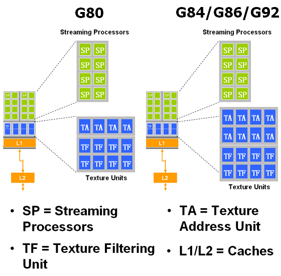
Texture units in the G92 differ from those in the G80. They copy the TMUs used in the G84 and G86, which architecture was modified to increase performance. You may remember that each texture unit in the G80 can compute four texture addresses and execute eight texture filtering operations per cycle. And G84/G86 TMUs can do twice as many texture fetches. That is each unit now has eight texture address units (TA) and just as many texture filtering units (TF):
We'll check it up in the practical part by analyzing results of synthetic tests. The other functions of texture units have not been changed, the GPU supports FP16/FP32 texture formats, etc.
ROPs, frame buffer, antialiasing
ROPs have not been changed either, but their number changed. The G80 has six ROPs, while the new solution has four of them to reduce the manufacturing costs of GPUs and PCBs. This reduction may also have to do with the objective to ease down competition with the existing top solutions.
Each unit processes four pixels (16 subpixels). So we've got 16 pixels per cycle for color and Z. Twice as many samples are processed per cycle in Z only mode. The GPU can process two pixels per cycle in MSAA 16x mode, in 4x mode - 8 pixels, etc. Like G80, the new GPU has full support for FP32/FP16 frame buffer formats together with antialiasing.
A new antialiasing method is supported - Coverage Sampled Antialiasing (CSAA). We've already seen it in previous GPUs of the family, and it was described in detail in the corresponding article:
In brief, color and Z values of samples are stored separately from information about their location. There can be up to 16 samples and just 8 Z values per pixel - it saves bandwidth and cycles. CSAA allows to do with transmitting and storing a single color value or Z value per each subpixel. It specifies more accurately the averaged value of a screen pixel by using precise information how this pixel covers triangle borders. As a result, the new method performs 16x antialiasing of noticeably higher quality than MSAA 4x, and the computing expenses are not very high.
One more innovation - the GeForce 8800 GT has an updated transparency antialiasing algorithm. A user could choose one of two options: multisampling (TRMS) and supersampling (TRSS). The former was very fast, but it was not efficient in all games. The latter offered higher quality, but it was slow. The GeForce 8800 GT is said to have a new method of transparency multisampling with improved quality and performance. This algorithm improves quality almost like supersampling. But it's very fast - it's just several percents slower than the mode without transparency antialiasing.
PureVideo HD
One of the expected changes in the G92 is the built-in video processor of the second generation, known by the G84 and G86, with advanced support for PureVideo HD. We already know that this video processor offloads a CPU almost completely when decoding all types of video data, including "heavy" H.264 and VC-1 formats.
Like the G84/G86, the G92 uses a new model of the programmable PureVideo HD processor, which includes the so called BSP engine. The new processor can decode H.264, VC-1, and MPEG-2 formats with the resolution of up to 1920x1080 and the bitrate of up to 30-40 Mbit/s. It does all the work of decoding CABAC and CAVLC data on the hardware level, so you can play all existing HD-DVD and Blu-ray discs even on mediocre single-core PCs.
You can read about the video processor of the second generation in the G84/G86 review. As for this article, we'll publish a diagram that illustrates the differences in hardware support for decoding video in various GPUs:
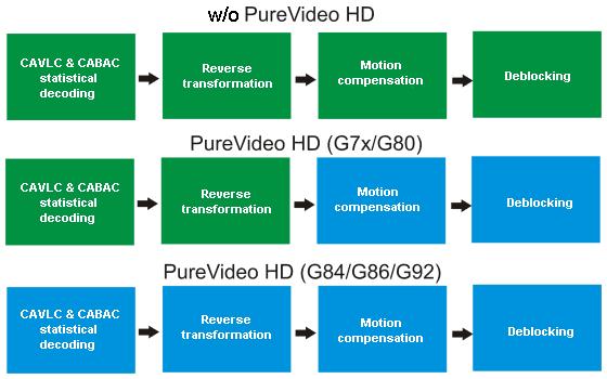
Tasks performed by a GPU are marked blue, green tasks are performed by a CPU. The old GPUs offloaded CPU only in some of the tasks. The new video processor in the latest NVIDIA GPUs performs these tasks on its own. We tested some of modern video solutions in the latest article devoted to evaluating efficiency of hardware-assisted video decoding.
PCI Express 2.0
What concerns truly new features of the G92, we can mention PCI Express 2.0. The second version of the PCI Express bus doubles the standard throughput, from 2.5 Gbps to 5 Gbps. As a result, the x16 slot can transfer data at up to 8 GB/s in each direction, unlike the 1.x version with its 4 GB/s. Most importantly, PCI Express 2.0 is compatible with PCI Express 1.1 - old graphics cards will work in new motherboards, and new graphics cards supporting the second version will also work in old motherboards. Provided the external power supply is sufficient. The interface bandwidth will not be increased, of course.
To provide backward compatibility with existing PCI Express 1.0 and 1.1 solutions, Specifications 2.0 support both transfer rates - 2.5 Gbps and 5 Gbps. Backward compatibility of PCI Express 2.0 allows to use old 2.5 Gbps solutions in 5.0 Gbps slots. They will work at lower speed. Devices designed in compliance with Specifications 2.0 can support both speeds - 2.5 Gbps and 5 Gbps. In practice, the situation with compatibility is good. But theoretically, there may be problems with some configurations (a motherboard plus expansion cards).
Support for external interfaces
The NVIO chip supporting external interfaces in the GeForce 8800 (2 x 400 MHz RAMDAC, 2 x Dual Link DVI (or LVDS), HDTV-Out) has been integrated into the GPU in this case. Support for the above-mentioned interfaces is built into the G92.
The GeForce 8800 GT cards are usually equipped with two Dual Link DVI-I connectors supporting DHCP. What concerns HDMI, this connector is fully supported. Manufacturers may implement it in cards of special design, which may appear a tad later. The card can do fine without the HDMI connector though, because it can be replaced with the DVI-HDMI adapter that comes with most modern graphics cards.
Unlike the AMD RADEON HD 2000, the GeForce 8800 GT does not contain a built-in audio chip required to transfer audio via DVI and the HDMI adapter. This feature to transfer video and audio signals via the same connector is popular in Mid- and Low-End cards, which are installed into small media centers. The GeForce 8800 GT will hardly be used in this role.
The practical part of the article will be published a tad later, because we got our GeForce 8800 GT too late. It will deal with the question how much the new solution from NVIDIA differs from previous cards and competing products.
Write a comment below. No registration needed!