 |
||
|
||
| ||
|
||
|
||
| ||
Part 1: Theory And Architecture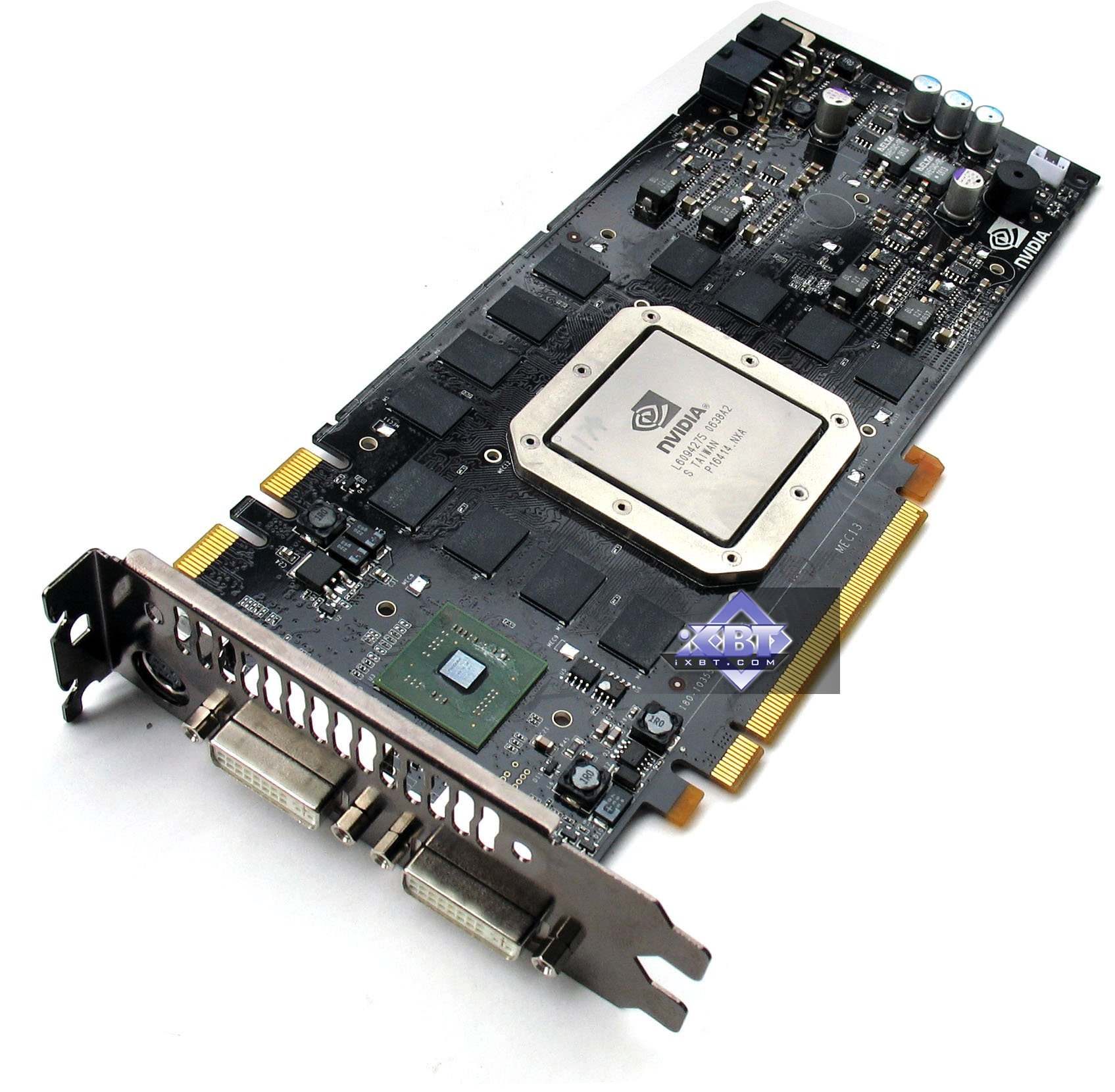
It's late autumn, it's danky and sometimes frosty... But this gloomy season is traditionally adorned by preparations to Christmas sales and holidays. It's also a tradition for vendors to release new products, so everyone can purchase them and provide companies with 90% of their annual income in just two months. Such announcements are usually made in October, so there's time to fill the stock and launch sales. And though NVIDIA dated the release to November 8, it began shipments two weeks earlier, so cards are available early in November (overpriced naturally). The market will establish the price, according to the demand however. Given its high, prices will correspond. Many of you experienced in 3D graphics heard enough about DirectX 10. This fundamentally new API, a part of MS Windows Vista, is to provide game and hardware developers with more flexibility and more opportunities. Actually such slogans preceed every new version, but seemingly all previous releases were not flexible and powerful enough, since they had to enter the field of unified processors and shaders. But more on that will be provided by Alexander Medvedev, our experienced veteran and guru of shader computing. It's obvious that 3D graphics with its performance and capabilities start with a GPU. And today we have the newest addition: GeForce 8800 GTX (formerly codenamed 'G80' and 'NV50'). 
That's how the wafer looks. An experienced user will notice that crystals are very large. That's because the new core has 681 million transistors! It's even much more than in any of Intel's high-end quad-core processor! Besides, NVIDIA's new product actually revolutionizes several design aspects. For starters, it introduces the 384-bit memory bus (intermediate between 256 and 512 bits), which dictates the memory capacity of 768 MB; supports the unified shader architecture, so there's no more vertex and pixel shader units (this will flourish in DX10 applications).  And now Alexander Medvedev will tell us about all architecture innovations in detail: The transition to unified graphics architectures has been long anticipated. Now we can state that GeForce 8800 arrival ('G80' for short) made it happen and the critical point had been passed. In the future these architectures will gradually descend to the middle- and low-end segments and will eventually converge with multi-core processor architectures. For starters, here are some links to revise the theory:
Now, let's get started! 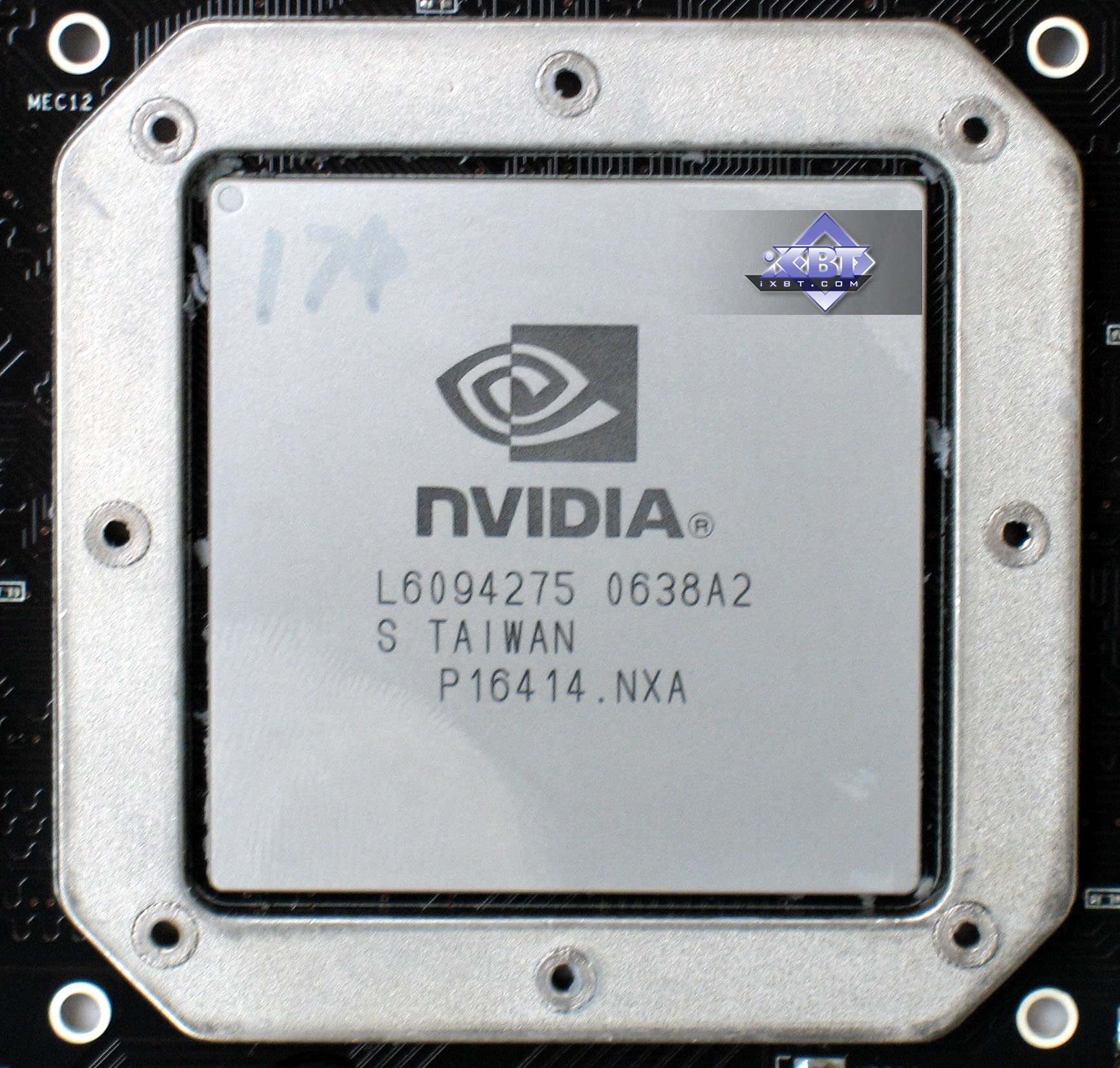
GeForce 8800 Graphics Accelerator
First cards based on GeForce 8800
ArchitectureSo, let's welcome NVIDIA's first unified architecture: 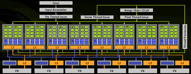
Here's the entire chip chart. The chip itself consists of 8 unified shader processors. NVIDIA claims there are 128 of them, declaring each ALU a processor. But that is somewhat incorrect, since a single command execution unit features 4 TMUs and 16 ALUs. This gives us total of 128 ALUs and 32 TMUs, but the granularity makes 8 units, each of which can be assigned a separate task, like executing parts of vertex or pixel or geometry shader on a 32-pixel unit (or a unit with corresponding number of vertices and other primitives). All branching, transitions, conditions, etc. are applied to the same unit, so it would be logical to call it shader processor in spite of its width. Each of these processors has its own L1 cache that keeps not only textures, like it was before, but other data that a shader processor might need as well. It's important to understand that primary data flow (like pixels and vertices) that is processed under the management of the "power broker" marked as 'Thread Processor', is not cached, but is streaming. This is the key peculiarity of modern graphics architectures - the absence of purely random access on the level of processed primitives. This might change in the future, but we'll return to that later. Besides the managing unit and 8 shader processors, there are 6 ROPs handling the visibility, frame buffer writes and MSAA (blue ones located near L2 units). These are grouped with memory controllers, write queues and L2 cache. Thus we get a very wide architecture (8 processing units, 32 pixels each) that is capable of smooth scalability in both ways. Adding or removing memory controllers and shader processors will correspondingly scale the throughput of the ENTIRE system without affecting the balance (remember ATI's key middle-end problem) and creating bottlenecks. Such a logical and beautiful solution that realizes the primary benefit of a unified architecture - automatic balancing and high resource usage efficiency. Half the units and you'll get a mid-end solution. Leave 2 shader processors and 1 ROP, and you have a value card that can also be integrated into chipsets. Besides shader units and ROPs, there is a set of managing units:
A little digression: obviously in the future these units will become more general and won't be related to specific shaders. They will become universal units handling data execution and format conversion (from one shader to another, from vertex to pixel, etc.) This won't introduce any fundamental changes into architecture, so this chart will look and work nearly the same, except for the fewer amount of special "grey" units. Already now all three Thread Issue units are, most likely, a single unit with common functionality and context add-ins: 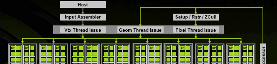
These are the delights of unification. The road to completely unified streaming processor is already open, so this issue can be considered nearly solved. But more on that later. ;-) And now let's take a closer look at... Shader processor and its TMU/ALU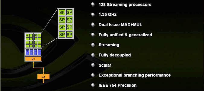
So, each of 8 shader units features 16 scalar ALUs. This, again, provides us with potential to increase efficiency of their load up to 100% independently on shader code. ALUs operate at doubled clock rate and therefore correspond to or surpass (depending on shader operations) 8 older quad-component vector ALUs (of G70) at the same base core clock rate. NVIDIA cites the following peak performance calculation: 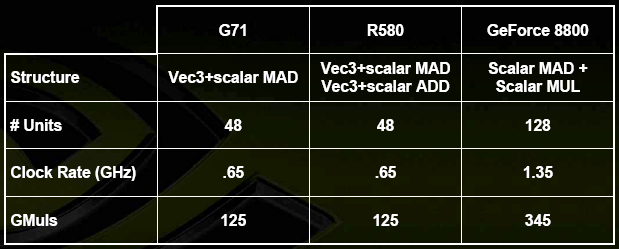
But it's actual for the double multiplication variant that is most unfavourable for others. To adapt this to real life, you should divide this advantage by 1.5 or so. But anyway these scalar ALUs are capable of outperforming all previous chips due to higher clock rate and their number. Except for maybe G7X in SLI configuration in case of shaders not very beneficial for the new architecture. We'll check this assumption further in synthetic and gaming benchmarks. It's interesting that all ALUs operate with FP32 precision, so, considering the new architecture, we can't see any benefits for FP16 shaders with reduced precision. We can finally forget this compromise (like in case with ATI's latest chips). Another interesting peculiarity is the support of integer calculations (required for SM4.) This arithmetic meets the IEE 754 standard, which makes it suitable for more serious non-game computing, including scientific, statistical or economic. But, again, more on that later. ;-) Now let's take a look at how texture units and ALUs interact within a shader unit: 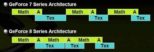
Texture prefetch and filtering operation doesn't require ALU resources and can be executed in complete parallel to math calculations. But texture coordinate generation (A on the chart) still needs some of ALU time. Well, it's logical as well, if we are going to utilize chip transistors at 100%. Texture coordinate generation requires standard FP operations and it wouldn't be prudent to implement dedicated ALUs for it. Texture units are organized in the following manner: 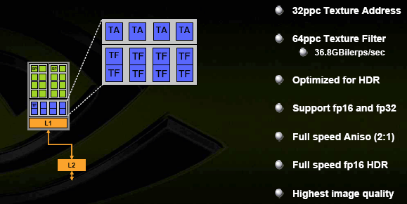
There are 4 texture addressing (TA) units that determine exact prefetch address based on coordinates, and 8 bilinear texture filtering (TF) units. Why is that so? This, at moderate transistor expenditure, makes possible free honest trilinear filtering or halves performance drop caused by anisotropic filtering. Both are typical for today's accelerator workflow, when anisotropy becomes the filtering of choice among gamers that purchase high-end cards. Performance in usual resolutions, with usual filtering and without AA, is naturally "obsolete", since the previous generation of accelerators perfectly handles even the latest games on the largest monitors under these conditions. Today's chips are AF+AA+HDR by right. About HDR by the way - it also supports FP16/FP32 texture formats. As well as SRGB gamma correction on input (TMU) and output (ROP). The vendor also promises a significant increase in QUALITY of anisotropy, saying that now it corresponds or even surpasses ATI's latest products in high-quality AF modes. Running ahead, we can say that we have checked this declaration and found it to be true! NVIDIA has actually eliminated another weak spot of its chips, so now we have excellent-quality anisotropy with only a slight performance drop (see benchmarking results further). Finally, here are the specifications of new shader model that meets the requirements of SM4: 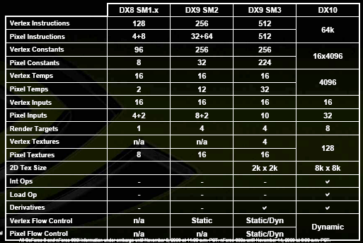
Here we have significant quantitative and qualitative changes. Fewer shader limitations and more resemblance to CPUs. For now it goes without much random access (SM4 introduces this feature (see the "Load Op" on the chart), but its general efficiency is still dubious, especially in first implementations). But there's no doubt that in the near future this will evolve like FP formats did during these 5 years - from the first tries in NV30 to a complete all-purpose FP32 pipeline in G80. ROPs, frame buffer writes, AAAs you remember, besides 8 shader units, there are 6 ROPs: 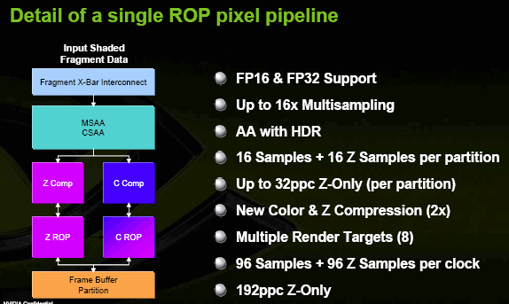
On the chart there are two separate paths for Z and C, but actually it's a single set of ALUs divided into two groups for coloured pixel processing or united for Z-Only calculations thus doubling the throughput. Today there's not need in counting pixels, since they are aplenty. More important is to count MSAA samples per clock, and this is provided. So, at MSAA 16x the chip can output 6 complete pixels per clock, at 8x - 12 pixels, etc. It's interesting that frame buffer scalability is rather good - as we remember, each ROP works with own memory controller and doesn't interfere with any other. Finally, there's complete support for FP32/FP16 frame buffer formats TOGETHER with AA. This will allow developers to fulfill their dreams, as HDR won't require any changes in general order along the pipeline even in the AA mode, since all shaders will actually remain the same, and only the data format will have to be changed. CSAAWelcome the new AA method - CSAA. While a more detailed examination will be carried out in a dedicated article scheduled to release soon, for now we'll state that it strongly resembles ATI's approach and also deals with pseudo-stochastic patterns and spreading samples to neighbouring geometrical zones (pixels are dithered, do not have sharp borders, and transform into each other thus covering a certain zone). At that sample colours and Z are stored separately from information on their location, so a single pixel might require 16 samples, but only 8 calculated Z values, which also saves bandwidth and clocks. As you know, classic MSAA becomes very memory-consuming in modes better than 4x, introducing less quality increases each step. The new method corrects this behaviour, enabling quality of AA 16x to noticeably surpass that of MSAA 16x at resource expenditure comparable to MSAA 4x. For now we'll sum up that NVIDIA eliminated weak spots here as well comparing to ATI. NVIOAnother innovation is interfaces moved outside the primary chip. Now they are located on a dedicated chip named NVIO:  It features:
Output subsystem looks like this: 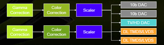
Precision is 10 bits per component on all its stages. Of course, this chip might be removed from middle-end and naturally low-end solutions, but it still offers more advantages than disadvantages for expensive cards. Interfaces occupy much chip space, are strongly affected by noise, and require dedicated power supply. Having moved them to an external chip, NVIDIA increased output signal quality and configuration flexibility, and relieved developers from consideration of RAMDAC optimal modes. Pipeline from the angle of DirectX 10 APIFirst, let's revise key features of DX10 that will become available when it's released together with the new OS: 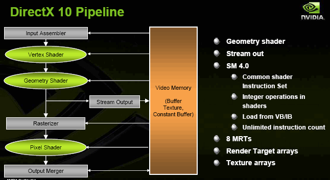

Innovations include SM4, texture and frame buffer arrays, geometry generation in geometry shaders (new shader type) and writing intermediate geometry data back to frame buffer. In total they enable completely hardware realization of previously unavailable algorithms, including smooth surfaces with recursive fragmentation, complex systems of particles interacting with each other and environment, etc. Everything here nicely corresponds to forecasts made in the article "DX.Next: The near and nearest future of hardware graphic acceleration." There are also means of reducing costs of API calls and resource virtualization. But we'll be able to estimate their efficiency in real applications only after Vista is released along the first games for it. It's important that you understand that architecture might differ from the angles of API and its hardware realization. So, here, despite this rather strict scheme, the chip itself can deal with other shader types as well. It just depends on how they are represented in API. For example, nothing prevents geometry shader from preceeding vertex shaders, etc. G80 as your personal supercomputerAnd now the dessert. The most interesting. Peak performance of G80's FP math surpasses that of any existing desktop processor. Calculations are made according to the IEE 754 standard. Unified shader architecture has enough flexibility to process not only game physics, but also math and physical modelling, economic and statistical computing. Image recognition, processing, scientific graphics... There's a vast range of tasks solvable with a good streaming processor supporting dynamic branching. What does it require? Support by applications. And what is needed for such support? A convenient calculation-oriented API that will outlive one or two accelerator generations and will be suitable enough for fast adaptation and development of applications offloading calculations to GPU. Trumpets ready... Now, with the release of G80, we have such an API for NVIDIA chips! 
CUDA (Compute Unified Device Architecture) - an architecture designed for various tasks and realized as a special SDK, API and Ñ compiler, as well as small hardware implementations into G80 (some special computing mode, in which data is processed by dispatcher <-> shader unit <-> cache without separation to pixels, vertices, etc.) that, to all appearances, doesn't require any significant architectural changes, just some data "bypass routes". Now they can develop applications that will use suitable hardware acceleration in the form of G80 and its successors for various intensive streaming and vector calculations. In the future we'll try to review this in a separate article and measure the real performance in typical tasks. For now, we can state that NVIDIA has declared the boost ranging from ten-time (!) to several-hundred-time depending on task comparing to a dual-core Core 2 Duo 2.66 GHz. The key benefit of such solution is its independence of DX and hardware. Programmers will only have to work according to SDK, not going into details of realization and compiling. They won't have to study shader model and write separate shaders for their computing tasks. And that means this solution might become a de facto standard. And good bye to any 3rd party physics accelerators. ;-) General trendsAlready now it's obvious that the struggle between processor and graphics leaders has begun. AMD purchased ATI to pose as a united force on the field of future unified graphics-computing processors. While NVIDIA seemingly feels itself all right alone, pumping muscles in the chipset market, where its share grows with every novelty, and looking at CPUs, complexity of which doesn't scare the company anymore (and it also has licenses from Intel and AMD for generally accepted buses.) Of course, they won't be releasing desktop processors in the nearest year or two to compete with the titans, but, perhaps, in the near future we will see some exotic attempts somewhere on the edge of mobile processor market. There's no doubt that in 5-10 years graphics accelerators, following the path of increasing universality and flexibility, and central processors, following the path of parallelism, will eventually converge. A single chip will contain a set of probably heterogeneous cores, both computational, graphic, and general-purpose. Also onboard will be everything that yesterday was called "Northbridges" (we can already witness this in some AMD's server architectures) - memory controllers, processor and general-purpose buses. This great convergence might also become the great revision of the Wintel market, in which both new players like NVIDIA and new OSes might get their chances. Of course, some might want to follow an easier path and get under the wing of a large processor/platform company like ATI has done. Yes it will be easier, but victories are not gained by easiness. NVIDIA is on the great rise now and it feels strong enough to become (at least) another industry "engine", a role that has been performed for so many years by Intel that recently has been slightly out of breath. Well, as you might have already guessed, only the time will tell. ;-) Hi-Tech is the most appropriate for this saying. And now let's proceed to benchmarking results! NVIDIA GeForce 8800 GTX (G80) - Part 2: Graphics Card Features And Synthetic Benchmarking ResultsWrite a comment below. No registration needed!
|
Platform · Video · Multimedia · Mobile · Other || About us & Privacy policy · Twitter · Facebook Copyright © Byrds Research & Publishing, Ltd., 1997–2011. All rights reserved. |


