NVIDIA GeForce GTX 580 Graphics Card
|
Design
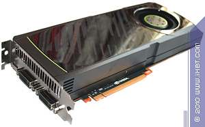
| NVIDIA GeForce GTX 580 1536MB |
- GPU: GeForce GTX 580 (GF110)
- Interface: PCIe x16
- GPU clock rate (ROPs/Shaders): 775/1550 MHz (standard)
- Memory clock rate, physical (effective): 1000 (4000) ÌÃö (standard)
- Bus width: 384-bit
- Stream processors: 512
- TMUs: 64 (BLF/TLF/ANIS)
- ROPs: 48
- Size: 270x110x39mm
- PCB color: black
- RAMDACs/TDMS: integrated into GPU
- Outputs: 2 x DVI (Dual-Link/HDMI), HDMI mini
- Multi-GPU: SLI (Hardware)
|

|
| NVIDIA GeForce GTX 580 1536MB |
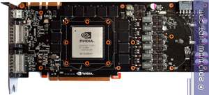
| 1536MB of GDDR5 SDRAM in 12 Hynix chips on the front side of the PCB. |
 |
| Comparison with the reference design, front view |
| NVIDIA GeForce GTX 580 1536MB |
Reference NVIDIA GeForce GTX 480 |

|

|
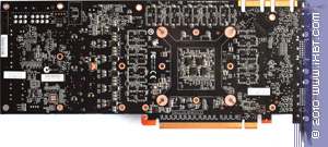
| Comparison with the reference design, rear view |
| NVIDIA GeForce GTX 580 1536MB |
Reference NVIDIA GeForce GTX 480 |

|

|
As you can see, the design hasn't changed much. GTX 580 just has no ventilation hole. Other changes are minor, but that's only logical since the GF110 GPU is similar to GF100. The card has a standard size for a high-end solution, so it should fit into any enclosure.
The novelty has supplementary power connectors: one 6-pin and one 8-pin, so make sure you have an adapter.
Maximum resolutions and frequencies:
- 240 Hz maximum refresh rate
- 2048 x 1536 x 32bit @ 85Hz Max -- analog interface
- 2560 x 1600 @ 60Hz Max -- digital interface (Dual-Link DVI/HDMI)
As for the HDTV support, a review is available here.
According to the image, the chip was made on the 38th week, i.e. in September.
Write a comment below. No registration needed!
|
|
 |
|
|
|
