 |
||
|
||
| ||
|
||
|
||
| ||
We had been waiting for this moment for a year, maybe even two. But manufacturing troubles and other issues kept delaying the rollout of NVIDIA's Fermi-based solution. Finally, the novelty has been announced, and we're going to examine it in detail. It was high time NVIDIA updated its graphics architecture, because company's previous GPUs only supported DirectX 10 and DirectX 10.1, while the primary competitor had been offering DirectX 11 solutions since fall. Besides, the number of games utilizing this API have been evergrowing. Though the first information about the new architecture came to light not very long ago, it seems like the wait was too long nevertheless. Well, the Fermi architecture was announced the last autumn, and almost all technical details were revealed in January. That's why it seems we've had to wait for about six months, while the rollout has only been delayed for a quarter. Initially they planned to release the novelties in Q4'09. Anyway, the reason for the delay is kinda simple and is not just NVIDIA's fault. Naturally, it was only possible to manufacture such a big and powerful GPU -- with more than 3 billion transistors on board -- using the new 40nm process technology of TSMC. That where trouble started. The long and painful mastering of the process technology started with AMD mobile GPUs and the desktop RV740 (which wasn't very successful), as well as NVIDIA's GT21x mobile graphics. The competitor managed to master the technology a bit faster, since its top-end solution RV870 was considerably simpler in terms of the amount of transistors, and also because that was an upgrade of the old architecture, not the completely new one, like GF100. Then other GPUs, aimed at mid-end and low-end price ranges, were released, but the manufacturing trouble remained. AMD still doesn't have enough 40nm GPUs to satisfy the market. Obviously, such unpolished and problematic manufacture couldn't help release the complex GF100 any faster. Mind you, it was hard to roll the GPU out at all, in its initial form. A lot depended on actual clock rates and other specifications of real graphics cards. Today we shall see how that will turn out. But firstly you may want to read the previous reviews to get a better idea of what the GeForce GTX 200 (GT200) architecture is. Essentially, its the further development of the G8x/G9x architecture, featuring certain changes. Here you go: All right, now let's delve into the details of the new graphics processing unit and two new GeForce GTX 400 series graphics cards. GeForce GTX 400 series specifications
GeForce GTX 480 reference card specifications
GeForce GTX 470 reference card specifications
The 40nm process technology allowed NVIDIA to make a powerful GPU featuring 3 billion transistors. This is the company's most complex GPU of all time. It does have a lot of new features we'll describe further. For now let's talk about product naming. The naming policy remained the same. The first number changed compared with the previous top-end cards. Note that it changed from 2 to 4, bypassing 3. It was done, because there was already a 3 series based on older GPUs and aimed at OEM builders. The new GTX 470 and GTX 480 should seemingly replace GTX 275 and GTX 285, at a lower price, and there will probably be no cards like GTX 295. While there's trouble with making GF100 chips according to the new process technology, many previous-generation cards will be produced and sold at lower prices. As it usually is with NVIDIA graphics cards, the two models have different clock rates and the number of disabled processors. GTX 480 has 480 streaming processors, 60 TMUs and 48 ROPs, while GTX 470 has 448 stream processors, 56 TMUs and 40 ROPs. As you can see, there are no full-fledged models so far. Both products are reduced one way or another. The performance difference between the two should be about 20-25%. Chips incapable of working at 700/1401 MHz with 480 stream processors enabled will be used to make GTX 470. Both models feature GDDR5 memory to eliminate bottlenecks, but have different VRAM capacity and bus widths. The higher-end product utilizes full-fledged 384-bit memory bus, while the lower-end model has one of 64-bit controllers disabled, and it only has 320-bit bus. This, in turn, affects memory capacity. The 384-bus allows installing 768MB, 1536MB or 3GB of VRAM, while the 320-bit one allows installing 640MB, 1280MB or 2560MB of memory. Obviously, NVIDIA chose 1536MB and 1280MB, because 640MB/768MB is not enough and 3GB has no sense. Actually, these capacities are quite beneficial. Even if, on a rarest occasion, an application runs out of 1GB of memory, there will be another half to use. The two solutions also have different PCB layouts and coolers. The GTX 470 has a simpler cooling system, but it's still dual-slot. As for power consumption, it differs as well, but not very much: 215W vs. 250W. GF100 key featuresOf the "GF100" codename "GF" stands for "Graphics" and "Fermi," while "100" means the first GPU of the architecture aimed at the high-end price range. The GF100 architecture supports all the features of the DirectX 11 API, including hardware tessellation and DirectCompute. Moreover, it has leeway for the future features of the API, as well as the needs of graphics applications, like ray tracing and physical effects. Comparing to the previous architecture, GF100 utilizes the 3rd generation of Streaming Multiprocessors with more than twice the number of CUDA cores. The number of other execution units has also grown. But the key change is that the geometry pipeline has been considerably reworked. To meet the requirements of DirectX 11 and modern graphics applications, the new GPU offers a considerably higher peak performance of geometry processing, geometry shaders, and stream out. What's also important, the new GPU is very fast in terms of tessellation, DirectX 11's key innovation. In the new GPU, the traditional geometry processing architecture is replaced by a new architecture utilizing several PolyMorph Engines and Raster Engines, which work in parallel -- compared with single units in all the previous GPU generations. The new memory subsystem architecture is another plus. Full-fledged L1 and L2 caches provide fast access to geometry data for stream processors and tessellation units. GF100 has other advantages as well, which uncover the capabilities of the Fermi architecture. Recently, general-purpose computing has seen much attention. These have special requirements to hardware. So, the key changes of GF100 related to improving the efficiency of computing algorithms, including quick context switching between graphical and general-purpose computing, competitive execution of computing programs and improved caching architecture, effective for tasks like ray tracing and artificial intelligence. Other innovations include improved performance of atomic operations, which speeds up algorithms like order independent transparency rendering. GF100 architectureLike the previous NVIDIA GPUs, GF100 consists of several clusters, which are now called Graphics Processing Clusters. Each of those consists of several Streaming Multiprocessors (SM), which, in turn, contain arrays of stream processors. 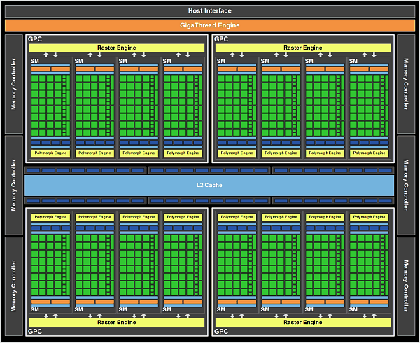 GF100 features 4 GPC, 16 SM and six 64-bit memory controllers. NVIDIA has released two graphics cards on GF100 so far -- GTX 470 and GTX 480 -- with the different number of GPC clusters and memory controllers. This is logical from the production angle, because TSMC's process technology doesn't allow making large quantities of full-fledged GPUs. Such an approach also meets company's marketing policy of offering different products for different price ranges. So, the new GPU features a PCI Express interface, a GigaThread engine, 4 GPC, 6 memory controllers, 6 ROPs, and 768KB of L2 cache attached to ROPs. GPU gets instructions via the Host Interface, the GigaThread engine requests needed data from system memory and copies it to local memory. Unlike the previous GPU that had eight 64-bit memory controllers, GF100 only has 6, but supports GDDR5 memory, one thing GT200 couldn't provide. GDDR5 memory and 384-bit access result in quite a high bandwidth. The GigaThread dispatcher is the center of the GPU, it creates and allocates streams to Streaming Multiprocessors. SM allocate warps (groups of 32 streams) to CUDA cores and other execution units. GF100 features 512 stream processors organized into 16 Multiprocessors. The actual graphics cards have a fewer number of those: 448 (14 SM) in GTX 470 and 480 (15 SM) in GTX 480. Each SM can process up to 48 warps simultaneously, while one CUDA core can execute all program types, including vertex, pixel, geometrical, computing. GF100 features 48 ROPs which handle pixel blending and antialiasing, as well as atomic memory operations. ROPs are organized into 6 groups, each has its own 64-bit memory controller. As you already know, GTX 470 has one ROP disabled, so it has a 320-bit bus and 40 ROPs. Write a comment below. No registration needed!
|
Platform · Video · Multimedia · Mobile · Other || About us & Privacy policy · Twitter · Facebook Copyright © Byrds Research & Publishing, Ltd., 1997–2011. All rights reserved. |


