 |
||
|
||
| ||
|
||
|
||
| ||
Part 1. Theory and architecture
 Several months have passed since the release of the top series of DX10 accelerators GeForce 8800, it will be half a year soon. Mid-end video cards usually come in 3-4 months, but not in half a year. Perhaps, the upgrade to the 0.08 micron process technology was not that easy. There might have been other reasons, probably marketing ones. The notorious problems with the quality of drivers for 8800 cards might have emerged, and NVIDIA might have decided to delay the launch until the most troublesome problems are fixed. It's no secret that many forums are still buzzing as hives about how GeForce 8800 supports various games. Not only in Vista, but in good old Windows XP as well. The quality of drivers is starting to improve now. Probably Mid-End solutions were timed to this. But these are only our guesses and assumptions. The fact is, GeForce 8600 (G84) and GeForce 8500 (G86) have been launched. Look at the collage on top. You will see that the 8600 is a quarter of the 8800. We do not mean dimensions, of course :-) Otherwise, the 8600 GTS would have been just 7 cm long. :-) We speak of technologies and GPU capacities. Have a look: the 8800 has 128 stream processors, while this card has only 32. 32 versus 16 texture units (tests show only 8 of them). Bus: 384 bit in the 8800 versus 128 bit in the 8600. And so forth. Why cut G80 down so much? It deals a strong blow to performance! And the gap between the lower Hi-End 8800 GTS 320MB and the upper Middle-End 8600 GTS will be very large in terms of performance and much smaller in terms of prices. But we should still check it up. One thing is clear: such cards have a great potential for dropping prices, because their cores and PCBs are very cheap. Another thing is certain: reference cards will rule again. The practice of manufacturing all video cards at a single plant and then selling them to partners is passing from Hi-End to Middle-End.
And now Alexei Berillo will tell us about all innovations of this architecture: Mid-End solutions from NVIDIA have finally upgraded to the long-awaited unified graphical architecture. This upgrade was initially done in the High-End solution — GeForce 8800. But not all people could try the new architecture, most of them were waiting for Mid-End and budget solutions based on such architectures. Today we are going to examine the first inexpensive solutions from NVIDIA based on the unified G8x architecture: Before you read this article, you had better look through the fundamental materials on DX Current, DX Next and Longhorn that describe various aspects of modern hardware video accelerators and architectural peculiarities of products from NVIDIA and ATI(AMD).
These articles predicted the current situation with GPU architectures, a lot of forecasts on future solutions came true. Detailed information on the unified architecture of NVIDIA G8x (by the example of the top GPU) can be found in the following article:
Much time passed since the announcement of NVIDIA GeForce 8800, but ATI(AMD) still hasn't responded with its own unified architecture. So when their announcement is round the corner, NVIDIA decides to make another strong marketing move and launch two new chips and several Mid- and Low-End models. The main technological change is 80 nm process technology (0.08 micron). It allows to reduce the cost of products, which is especially important for inexpensive cards. All new chips are cut-down modifications of G80. They are intended to press their competitors in Low- and Mid-End price segments. The architecture of new chips is based on GeForce 8800 (G80). G84 and G86 chips include all advantages of G80, such as unified shader architecture, full support for DirectX 10, high-quality methods of anisotropic filtering and a new algorithm of CSAA with up to 16 samples. Now all these features are available in Low- and Mid-End segments ($89-$229). Moreover, some units have been improved since G80. GeForce 8600
The first G84-based video cardsReference GeForce 8600 GTS Specifications
Specifications of the reference card GeForce 8600 GT
GeForce 8500
Specifications of the reference card GeForce 8500 GT
As you can see, GeForce 8600 exists in two modifications — GTS and GT. The former operates at 675 MHz and 1450 MHz (core and shader processors). Frequencies of the latter are 540 MHz 1190 MHz. Video memory clock in these modifications differs as well: 1000(2000) and 700(1400) MHz. GeForce 8600 GTS is intended to replace GeForce 6600 GT and GeForce 7600 GT, which used to be the most popular cards in this price segment. The GT model is a step lower in this series. The Low-End segment is represented by GeForce 8500 GT, which chip is cut down even to a greater degree. Perhaps, G86 will be later used to launch other models, for example, GeForce 8400 GS and GeForce 8300 GS. They may appear as OEM products and be unavailable in retail. Technical characteristics of the latter (the number of processors, ROPs/TMUs, clocks) are unknown so far. ArchitectureJudging by specifications alone, we can see that G84 is something in between one fourth and one third of G80. It's one fourth in terms of unified processors, and it's one third in terms of ROPs and the memory controller. The situation with texture units is more complex - it's not one fourth, and it's not a half. We'll dwell on it later. In its turn, G86 is something interesting — it's only 1/8 of G80 in terms of computing power, and it's still 1/3 in terms of ROPs. NVIDIA is evidently reluctant to take its fast chips down to Low-End. The main question here is whether this quarter and 1/8 are sufficient to compete with the existing solutions and future GPUs from AMD. Perhaps NVIDIA cut down too many units? In fact, both solutions aren't too small in terms of transistors... G84 contains almost half as much transistors as G80, G86 — almost one third of the quantity. It seems like a compromise. If half of G80 units had been preserved, the chip would have been too expensive to produce, and it would have competed well with GeForce 8800 GTS. To all appearances, the 65 nm technology will be used in future for faster Low-End chips. As for now, we've got only this solution. We'll analyze performance of the new chips in synthetic tests and games. But even now we can say that G84 and G86 may be quite slow because of few ALUs. Most likely, they will be on a par with the existing solutions for similar prices. We shall not analyze the architecture of G84 and G86 in detail, because there aren't many changes from G80. Everything written about GeForce 8800 applies here as well, adjusted for the present quantitative characteristics. But we'll still provide the highlights worthy of our attention and publish several slides devoted to architectural specifications of the new chips.
Here is a diagram of a video chip based on the G80 unified architecture:
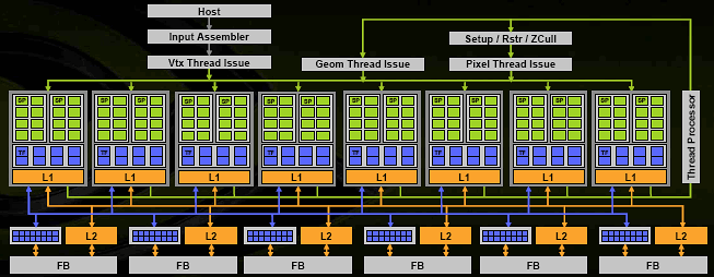 G80 consists of eight unified shader processors, NVIDIA prefers to speak of 128 processors. To all appearances, a command execution unit is a group of four TMUs and 16 ALUs. Each unit can execute a part of a vertex, pixel, or geometry shader over a block of 32 pixels, vertices, or other primitives. They can also compute physics. Each processor has its L1 Cache to store textures and other data. Along with a dispatcher and shader processors, there are six ROP partitions, which determine visibility, write values to a frame buffer and MSAA. They are grouped with memory controllers, write queues, and L2 cache. This architecture can be scaled both ways, which has been done in the new solutions. We've already mentioned this elegant solution that implements the main advantage of the unified architecture (automatic balance and efficient usage of available resources) in the review of GeForce 8800. The Mid-End solution was expected to possess half of computing units. And a solution with two shader processors and one ROP was to be a budget product. Unfortunately, while GeForce 8800 had eight processors consisting of 32 TMUs and 128 ALUs, the new chips have fewer units than had been expected. To all appearances, the G84 block diagram looks like this:  That is, everything is unchanged, except for the number of units and memory controllers. There are minor changes in texture units, which you can see in this picture. But we'll deal with them later. I wonder where all those transistors are, if G84 has only 32 processors? G84 contains almost half of transistors compared to G80, but it has much fewer memory channels, ROPs, and shader processors. G86 also has a lot of transistors and just 16 processors... It's also interesting how well the load will be balanced in real applications between vertex, pixel, and geometry shaders - as there are much fewer unified execution units now. Especially as the unified architecture itself sets new tasks to developers. When it's used, they have to think about efficient usage of the total capacity for vertex, pixel, and geometry shaders. Here is a simple example — limited by pixel processing. In this case a higher load on vertex units in the traditional architecture will not result in a performance drop. But in case of the unified architecture, it will change the balance and reduce the amount of resources allocated for pixel processing. We shall analyze the performance issue later. And now we'll proceed with the review of changes in the architectures of G84 and G86. Shader processor and TMU/ALUThe block diagram of shader units and analysis of G80's peak performance were published in the corresponding article. The block diagram for G84 and G86 hasn't changed, and it's not difficult to recalculate their performance. Scalar ALUs in these chips also operate at the doubled frequency, which makes them very efficient. There are no differences in functionality either. Precision of all ALUs is FP32. They support calculations in integer format. They are IEEE 754 compliant, which is important for scientific, statistical, economic, and other calculations.
But texture units have changed compared to those in G80. According to NVIDIA, the architecture of the new chips is modified to increase performance of unified processors. Each texture unit in G80 could compute four texture addresses and execute eight texture filtering operations per cycle. The company claims that the first number has been doubled in the new chips and that it can do twice as many texture fetches. That is, texture units in G84 and G86 have the following configuration (the block diagram of G80 is published in the left):
 According to NVIDIA, each unit now has eight texture address units (TA) and just as many texture filtering units (TF). G80 had four TA units and eight TF units, which provided "free" trilinear filtering with fewer transistors or twice as small performance drops from anisotropic filtering. This is useful for High-End video cards, where anisotropic filtering is almost always enabled. We'll check it out in the practical part. You must have a look at the analysis of corresponding synthetic tests, because they contradict these data. The other functions of texture units are identical, they support FP16/FP32 texture formats, etc. But G80 allowed FP16 texture filtering at full speed owing to the doubled number of filtering units, while Mid-End and Low-End solutions cannot do that (provided the above mentioned changes are real). ROPs, writing into a frame buffer, antialiasing
ROPs (six units in G80, two units in the new GPUs) haven't changed:
 Each unit processes four pixels (16 subpixels), totaling 8 pixels per cycle for color and Z. Twice as many samples are processed per cycle in Z only mode. In MSAA 16x mode, the GPU can process two pixels per cycle, in 4x mode — 8 pixels, etc. Like in G80, these GPUs offer sterling support for FP32 and FP16 frame buffer formats with antialiasing. Like GeForce 8800, the new GPUs support the new antialiasing mode — Coverage Sampled Antialiasing (CSAA), which was analyzed in the following article:
Here is a recap of the method. Color and Z values of samples are stored separately from their addresses. One pixel may have up to 16 samples and just eight Z values to save bandwidth and cycles. CSAA allows to do with transmitting and storing a single color value or Z value of each subpixel. It specifies more accurately the averaged value of a screen pixel by using precise information how this pixel covers triangle borders. As a result, the new method allows 16x AA, which offers much higher quality than MSAA 4x, at similar computing expenses. On rare occasions, when CSAA does not work, users just get usual MSAA of lower degree instead of no antialiasing at all. PureVideo HDLet's proceed to the most interesting changes. It turns out that G84 and G86 have innovations that give them some advantage over G80! We speak of the built-in video processor, which features enhanced support for PureVideo HD. They are said to fully offload the CPU of all video decoding tasks, including the "heaviest" H.264 format. G84 and G86 use a new model of programmable PureVideo HD video processor. It's more powerful than the one used in G80, and it includes the so-called BSP engine. The new processor can decode H.264, VC-1 and MPEG-2 formats of up to 1920×1080 with the bitrate up to 30-40 Mbps. It does all the work to decode CABAC and CAVLC data on the hardware level, so it can play all existing HD-DVD and Blu-ray discs even on Mid-End single-core computers.
The video processor in G84/G86 consists of several parts: Video Processor of the second generation (VP2) responsible for IDCT, motion compensation, and artifact removal for MPEG2, VC-1 and H.264 formats, it can decode the second stream on the hardware level; Bitstream processor (BSP) responsible for statistic CABAC and CAVLC decode for the H.264 format, as these are the most intensive computations; AES128 engine — it decodes video data protected from copying in Blu-ray and HD-DVD. Have a look at the differences in hardware support for video decode in various GPUs: 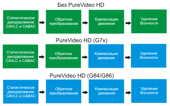 Blue tasks are executed by a GPU, green tasks are executed by a CPU. As you can see, the previous solution helps a CPU only in some tasks, but the new GPU does everything on its own. We'll analyze the efficiency of these solutions in future articles devoted to video decoding on the hardware level. NVIDIA publishes the following numbers: Software decode of Blu-ray or HD-DVD gobbles up to 90-100% time of a modern dual-core CPU. Hardware decode takes up 60-70%, of a prev-gen CPU on the same computer. But the new engine in G84 and G86 uses just 20%. It does not look like fully hardware decode, but it's still very efficient. The new features of PureVideo HD currently work only in Windows Vista 32bit, and Windows XP will get PureVideo HD only in summer. What concerns the quality of video playback, post processing, deinterlacing, etc, NVIDIA had improved it in GeForce 8800, and the new chips are no different in this respect. CUDA, non-gaming and physics computingThe article about GeForce 8800 mentioned that the increased peak performance of floating point arithmetic in new video cards and flexibility of the unified shader architecture are sufficient to compute physics in games and even more serious tasks: mathematical and physical modeling, economic and statistical models and computations, OCR, image processing, scientific graphics, and so forth. A special API intended for computations was developed for this purpose. It's convenient for adaptation and development of programs that offload computations to the GPU — CUDA (Compute Unified Device Architecture).
CUDA is reviewed in detail in the article about G80. We are going to dwell on another modern trend — GPU support for computing physics. NVIDIA calls this technology Quantum Effects. The company declares that all video chips of the new generation, including G84 and G86, cope well with such computations. They allow to shift some load from CPU to GPU. Examples include smoke, fire, explosions, hair and cloth dynamics, fur and fluids, and so forth. But we'd like to write about the real thing. We are shown only pictures from test applications with a lot of physical objects computed by GPUs. Games with this support are nowhere to be found so far.
 Support for external interfacesAs you may remember, we were surprised by some new feature in GeForce 8800 — an additional chip that supports external interfaces. In case of top video cards, a separate chip called NVIO is responsible for these tasks. It integrates two 400 MHz RAMDACs, two Dual Link DVIs (or LVDS), HDTV-Out. We suspected at the time that Low- and Mid-End products would hardly retain a separate chip. We were right. Support for all interfaces is built into the GPU itself in G84 and G86. GeForce 8600 GTS is equipped with two Dual Link DVI-I outputs with DHCP support. It's the first video card in the market with such features (HDCP and Dual Link together). What concerns HDMI, this connector is fully supported on the hardware level. It can be implemented by manufacturers on cards of special design. But support for HDCP and HDMI is optional in GeForce 8600 GT/8500 GT. But they can still be added by some manufacturers to their products. And now we proceed to the practical part of our article. We'll find out whether the significant reduction in execution units of the new GPUs had a serious effect on their performance. They will be compared to competing products and prev-gen solutions from the same manufacturer. NVIDIA GeForce 8600 GTS (G84). Part 2: Video cards' features and synthetic testsWrite a comment below. No registration needed!
|
Platform · Video · Multimedia · Mobile · Other || About us & Privacy policy · Twitter · Facebook Copyright © Byrds Research & Publishing, Ltd., 1997–2011. All rights reserved. |


