 |
||
|
||
| ||
|
||
|
||
| ||
Part 1. Theory and architecture
 Contents
We all know that the first video cards supporting DirectX 10 appeared in the end of 2006. They were top products from NVIDIA (GeForce 8800 GTX is still the fastest card (it even has an overclocked modification - 8800 Ultra)). The Californian company has already launched Mid-End video cards with DX10 support, and the competitor was still silent. ATI has offered no top products for almost a year and a half already. We understand all difficulties that have to do with the merger with AMD. Organizational and personnel matters required some time to settle, which slowed the R600 development down . By the time everything was ready, some people in AMD decided to time the launch of the top product to the launch of the entire series of Mid-End video cards. Hence the delay with the announcement. And finally the announcement has been made! But the Canadians (or are they Americans now?) have problems again - now with Mid-End cards. Today we'll publish only their general description and theory. But we'll be able to learn about the real capacities of these products only in July. We don't want to sound sad, but the past events indicate that the ATI/AMD's business of video cards is slowly fading. Market analysis reports periodically published by competent companies also prove it. AMD has bought ATI with a distant goal - to focus on integrated solutions - the future is theirs. Hence the problems with the launch of DX10 family from ATI... Besides, there is no top product to compete with the fastest accelerator from NVIDIA. HD 2900 XT (R600) can compete only with GeForce 8800 GTS, and it will have a matching price. We should add that there are almost no games for DX10, so we cannot know the layout of forces in the new games. So, it's too early to draw conclusions. Perhaps, the new series from ATI will please many users (including product prices), and the delay of the AMD's Canadian department will not be fatal.
And now Alexei Berillo will tell us about all innovations of this architecture: In our recent review of G84 and G86 we complained that NVIDIA had launched High-End solutions long ago, other GPUs based on the unified G8x architecture followed in spring, but similar DirectX 10 solutions from AMD were not even announced yet. And now the long-awaited moment has come - today AMD is going to announce almost an entire series. "Almost" - because the series lacks the fastest solution to compete in the High-End segment. The stress is on the word "announce" - because Mid- and Low-End video cards on the new chips will be available a tad later. Today we are going to publish only theoretical information. The main difference between RV630/RV610 and the top R600 is the 65 nm process technology. It allows to reduce production costs, which is important for inexpensive products. It probably affected the release dates of these products. Before you read this article, we traditionally recommend that you should look through the fundamental materials on DX Current, DX Next and Longhorn that describe various aspects of modern hardware video accelerators and architectural peculiarities of products from NVIDIA and ATI(AMD). These articles predicted the current situation with GPU architectures, a lot of forecasts on future solutions came true.
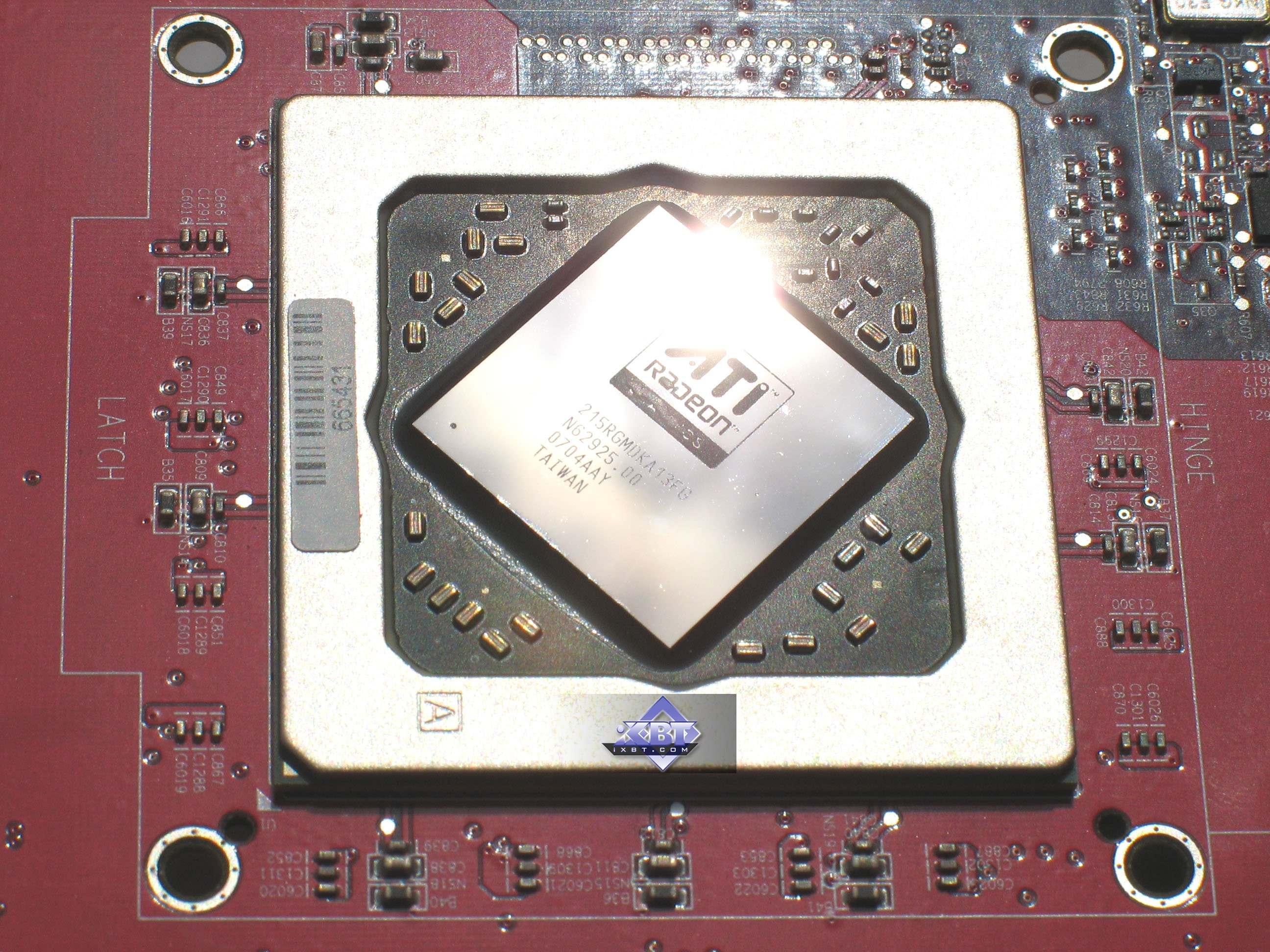
For AMD(ATI) it's the second generation of the unified architecture, if we take into account not only PC solutions. The first ATI's video chip of that kind was developed for Microsoft Xbox 360. All new solutions for personal computers are functionally identical, unlike NVIDIA products. All AMD chips from this series feature the same 3D and video decode functions. So, today we are going to meet the first DirectX 10 GPUs from AMD based on the unified architecture R6xx. RADEON HD 2900 XT
Specifications of the reference card RADEON HD 2900 XT
RADEON HD 2600 PRO and HD 2600 XT
RADEON HD 2600 XT Specifications
RADEON HD 2600 PRO Specifications
RADEON HD 2400 PRO and HD 2400 XT
RADEON HD 2400 XT Specifications
RADEON HD 2400 PRO Specifications
The key features of the top R600 solution: About 700 million transistors, 512-bit memory bus, 320 stream processors, programmable hardware accelerator, improved support for video decoding - Avivo HD, native CrossFire support. The new GPUs feature a unified architecture. All of them possess full support for DirectX 10 and even more - some features that will appear only in the next versions of this API. Judging by announcement dates, AMD must be the first to enter the market with Mid- and Low-End solutions, their chips are manufactured by the 65 nm process technology. It's important for many reasons. The 65 nm process technology provides several advantages. It allows higher density (small core size or more transistors on the same surface area). It must increase the frequency potential of GPUs and the yield of chips that can operate at high clocks, as well as reduce manufacturing costs in the nearest future. And finally, the new mid-end and low-end chips from AMD will consume much less power and thus release less heat. It will make them more attractive to potential users, and affect manufacturing costs. Architecture
The R6xx architecture combines several solutions from the previous architectures: R5xx and Xenos (a video chip from Microsoft Xbox 360), and adds some innovations: a more powerful dispatch processor, superscalar architecture of shader processors with dedicated branching units, an updated 512-bit ring bus. Here is the architecture of the top R600 GPU:
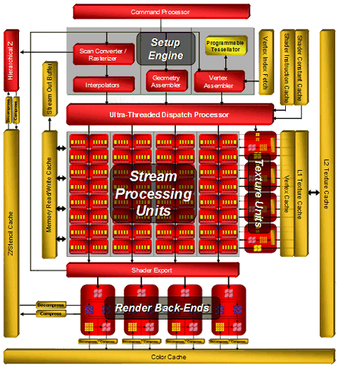 The block diagram shows that the main computing power lies in 64 superscalar stream processors, each containing 5 ALUs and a dedicated branching unit. AMD prefers to specify their number in total - 320 stream processors. We all know that manufacturers love to publish big figures. So according to the manufacturer, peak performance of a single R600 is 475 GigaFLOPS. This result can hardly be obtained in real algorithms.
Ultra-Threaded Dispatch Processor controls execution of threads by execution units. It decides which task will be executed by this or that unit depending on requirements and priorities. The new Ultra-Threaded Dispatch Processor in R6xx can service thousands of threads simultaneously, here is its block diagram: 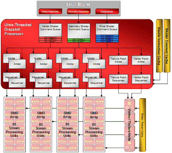 Among other changes we can mention the Command Processor, which processes commands of the video driver. It executes a micro code, thus offloading the CPU and increasing performance in case of many draw calls with little geometry to process (the small batch problem in Direct3D). It's said that the effect from the command processor appears in Direct3D 9 and Direct3D 10 applications. Theoretically, reducing CPU overheads can win up to 30%, but real results will be much lower, of course.
The new architecture seems to scale well both ways. We can see it by the example of low-end and mid-end solutions. Block diagrams of RV630 and RV610 chips:
  RV630 differs from R600 only in the number of various units: ALU, ROP, TMU. In other respects it's a copy of its senior brother. RV610 has more differences, not only quantitative ones (there are even fewer ALUs and TMUs), but qualitative ones as well: there is no hierarchical Z buffer, no texture cache of the second level, its only level caches both vertex and pixel data. The main quantitative changes: the number of shader processors has been reduced to 24 (120 processors) in RV630 and 8 (40 processors) in RV610; texturing units were reduced to 8 and 4 correspondingly; and low-end chips have four ROPs. This is done because of fewer transistors, and it will certainly affect performance. We'll analyze this issue in the future article devoted to new Mid- and Low-End solutions from AMD. I wonder how well real applications will balance the load between vertex, pixel, and geometry shaders - in case of the unified architecture developers should take care of efficient distribution of the total capacity of stream processors between various shader types. For example, when performance is limited by pixel computations, increasing the load on vertex units in the traditional architecture does not result in a performance drop. But in case of the unified architecture, it will change the balance and reduce the amount of resources available to pixel computations. Shader processors (ALU)ATI designed a non-typical solution (different from NVIDIA designs) even in the previous generation of GPUs - R580 was equipped with 48 shader units and 16 texturing units, while G70 had 24 TMUs and pixel processors and 16 ROPs. In fact, this difference in approaches has become evident even in RV530 and RV560, which had the same proportions of TMUs and shader processors. NVIDIA traditionally pays a tad more attention to texturing and fillrate, while AMD(ATI) cares for operations over pixels and vertices.
While, shader processors in previous solutions from ATI contained vector and scalar units (they could execute two instructions per cycle over 3+1 or 4+1 components), now each of 64 processors can execute 5 instructions over 5 components. Each stream processor consists of five independent scalar ALUs. They can execute five MAD (Multiply-Add) instructions per cycle. And one of five ALUs can perform a more complex instruction: SIN, COS, LOG, EXP, etc. GPU also contains a branching unit that frees main ALUs from these tasks and levels losses from jumps in a branching shader code. 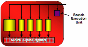 R6xx ALUs have standard functions for DirectX 10 solutions. FP32 for all computations, support for new integer formats. They are IEEE 754 compliant, which is important for scientific, statistical, economic, and other computations. The number of such execution units in R600 is very big. But when we compare it with the competing solution from NVIDIA, we should take into account the doubled frequency of shader processors in the latter. Scalar and superscalar architectures should also be compared with caution, both of them have pros and cons. For example, each unit in the superscalar architecture can process several independent instructions simultaneously (up to five math instructions and one branching instruction in this case) per pass. But this architecture has a weak spot - an application and a driver must constantly generate as many independent instructions as possible so that execution units are not idle (to preserve high efficiency). The scalar architecture does not have this limitation. It's more flexible, and it will always be more efficient, because 3D applications use different command combinations. Many of them depend on previous commands, and it's not that easy to issue 4-5 independent commands. A high-quality optimizing recompiler of shaders and optimizations in applications is required to increase efficiency of the superscalar architecture. The striking example in this case is the superscalar architecture NV3x, which benefits much from the recompiler and optimizations. Of course, the R6xx does not have evident bottlenecks like NV3x. But the architecture still benefits from optimizations. In fact, it's wrong to compare so different modern architectures only by the number of execution units. We should analyze solely results of synthetic and game tests. Besides, we must understand precisely what they mean and what units act as bottlenecks in each test. And all these great numbers are more important for marketing rather than for determining the real performance level. Texture units (TMU)
The R6xx architecture uses new texture units (to be more exact, texture and vertex sampling units in the unified chips). They are separated from stream processors, so that the system can start sampling data before they are requested by a shader unit (everything is controlled by the Ultra-Threaded Dispatch Processor, so it can give a pre-emptive task), which can theoretically increase performance. Texture units of the R6xx GPU (by the example of top R600) have the following configuration:
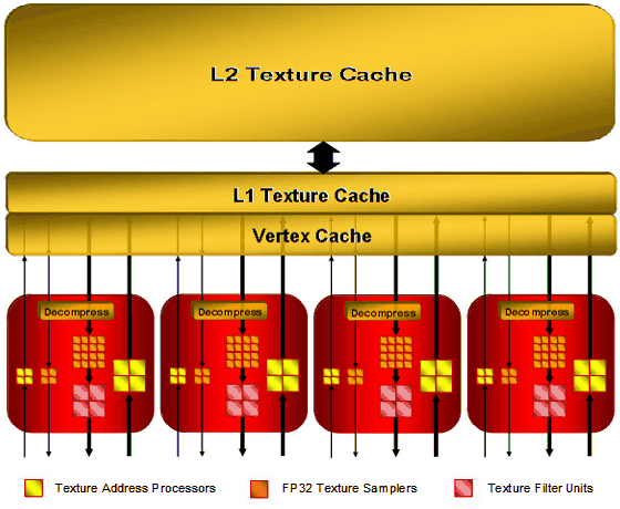 There are four texture units all in all. Each of these units consists of: 8 texture address processors (32 such units in total in the GPU), 20 texture samplers (80 such units in total), 4 texture filter units (16 in total). Vertices and textures are usually sampled separately. Some texture address processors and samplers in a TMU are intended for vertices (they are not connected with filtering units in the block diagram) or for non-filtered textures. 4 texture address processors and 4 texture samplers in each TMU belong to vertex samples, which do not need filtering units. And the remaining 4 address processors, 16 texture samplers, and 4 texture filter units - to texture samples, which require filtering. That is, 64 sampling units out of 80 take 16 pixels for 16 filter units, and the remaining 16 units sample vertex data (or textures without filtering). Taking advantage of being separated from ALU, R6xx TMUs can sample both vertices and pixels per cycle. Each sampler can fetch a single value per cycle. And a texture filter unit can filter one 64-bit value per cycle or one 128-bit value per two cycles. Because of the above-mentioned implementation, each unit can sample up to two texels per cycle, if one of them does not require filtering. As you can see on the block diagram, texture sampling uses a bilevel implementation of cache memory. L2 texture caches, marked on the diagram, have the following sizes: 256 KB in R600, 128 KB in RV630, and RV610 uses a single cache level for vertex and texture data. The vertex cache of R600 is said to be eight times as large as that in R580. It's a valid solution because performance of unified processors allows to process data several times faster than in case of dedicated geometry units in the previous architectures. Texture units in R6xx GPUs are improved. One of their main merits is that they can sample and bilinear-filter FP16 textures at the same speed as 32-bit ones, and FP32 textures - at half speed, that is like in G80. New 32-bit HDR texture formats are supported. They appeared in DirectX 10. Support for trilinear and anisotropic filtering is declared for all supported texture formats. Maximum texture resolution is 8192×8192 (as in G80). Company representatives speak of the improved quality of texture filtering, we'll test it in one of the next parts of this article. By the way, AMD materials do not mention free trilinear filtering. So, it most likely decreases TMU peak performance, as in all chips except G80. Texture units in RV630 and RV610 have exactly the same functions as units of the top solution from this series (except for cache implementation in RV610), but there are fewer units. The number of TMUs seems like one of potentially weak spots of the new GPU family. High computing performance is good, of course. But alone, it is required only for non-graphical computations. In case of 3D graphics, texture sampling and filtering rates are still very important. Modern games use not only complex pixel and vertex computations, they also apply several textures per pixel: main textures, specular textures, normal maps, bump maps, cubic reflection and refraction maps, etc. Perhaps, 16 texture units will be insufficient for such a powerful GPU as R600 to reveal even its computing potential. We'll check it up in synthetic and game tests. Render Output Units (ROP)
ROPs in R6xx haven't suffered that many changes compared to the previous chips. R600 has four of them. Each one writes four pixels, 16 processed pixels all in all, written into a frame buffer. RV630 and RV610 have only one ROP and write only four pixels. ROPs maintain doubled performance for writing data in Z only mode, that is 32 pixels for R600 and 8 pixels for RV610/RV630. Eight render targets (MRT) with multisampling are supported. It's a requirement of DirectX 10, so we cannot expect other numbers here. Of course, the GPUs provide full support for rendering into FP16/FP32 frame buffers with antialiasing.
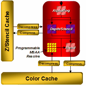 Among interesting innovations in ROPs we can note that AMD declares improvements in compression of Z/stencil buffers, up to 16:1 versus 8:1 in previous solutions, and up to 128:1 with MSAA 8x. Data from Z and stencil buffers are compressed separately, which must increase compression efficiency. The resolution threshold for compression has also been raised, as usual. While it was limited to 5 Mp, now this threshold is not specified. A lot of Z buffer optimizations have been added. Most of them are intended to accelerate stencil shadows in popular applications (DOOM 3, F.E.A.R., Unreal Engine 3, etc). We'll benchmark R600 performance in them in this article. New antialiasing modes
R6xx chips support multisampling with 8 samples maximum. To keep up with competitors with CSAA, the company introduced new Custom Filter Anti-Aliasing (CFAA) modes with up to 24 samples. These are special post processing modes intended to improve antialiasing quality with programmable subpixel layout, sampling outside pixel borders, and various sampling weights.
 CFAA chooses from four to eight neighboring samples outside a pixel depending on a mode. Even though these samples have lower weight than internal samples, this method will still blur the entire image. The more samples outside a pixel, the blurrier the image. The key advantage of this approach is improving antialiasing quality by updating drivers. Besides, developers will get control of multisampling in the next DirectX versions. Of course, the new chips also support all older features: adaptive antialiasing, temporal antialiasing, gamma correction for MSAA, etc. The major flaw of CFAA is that additional samples beyond pixel borders may deteriorate the resulting image quality. Remember the special antialiasing mode in NVIDIA cards, called Quincunx. It also used sampling outside a pixel and blurred image, so it was not very popular among most gamers. AMD has a more flexible approach, of course. Samples outside a pixel will have lower weight than internal samples, but blurring still cannot be avoided. Will it be a problem for sharp-eyed users? We'll check it up in the part devoted to render quality. In our opinion, another innovation in R6xx antialiasing is much more interesting. It's not finetuned in the current version of drivers - antialiasing with the edge detect adaptive filter. This method uses edge detection to filter the rendered image. Pixels with high frequencies (polygon borders and sharp changes between textures which usually need antialiasing) use higher-quality antialiasing with more samples, other pixels - with fewer samples. This approach resembles the one used in FAA mode in Matrox Parhelia. Theoretically, it must demonstrate excellent results both in terms of antialiasing quality and performance. It works in places where it's really necessary, it reduces texture noise, and shouldn't deteriorate details. But this is theory. We'll see it in practice in the quality section. 512-bit memory ring busOne of the obvious advantages of R600 is its 512-bit ring bus. It's the first GPU to support 512-bit memory access. Now the ring bus includes 64-bit channels connected with an internal 1024-bit bus (two 512-bit directions), there is no central hub. This solution scales well and provides very efficient bandwidth. It's over 100 GB/sec for the first video cards based on R600 with usual, not very fast GDDR3 memory. It may grow in future solutions, because the controller supports fast GDDR4 memory.
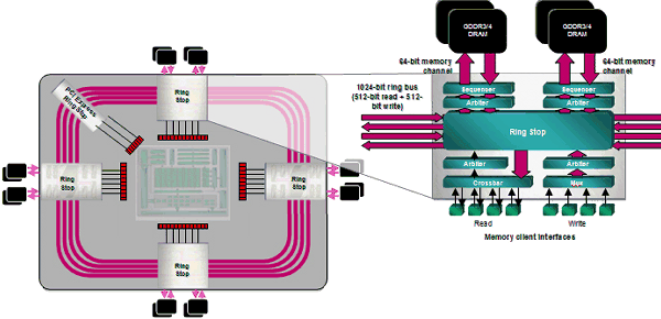 According to AMD representatives, the ring bus has been modified to increase its efficiency. Of course, such results can be obtained with a 384-bit bus as well (for example, NVIDIA GeForce 8800 Ultra), but it requires much more expensive and rare memory. On the other hand, 512 bits have a drawback - PCB gets more complex, and it becomes more expensive to assemble such cards. In return, higher bandwidth will show itself in higher resolutions, with high antialiasing levels, and HDR. In such modes we can expect RADEON HD 2900 XT to have a great advantage over competing solutions from NVIDIA. Programmable TessellatorOwing to R6xx's legacy (console GPU Xenos), all RADEON HD 2000 cards contain a programmable tessellator, a new unit for PCs. You can get the basic idea of tessellation in the following articles:
Tessellation is used to increase geometric complexity of models, that is to make complex models from low-polygon ones. Tessellation can reduce overheads on animation, increase model details at a small performance loss, improve LOD. A fully hardware solution allows developers to send data with a lower detail level to the GPU, then have them tesselated to a required complexity level, and apply displacement mapping (see the link above). It reduces the load on the CPU and the amount of data transferred along the buses.
Tessellation does not have a single algorithm, it can be done by several rules. There are several types of higher order surfaces: Bezier, N-Patches, B-Spline, NURBs, subdivision surfaces, which can be tessellated into polygons by a GPU. As R6xx is equipped with a programmable tessellator, it can be used for various algorithms, which gives 3D developers flexibility and control. AMD publishes the following block diagram of the pipeline:
 It's said that R6xx tessellator does not require new shader types in API, necessary vertex shaders can be written by developers. It's not clear how a usual vertex shader can do tessellation, but it's actually the problem of game developers. The programmable tessellator has great advantages. Tessellation can raise a geometry detail level of a scene without increasing the load on the buses and CPU. Tessellation is especially efficient in combination with displacement mapping. But this is theory. Practice is usually not that peachy. We have some questions as to how the tessellator can be used in various APIs (Direct3D 9, Direct3D 10, OpenGL). But the most important question is whether developers will use GPU features from only one vendor instead of two? Of course, games ported from Xbox 360 (with native support for tessellation) will profit from this feature, but what about other video cards? Improved CrossFire SupportSpeaking of features offered by new AMD solutions, we should also mention the improved support for CrossFire. All new GPUs do not require special master cards. At last, native support for CrossFire has been added to GPUs for all price segments, starting from this series. As in case of RV570-based cards, usual cards can be joined with a bridge, similar to those used for NVIDIA SLI. The new chips support the same rendering modes: Alternate Frame Rendering, SuperTile, Scissor, SuperAA. The highest resolution available in CrossFire modes is 2560×2048@60 Hz. The most interesting point in the description of improved CrossFire is that it supports more than two GPUs to render the same frame. It will be a pleasure to test this feature, when we have this opportunity. ATI Avivo HDThere are some improvements in multimedia features of the new GPUs. All R6xx GPUs contain special units: UVD (Universal Video Decoder) and AVP (Advanced Video Processor). ATI Avivo is not gone. Like PureVideo in NVIDIA cards, it's evolving, and now it has got a fashionable addon - ATI Avivo HD. The previous generation of video chips can accelerate only some video decode stages, the most resource-intensive stages are still up to the CPU to process. The new generation of GPUs is equipped with a dedicated unit to decode video (UVD), which does all the work: hardware statistic decode of VLC/CAVLC/CABAC, iDCT, motion compensation and deblocking (removing block artifacts), offloading the CPU and 3D pipeline of the GPU. The latter is especially useful for Windows Vista, which uses 3D features of video cards to draw Aero interface. The entire family of new GPUs support the improved technology. They offer hardware acceleration for decoding resource-intensive video formats H.264 and VC-1 with the highest bitrates. They are the main formats for Blu-ray and HD-DVD. Support for hardware-based video decoding is enhanced with the above-mentioned new units. They differ from the previous Avivo generations in hardware-based execution of statistic decode functions, especially important for modern video formats. The new ATI Avivo HD technology allows to decode all mentioned formats with resolutions up to 1920×1080 at 30-40 Mbps, all necessary features are supported by all GPUs of this series.
AMD publishes the following table to compare its GPUs with competitors:
 Unlike similar video processing units in NVIDIA G84 and G86, AMD solutions support hardware-based statistic decoding for VC-1 format. Like NVIDIA, the company publishes similar CPU load results. Software-based decoding of a HD DVD loads a modern dual-core processor by 80%, hardware-based decoding on prev-gen GPUs will load a CPU by 60-70%. And a fully hardware-based UVD solution loads a CPU just by 10%. So, all existing discs can be played back even by mid-range computers. We'll check it up in our future reviews. As for now, we can only take it at their bare word. Non-graphical computationsHuge performance of floating point math computations in modern video cards and flexibility of unified architectures have given an impetus to using GPUs to compute physics in games and more serious tasks: mathematical and physical modeling, economic and statistical models and computations, OCR, image processing, scientific graphics, and so forth. That's why all GPU manufacturers have recently paid much attention to non-graphical computations on video cards. ATI(AMD) has launched special cards based on RADEON X1900 (Stream Processor) with the R580 GPU and 1 GB of GDDR3 memory. The new chips certainly possess everything necessary to create such products. Their still higher floating point computing capacity can be used in many ways: to compute physics in games, to process media data (for example, to transcode from one format into another, to capture and encode HD video) and images, to recognize voice and images, for medical purposes (virtual endoscopy, interactive visualization), meteorology, fluid and gas dynamics, etc. Perhaps, the announcement of RADEON HD 2000 video cards will be followed by the launch of new R600-based "Stream Processor" products supporting floating point and integer operations, which appeared in the new architecture. They will use the significantly increased power of 320 stream processors. Here is an incomplete list of new features that appeared in R6xx chips, which are important for non-graphical computations: integer operations, support for 8192×8192 textures, unlimited shader length, unlimited memory for registers, a special command processor for reduced CPU overhead. In a small digression we again complain that we haven't seen real examples of hardware-based physics computations in games. We even don't want to publish pictures provided by GPU manufacturers again, because nothing has changed for common users - unfortunately, GPU is not used for non-graphical computations in modern games. Support for HDMI and other external interfacesOne of the anticipated solutions in HD 2000 cards is the built-in audio chip to support HDMI audio output. There is no more need in external audio and corresponding cables with the appearance of solutions based on R600, RV610 and RV630. No need to transfer an audio signal from the integrated solution to a motherboard or an external sound card. Besides, Vista Premium certification requires the audio section to be integrated and HDCP protected. This AMD solution supports the following 16-bit PCM data formats: 32 kHz, 44.1 kHz, and 48 kHz, as well as AC3 - compressed streams, such as Dolby Digital and DTS. It may be convenient to transmit video and audio signals along the same HDMI connector in many cases, as a single cable replaces a bunch of them. Interestingly, HD 2000 cards have no HDMI connectors, they are equipped only with DVI. They come shipped with a special DVI-to-HDMI adapter to output HDMI signal. It's also used to transmit audio data (it's a digital format, its bandwidth is large enough for video and audio), which cannot be done by usual adapters. The new adapters are compatible with usual DVI connectors without audio output. This new feature is really useful, but not always. It will be useful for Mid- and Low-End cards, which can be installed into small quiet barebone media centers. There is no point in buying a High-End video card just to watch video on a big HDTV display. Perhaps the built-in audio feature will make RADEON HD 2400 and HD 2600 popular among system integrators that assemble multimedia centers, because these solutions offer excellent video decoding features, as well as video/audio output along a single HDMI connector. Unlike NVIDIA GeForce 8800, all the new solutions from AMD support Dual-Link DVI outputs with HDCP support. They are similar to GeForce 8600 GTS here, which was the first video card with this feature. Top video cards are equipped with two DVI outputs that come with special DVI-to-HDMI adapters. And Low-End models use a conservative solution - one D-Sub and one DVI. The next part of this article will be dedicated to comparison of R600 performance with that of the competing NVIDIA solution. Unfortunately, there will be no tests of RV610 and RV630 so far. So we don't know the effect of reduced execution units in these GPUs on performance. Part 2. Graphics card features and synthetic benchmarksWrite a comment below. No registration needed!
|
Platform · Video · Multimedia · Mobile · Other || About us & Privacy policy · Twitter · Facebook Copyright © Byrds Research & Publishing, Ltd., 1997–2011. All rights reserved. |


