 |
||
|
||
| ||
On May, 10, Intel officially announced three new Pentium M models codenamed Dothan. According to Intel press releases, the new generation of CPUs (first marked as Processor Number) is made using the 90-nm process and the strained-silicon technology, which makes a reserve for further performance rise and energy consumption decrease. The Dothan core contains 140 mln transistors, which is almost twice as many as in the previous Pentium M Banias model, and has virtually the same die area (83.6 sq mm). It is supplied with a double "energy-saving" L2 cache memory size (2 MB) and also features a number of microarchitectural innovations. They include a modified register-access system and an equally modified data prefetch. The former increases register control efficiency at reading/writing variable length data, and the latter makes it more effective to select and load into the cache memory the data that the CPU is likely to need. This research is aimed at finding the answer if the new Dothan core is just a "90-nm Banias with a 2-MB L2 cache" or something more. For this purpose, we are going to use the recently announced version 3.1 of the universal RightMark Memory Analyzer benchmark. We will then compare Dothan test results with those of Banias, described in the article on the microarchitecture of Pentium III/Pentium M CPUs. Configurations of testbeds and softwareTestbed #1 (ASUS A6000Ne notebook)
Software
Testbed #2 (MaxSelect TravelBook Z4 notebook)
Software
CPUID characteristicsWe will start our research with the analysis of the announced values that are given out by the CPUID instruction. The focus of our attention will be on the parameters of the caches and the TLB, the low-level characteristics that are to be measured in this article.
To begin with, here are the basic characteristics of the actual Pentium M realisation, the Banias core.
And now, CPUID parameters of the announced Pentium M Dothan model.
The changes in the most important low-level parameters can't be called fundamental. The signature has changed both in the stepping (it has increased by one) and in the model number. The new core of the sixth Intel CPU family got number 13 at once (the previous real model number in this family, number 11, belongs to Pentium III CPUs on a Tualatin core). A rather unlucky number for a new core, but its hexadecimal representation looks much better (0xD) and is suggestive of the interpretation that the number is related to the first letter of the core's codename, Dothan. In respect of the cache/TLB descriptors, only one change has been made, and it concerns L2 cache of the CPU. At the moment, the descriptor's value (0x7D) is absent from Intel's official guide on CPU identification (document 241618-025, dated February 2004). However, it is easy to guess that analogically to the actual Banias model, it corresponds to an 8-way set-associative unified L2 D/I-cache with a 2-MB size and a 64-byte line length. But as usual, testing in RMMA will show what it's all like in reality. D-cache/RAM real bandwidth
Traditionally, we begin our testing with the real bandwidth of RAM and L1/L2 D-cache (test: Memory Bandwidth, presets: D-Cache/RAM Bandwidth, MMX/SSE/SSE2). We've got seemingly identical results using MMX, SSE, and SSE2 instructions for RAM access and therefore, we're giving you the general picture of the test with MMX instructions.
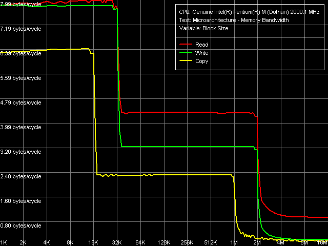
It's easy to see that Pentium M Dothan L2 cache really has a 2-MB size and its architecture is inclusive, which is typical of all Intel CPUs. In this particular case, it is not at all a serious shortcoming as doubling the data from the 32-KB L1 cache only takes 1.5 percent of L2 size. Now we'll estimate quantitatively performance of different levels of the platform's memory subsystem.
In read operations, the real bandwidth of L1 D-cache nearly reaches its maximum. Its 7.99 bytes per cycle still correspond to one 64-bit value sent per cycle from the CPU cache into the registers. In this respect, there's practically no difference between Dothan and Banias, as the latter, too, can read values from L1 D-cache with a nearly 100-percent efficiency. But the platforms differ greatly in terms of writing values from CPU registers into L1 cache. Banias shows a more effective writing from MMX registers (7.96 against 7.83 bytes/cycle), while Dothian leads in writing from SSE/SSE2-registers (7.88 against 7.52 bytes/cycle). Major differences can be observed in L2 cache. It is the very component of Pentium M CPU microarcitecture, that underwent changes being adjusted for the new core. Unfortunately, the characteristics became worse: L2 reading efficiency decreased by 5 percent, writing efficiency by 24 percent. We'll carry out a more thorough investigation into the work of L2 cache and L1-L2 bus a bit later. And now we'll examine the data on the real RAM bandwidth. Dothian has a somewhat lower efficiency of total RAM data reading (70.7 percent of the theoretical maximum vs. Banias's 81.6 percent), as well as of total writing (440 MB/sec, 16.5 vs. 22.5 percent). However, this result has no direct relation to the realisation of the CPU microarchitecture, as it is mostly dependent on chipset settings (memory timings, in particular) and the used RAM itself. Real peak RAM bandwidth
It's interesting to know the real peak bandwidth that is achieved by different means in practice. The maimxal real reading bandwidth can be estimated with the help of Software Prefetch, Block Prefetch 1 and 2, and a method that reads the whole cache lines instead of a total data reading. Here is the most representative picture that we received in Software Prefetch using MMX registers. 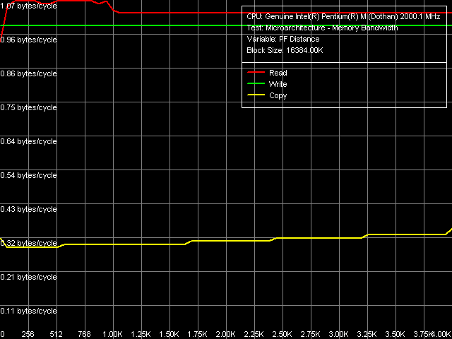
And to demonstrate the influence of a large L2 cache size, here are the curves of reading/writing the cache lines at a 4-16 MB data block size.
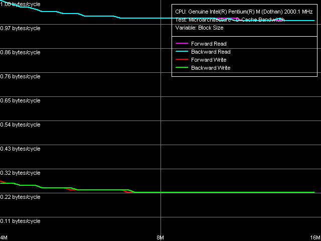 L2 influence is obvious: the curves acquire constant values only after 8 MB. It is no surprise, as a line-by-line reading/writing of a 4-MB data block is marked by 50 percent of the data hitting L2 cache.
Now let's get back to Software Prefetch readings. It shows its maximal effectiveness at the prefetch length from 64 to 960 bytes and reaches about 81 percent of PC2700 DDR theoretical bandwidth.
By the way, Dothan's realisation of Software Prefetch is very much different from Banias's.
Our previous article on the latter's microarchitecture shows that in Banias, Software Prefetch
reaches its maximum at the prefect length of 64 bytes and more, after which it stays on a constant level. Another major difference is the gain from using Software Prefetch: about 1.08 times in Banias and about 1.14 times in Dothan.
Thus, an important difference between Dothan and Banias microarchitectures is the modified Sofware Prefetch algorithm in the former one. We saw a similar picture in Prescott when testing Pentium 4 platforms. It's not improbable that Intel realised in its new Dothan core the same ideas that had been implemented in Prescott.
*the figures in brackets show the percentage of the theoretical limit for the given memory type We'll mention other methods, especially Block Prefetch 1 and 2 only in brief. There's no reason to dwell on them as they either bring an insignificant win (Block Prefetch 2) or even a loss (Block Prefetch 1). The line-by-line data read gives an equally small win on both cores. As for the relative figures (percentage of the theoretical limit), they are a little lower in Dothan than in Banias in all the cases. But it is quite natural considering the former platform has lower relative values of the average real reading bandwidth.
Now let's take a look at the data writes. As before, there are only two methods to optimise the writing: non-temporal store and line-by-line write. Despite the fact that Dothan is characterised by a lower average real writing bandwidth, the platform gains more from using non-temporal store: 4.50 times against Banias's 3.65. Thus, Dothan also shows progress concerning the non-temporal store algorithm. This progress has been presumably achieved by increasing the number or the sizes of the write-combine buffers.
*the figures in brackets show the percentage of the theoretical limit for the given memory type And still, we have no choice but to spoil this picture as we can't pay no attention to the data copy results received using the best optimisation variants together (Software Prefetch and Non-Temporal Store). Dothan's maximal real copying bandwidth is just 700.4 MB/sec (consequently, the full maximal real bandwidth is 1400.8 MB/sec, which makes up only 52.2 percent of the theoretical maximum). Banias has this shortcoming too: it is characterised by a 1372-MB/sec full maximal real copying bandwidth (64.3 percent of the theoretical limit). However, such effectiveness (2/3 of the theoretical one and lower) seems to be typical of all Pentium III CPUs, and their arcitecture has been inherited by the Pentium M family. Intel Pentium 4 and AMD K7/K8, on the contrary, show a very high efficiency in copy operations. D-Cache/RAM average latency
D-cache latency is the next important item we'll dwell on. To begin with, let's take a look at the curves from the D-Cache Latency test, preset D-Cache/RAM Latency.
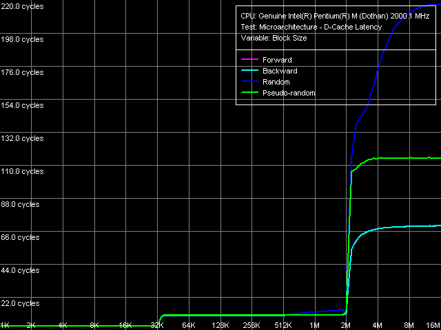
They show that Dothan, as well as its predecessor, is equipped with the Hardware Prefetch algorithm. Its effectiveness can be roughly estimated at 40 percent (comparing the values received from forward/backward serial reading and pseudo-random memory reading). By the way, the pseudo-random mode is a new option for RMMA. It was used in versions 2.5 and later, while Banias data were received from version 2.4 and so, it's impossible to estimate Hardware Prefetch efficiency in it using the proposed method. But still, let's take a look at the quantitative characteristics of D-Cache/RAM latency.
*The block size is 4 MB L1 D-cache latency remained equal to three cycles, which is encouraging (as you remember, the new Pentium 4 Prescott core surprised us with a double increase in L1 D-cache latency). At the same time, L2 D-cache average latency grew, though not dramatically, up to 10 cycles. Memory access latency on Dothan is much smaller: 35.0 ns (against 51.2 ns) at forward/backward reading and 87.9 ns (against 146.7 ns) at random reading of a 4-MB memory block. But then again, it can hardly be considered the credit of microarchitectural improvements as other platform components, such as the chipset and RAM play a certain role here too. Especially considering that the Dothan platform has a PC2700 DDR memory, while Banias has a PC2100 DDR. L2 D-Cache/RAM minimal latency
Now let's estimate a more important parameter — L2 D-cache/RAM latency. For this purpose, we'll use a traditional method and gradually unload the L1-L2 (L2-RAM)
bus by inserting voids (test: D-Cache Latency, presets: Minimal
L2 D-Cache Latency, Method 1 and Minimal RAM Latency, 4MB Block).
First of all, let's see how L2 cache latency changes.
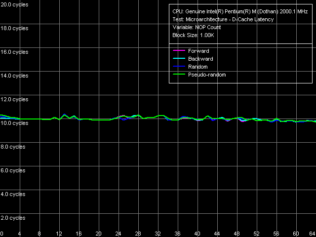
We see that it doesn't change at all, keeping its average value of 10 cycles.
Thus, a larger L2 size in Dothan caused the search for a needed line to increase by one cycle. Which is ridiculous comparing to what the company did in its new Pentium 4
Prescott core (L2 latency rose from 9 to 22 cycles there). Now let's look at the changes in memory access latency at bus unloading.
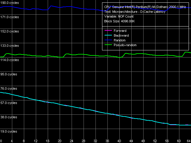
In this case, serial (forward and backward) reading modes enable
Hardware Prefetch to work at its maximal efficiency which results in a 24-cycle latency (12.0 ns). Banias has similar curves but a less effective unloading and a higher latency. Consequently, Hardware Prefetch is better realised in Dothan than in Banias. In respect of random and pseudo-random readings, it can be clearly seen that corresponding minimal latencies almost coincide with the average ones. And of course, we should also mention the familiar spiky look of the curves with a 20-NOP step corresponding to the CPU's multiplication factor.
It means that it is possible to swap with the memory at each cycle of the CPU's
100-MHz Quad Pumped system bus.
*The block size is 4 MB D-Cache associativity
Given below are the curves received in the D-Cache Latency test using the preset named L1 D-Cache Associativity.
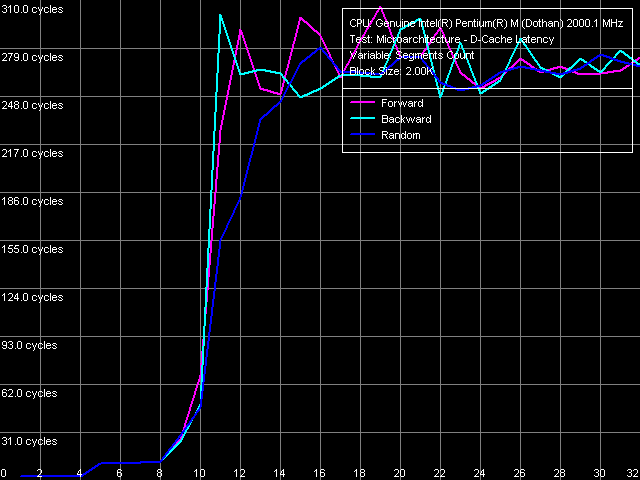 The graph clearly has two inflections that indicate L1 cache associativity equal to four (1-4 segments) and L2 cache associativity equal to eight (5-8 segments). Thus, there are no significant changes comparing to Banias (and Pentium III Tualatin as well). Intel has substantially enlarged L2 cache size but has taken no care of its associativity increase, which is not very good for a large cache like this. However, the picture is not new for Intel CPUs: for example, Pentium 4 XE (Gallatin), too, has a 2-MB cache with associativity 8 (although it's L3 not L2). What is more strange and what has not been the focus of our attention when testing Banias is that the announced L1 cache associativity (8, according to cache/TLB descriptors in CPUID) has nothing to do with reality. Of course, we could suppose that L1 cache has associativity 8 while L2 cache has 4 (which would be very strange for such a large cache). But this supposition is not corroborated by the L2 D-Cache Associativity test that executes a multi-segment reading of a 96-KB data block. The test results show that L2 cache associativity is 8 too. That means that the first jump of the curve above (area of 4 segments) really indicates L1 D-cache associativity equal to 4. L1-L2 D-Cache bus real bandwidth
Now we'll estimate the real bandwidth of L1-L2 D-cache bus using the D-Cache
Bandwidth test, preset L1-L2 D-Cache Bus Bandwidth.
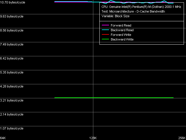
And we'll compare the results with those of Banias.
The bus precision is still equal to 128 bits (such bus has the peak bandwidth of 16.0 bytes/cycle). Its L2-L1 reading effectiveness has remained virtually unchanged (to be precise, it decreased by a negligible value) while writing effectiveness has considerably diminished (from 4.27 to 3.24 bytes/cycle, that is, by 24 percent). However, the result is not new for us, we had the same picture examining L2 cache efficiency in total data read/write operations.
By the way, it should be borne in mind that a 128-bit data bus typical for all
Pentium III/Pentium M CPUs is not effective enough equally for Dothan and
Banias, considering that the above-mentioned CPUs have a 64-byte L1/L2-cache line size.
Indeed, it would take as many as 4 CPU clocks to transmit this number of data bytes at the peak speed of 16 bytes/cycle. But as we know, L1 cache latency is 3 cycles, so even in ideal conditions, the requested line must be accessible at least with a 1-cycle delay.
The D-Cache Arrival test will show what happens in reality. Let's analyse how total latency of two accesses to the same line changes when the distance between the accesses increases from 4 to 60 bytes. For this purpose, we'll use preset L1-L2
Cache Bus Data Arrival Test 1, 64 bytes.
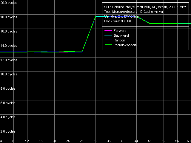 We've got exactly the same result that was in the case of Banias, except quantitative features (a 1-cycle difference corresponding to an increased L2 cache latency). Two-access latency remains minimal (13 = 3 + 10 cycles) with the second element offset up to 28 bytes inclusive, and then it increases by five cycles, and falls by one cycle if the offset goes on (up from 48 bytes). The result means that the requested 64-byte line is really not immediately accessible to L1 cache. I-Cache, decoding effectiveness
We're using the Decode Bandwidth to estimate the effectiveness of Dothan's I-cache, decoder, pipeline, and executable module. As usual, we got the most representative result decoding simple but "massive" 6-byte CMP instructions (preset L1 I-Cache Size/Decode Bandwidth, CMP
Instructions 3).
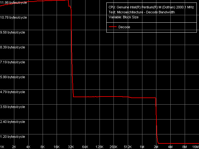
Decoding/execution from L1-I cache is as effective as 12 bytes/cycle, which corresponds to two instructions executed by two CPU's executable ALU modules.
Other instructions are given in the table below.
First of all, it should be noted that Dothan executable modules obviously have the same construction as they had in Banias. This is indicated by identical decoding speeds concerning various simple ALU instructions. It is essential that only a few of independent operations are executed at the maximal speeds on these CPUs. Indeed, such independent operations as SUB, XOR, and XOR/ADD are executed at one per cycle. And because the executable resources are all right (they are capable of executing NOP, TEST, and CMP instructions at the maximal speed of 2 operations/cycle), it is due to the CPU's inability to solve such complex false dependences. What is also essential is an extremely low execution speed concerning very simple CMP instructions that contain two "meaningless" prefixes (Prefixed CMP 1-4). Both CPUs execute it in four clocks, and unfortunately, the new Dothan core has no modifications in this respect. Instead, it just inherits the old Pentium III microarchitecture that was modified with SSE2 instructions in Banias. Besides, the new Dothan is marked by a lower efficiency of decoding/executing instructions from the unified L2 cache, which is manifest in decoding/executing massive instructions, such as CMP 3-6 (4.22 bytes/cycle vs. Banias's 4.36). However, the result fits our previous finds indicating a lower L1-L2 cache bus efficiency. I-Cache associativity
To measure L1-I/L2 cache associativity, we'll use the new test (that appeared in
RMMA 3.0 and later) named I-Cache Latency, and select preset I-Cache/RAM
Latency, Near Jump.
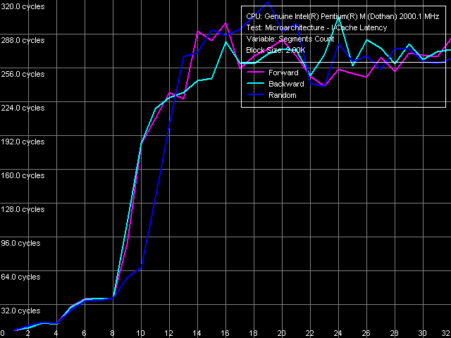 The conclusions we drew about L1 D-cache associativity equal to 8 can also be applied to I-cache. The test shows that L1 I-cache associativity is four (not eight as is stated in CPUID), and unified L2 I/D-cache has associativity equal to eight. D-TLB characteristics
According to the values of the cache/TLB descriptors given out by the CPUID function, the new Dothan
core has no changes in any of D-TLB and I-TLB parameters, such as size or associativity. These final tests will check it as well as estimate the impact of D-TLB/I-TLB miss on the values of L1-D/L1-I
cache access latency. To begin with, we'll use the D-TLB test, preset D-TLB Size.
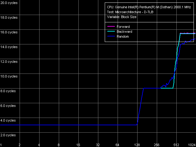 D-TLB size is really equal to 128 entries (observant readers could have estimated this parameter themselves if they had looked at the curve of random access latency in the area of L2: latency gradually increases at 512 KB and higher, which corresponds to 512 KB / 4 KB = 128 page entries. D-TLB miss is marked by a 5-cycle increase in L1 D-cache access latency, which is typical of all Pentium III CPUs, including Pentium M. The next jump (at 512 pages) is caused by the overfilling of L1 D-cache that can only contain 32 KB / 64 byters) = 512 lines.
To estimate D-TLB associativity, we choose preset D-TLB Associativity, 64
Entries, thus using only a half of the buffer.
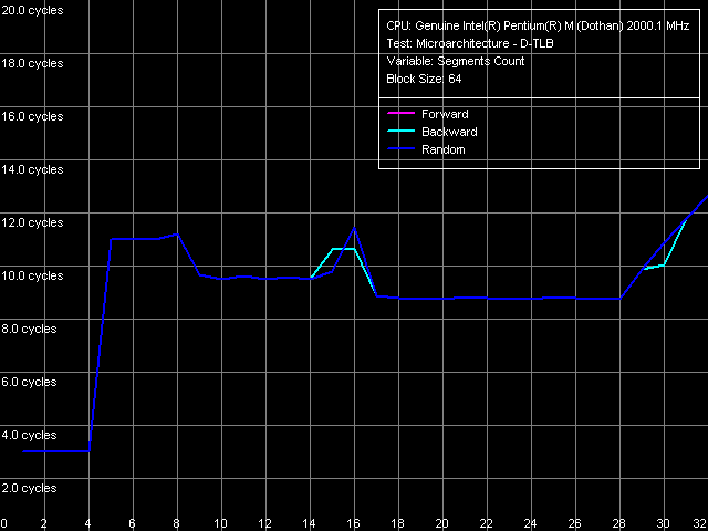 The curves show that D-TLB associativity is equal to four, and its exhaustion is marked by L1 D-cache latency increase to 9 cycles on average. The same picture was in Banias core testing. Thus, we can say that Dothan and Banias have absolutely identical D-TLB realisations. I-TLB characteristics
And finally, let's look at I-TLB realisation in the two cores. We will start with the buffer size estimation
(test: I-TLB, preset: I-TLB Size, Near Jump).
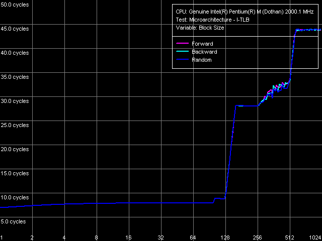 It is exactly the size that was announced (128 entries), and the miss costs L1 I-cache about 20 cycles. Also noteworthy is code chain reading latency at the beginning (given an I-TLB hit) that is, in fact, the time of the execution of one near jump instruction. It takes as many as 8 cycles against 2 cycles in Pentium III CPUs. However, Banias had the same characteristics, and consequently, they are typical of all Pentium M CPUs.
To estimate I-TLB associativity, we'll use preset I-TLB Size, Near Jump,
64 Entries.
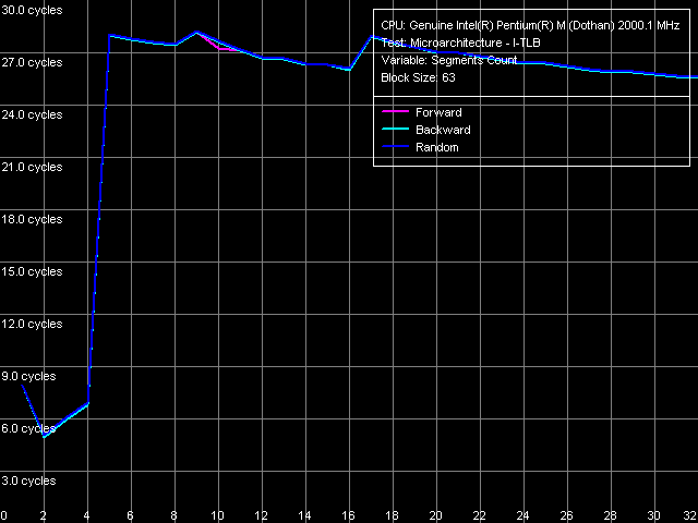 As was expected, Dothan's I-TLB asociativity equals four. Its exhaustion, as well as buffer overfilling, leads to L1 I-cache access latency increase to 27 cycles on average. These I-TLB characteristics coincide with those we had in Banias. Thus, I-TLB realisation, either, hasn't changed on the way from Banias to Dothan. ConclusionTo sum up, let's look at the main aspects of Dothan microarchitecture, that have been modified comparing to the Banias core. The first and foremost thing that meets the eye is a double L2 D/I-cache that now houses 2 MB. On one hand, it is good for the new core, but on the other hand, there is a number of drawbacks. The first one is that L2 associativity remains exactly the same (eight) as it was in Banias, which is clearly not enough for a large cache like that. A low effectiveness of such cache will be especially unfavourable for caching data (not necessarily large ones) that are allocated far from each other in the virtual memory. Another serious drawback of L2 cache realisation is directly related to the increased cache size and manifests itself in two closely connected effects: increased L2 access latency and decreased L1-L2 bus efficient bandwidth, especially in write operations. But still, these parameters are not nearly as bad as they were in the new Prescott core. Thus, the new 90-nm Pentium M implementation can be considered much more successsful than its 90-nm NetBurst fellow. Modified Software and Hardware Prefetch algorithms are another positive aspect. The former is manifest in an increased reading efficiency, the latter in a lesser serial memory access latency (which is used much more often than random access). However, the new core is not devoid of a number of imperfections typical of Pentium M CPUs in general. They include a rather ineffective large-size data copy (even if the best optimisation variants are used) and the absence of modifications concerning the pipeline and the executable modules. The latter drawback manifests itself in the CPU's inability to execute independent operations effectively and in a longer execution of near jump instructions (compared to Pentium III). That seems somewhat strange as in modern CPUs, branching prediction algorithms tend to become increasingly advanced on newer cores.
Nevertheless, the results allow us to say that the Pentium M Dothan core is something new and different from "just a 90-nm Banias with a 2-MB L2 cache". Therefore, its release can be called a very successful step forward made by Intel.
Dmitri Besedin (dmitri_b@ixbt.com)
13.05.2004
Write a comment below. No registration needed!
|
Platform · Video · Multimedia · Mobile · Other || About us & Privacy policy · Twitter · Facebook Copyright © Byrds Research & Publishing, Ltd., 1997–2011. All rights reserved. | ||||||||||||||||||||||||||||||||||||||||||||||||||||||||||||||||||||||||||||||||||||||||||||||||||||||||||||||||||||||||||||||||||||||||||||