 |
||
|
||
| ||
|
||
|
||
| ||
Appendix 1:
Hyper-Threading Effect
We continue the series of the low-level tests of platform's vital features with the universal RightMark Memory Analyzer. This time we are dealing with the Intel Pentium 4 based platform which is timed to the launch of the new 90-nm Prescott processor. This test will let us find out the most important changes brought into the NetBurst microarchitecture. We have selected three Intel Pentium 4 models (Northwood, Gallatin and Prescott) of the same core clock (3.2 Ghz), which let us compare them in the same conditions (the same core clock, chipset and memory type). Testbed and software
Testbed:
System Software and drivers:
Real D-Cache/RAM BandwidthFirst of all, we are going to estimate the real average bandwidth of the data cache and RAM in two access modes using MMX and SSE/SSE2 registers. Memory Bandwidth Benchmark, D-Cache/RAM Bandwidth, MMX Registers; SSE Registers; SSE2 Registers settings. SSE/SSE2 registers allow for a higher real D-cache/RAM bandwidth, with the results of SSE and SSE2 being identical. Here is a general picture of the real BW for SSE registers. Average real RAM bandwidth, Intel Pentium 4 Northwood Average real RAM bandwidth, Intel Pentium 4 XE Gallatin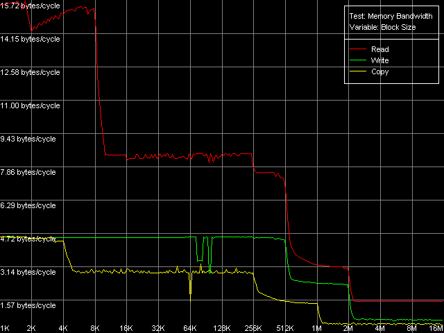 Average real RAM bandwidth, Intel Pentium 4 Prescott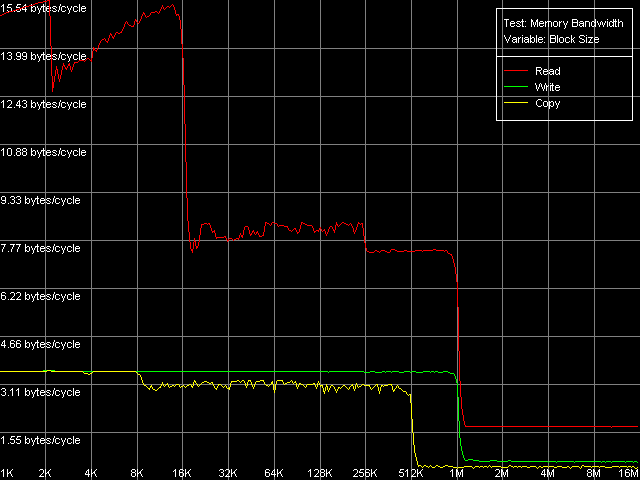 The diagrams of all three processors look obvious. They demonstrate two cache levels (L1 and L2) the size of which complies with the specification (8/8/16 KB L1, 512/512/1024 KB L2 for Northwood/Gallatin/Prescott respectively). The volume of both cache levels was doubled in the new 90nm Prescott processor compared to its predecessors (Northwood and Gallatin). Pentium 4 XE has one more d-cache level (L3) of 2 MB. In all cases the effective L2 cache bandwidth reduces at reading when crossing the 256KB point. It probably happens because of the empty D-TLB (which can fit only 64 entries, that corresponds to 256KB virtual memory addressing). It's also notable that the diagrams have bends that correspond to the size of L1, L2 (and L3) d-caches and it implies the inclusive architecture (as we saw in the previous tests, the exclusive d-cache of AMD K7/K8 CPUs behaves differently). Let's estimate the average real bandwidth of the d-cache L1, L2 (L3)
levels and RAM on the tested platforms.
The Intel Pentium 4 processors have much in common and certain differences. Thus, the effective BW of the L1/registers tandem is close to 8 bytes/clock (MMX) and 16 bytes/clock (SSE) in all cases, which means that only one value can be sent from the memory (64 and 128-bit, respectively) into MMX and SSE/SSE2 registers at one CPU clock. It was different for AMD K7/K8 processors: the real L1-LSU-registers bandwidth reached the maximum (13-15 bytes/clock) with MMX registers (transfer of two values per clock), while the effective BW shrank twice with the transition to the SSE registers (transfer of one operand at two CPU clocks). The L1 efficiency at writing didn't change with the transition from Northwood to Gallatin, but it dropped by 20-28% on Prescott. The L2 demonstrates effective reading both on Northwood and on Gallatin. Prescott, with its larger L1 and L2, changes the picture: the efficiency of reading into MMX registers increased by 7%, and that of reading into SSE fell down by 1%. The write efficiency regarding the same cache level is similar to that of L1 cache: the transition to the new Prescott microarchitecture made it fall down by 20-28%. Let's see whether there is any difference in RAM access operations. Its average real BW at reading is very close on Northwood and on Gallatin, since the third cache level doesn't make any effect here. At the same time, the new 90-nm processor demonstrates the growth of this parameters (by 13-27%), especially in case of MMX registers. It proves that the Hardware Prefetch algorithm was improved in the new Prescott architecture. We'll touch it later, when testing the RAM access latency. The real write RAM bandwidth increased even on Gallatin (by 39% on average, compared to Northwood) and hardly changed in the new microarchitecture (it even shrank by 5%). So, the new Prescott demonstrates a low efficiency of both d-cache levels at writing and an increased real memory bandwidth at reading. Maximum RAM BandwidthWe'll try to get the most from the memory subsystem, i.e. the maximum real memory bandwidth in read and write operations. For that purpose we will use the following methods of reaching the maximal real RAM bandwidth at reading:
And the following methods of reaching the maximal real RAM bandwidth at writing:
MMX and SSE/SSE2 registers will be used in all cases possible. Note that Prefetch/Non-Temporal store methods are realized in the Memory Bandwidth test and cache lines reading/writing methods are realized in D-Cache Bandwidth benchmark. Here are the curves obtained using Software Prefetch and SSE registers. Maximal real RAM bandwidth, Intel Pentium 4 Northwood Maximal real RAM bandwidth, Intel Pentium 4 XE Gallatin Maximal real RAM bandwidth, Intel Pentium 4 Prescott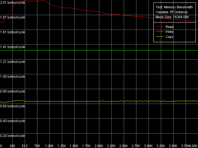
In the maximal real read RAM BW test the usage of MMX both on Northwood and on Gallatin is inferior to SSE/SSE2 (the scores of the latter ones are identical). Software Prefetch provides a good performance gain for all processor types. The maximal possible RAM BW is reached on Gallatin and Prescott , - they are equal to 6124.1 MB/s and 6493.4 MB/s. Gallatin allows for a higher real RAM BW as compared to Northwood, probably because the former has a relatively large additional L3 d-cache level of 2 MB. The memory reading efficiency in case of Software Prefetch both with MMX and SSE/SSE2 registers on Prescott is the same which means that Software Prefetch has a great potential on Prescott processors. Software Prefetch is much improved in the new Prescott and it virtually can reach 100% efficiency of the dual-channel DDR memory at reading. It's mentioned in the Prescott documentation. In particular, they mention that in the new NetBurst microarchitecture the Software Prefetch instructions can initiate both data loading from a new memory page (which lacked in the previous versions of Pentium 4) and loading of a respective page descriptor into D-TLB. Another vital enhancement is the Software Prefetch instructions caching by the processor's Trace cache in order to reduces expenses for their execution. The Block Prefetch methods are specific for AMD processors and we show their results just to make sure that they do not suit the Intel Pentium 4 family tested. They reduce the real RAM BW as compared to the average real RAM BW obtained without any optimizations. The cache lines reading methods provide close results on Northwood and
Gallatin which are approximately 19% higher than the average real RAM BW
at reading on these processors. By the way, the value 5950.4 MB/s achieved
in these methods on Northwood is its absolute limit unreachable with the
Software Prefetch because the latter is realized less efficiently. At the
same time, reading of the cache lines on Prescott is 2% better than the
usual full data reading with SSE/SSE2 registers.
Here, in all three cases the maximal real RAM BW makes 4290 MB/s which corresponds to 67% of the theoretical maximum dual-memory DDR RAM BW. It can be reached with the non-temporal store method on write-combining protocol. The fact that Prescott has a great number of store and write-combining buffers has no effect here - it's possible that the maximum real RAM BW depends on the chipset type used, i.e. a chipset type is the limiting factor. The results of the cache lines writing method are also unexpected. While the L2-RAM efficiency in reading is lower for Prescott (by 2-3%) than for Northwood/Gallatin, its writing efficiency is the highest on Prescott (higher by 12-17%). Nevertheless, the real RAM BW reached with this method is higher than the average (by 26-66%, depending one the CPU model), but it's still far from the maximum reached with the non-temporal method. D-Cache/RAM LatencyHere we expect to reveal the most unexpected features of the new NetBurst architecture of the 90nm Prescott. D-Cache Latency test, D-Cache/RAM Latency preset. Average latency, Intel Pentium 4 Northwood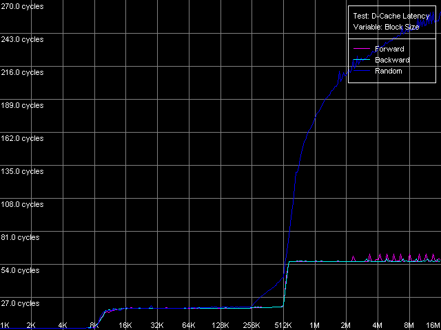 Average latency, Intel Pentium 4 XE Gallatin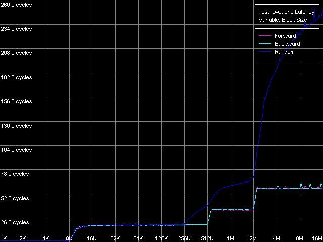 Average latency, Intel Pentium 4 Prescott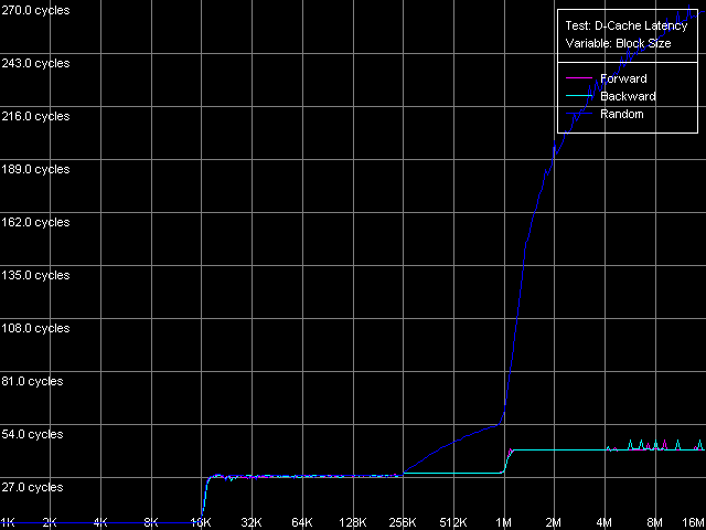 The overall picture is obvious for all three processors. The curves have clear zones that correspond to the L1 latency (up to 8KB unit for Northwood/Gallatin, and up to 16KB for Prescott) and to the L2 (up to 512 KB for Northwood/Gallatin and up to 1MB for Prescott). As expected, Pentium 4 XE excellently reflects its L3 d-cache up to 2 MB units. The bends at the points corresponding to L1, L2 (L3) prove the inclusive cache levels organization in these processors, including the L3 cache in Pentium 4 XE. Note that doubling of the whole 512KB unit of the L2 cache in the 2MB L3, which makes 25% of its size, is a great payment for simplicity of the cache bus organization (L1-L2 and L2-L3). As we know, AMD realizes a more complicated exclusive architecture of the L1-L2 levels in its K7/K8 processors protecting from unnecessary data even a 6.25% share (Opteron, Athlon 64), not to mention the 25% share (Athlon XP/MP) of the L2 d-cache. The random-access latency curves for all three Pentium 4 processors gradually grow up at the unit size of 256 KB and over. The first test of the average real L2 bandwidth showed a similar picture, and it happens because the D-TLB size of this processor type is pretty small and ensures effective addressing for only 256 KB (64 pages) of virtual memory. Such a small D-TLB size at the relatively big cache (1 MB L2 for Prescott and 2 MB L3 for Gallatin) is a bad disadvantage of NetBurst architecture of Pentium 4 processors. Note that in the new revision (Prescott) Intel neither increased the D-TLB size nor realized a two-level system for D-TLB typical of AMD K7/K8. That is why it's difficult to precisely estimate the L3 (Gallatin) and RAM random access latency; and we use the values obtained at the block size of 1 MB (L3) and 4 MB (RAM). Quantitative assessment of average latency of different cache levels/RAM
in different access modes.
*1MB block sizeNorthwood and Gallatin demonstrate similar latency. The L1 latency makes 2 clocks in all access modes, the L2 latency is 18.5 clocks on average. The L3 latency of Pentium 4 XE in forward and backward access modes is twice higher than the L2 latency and makes 35.5 clocks (and 61 clocks in the random access mode, but remember that it can't be measured precisely). Finally, the RAM latency is 57-58 clocks (17.6-18.0 ns) in the forward/backward access modes, which implies a good Hardware Prefetch algorithm. The random RAM access latency (with the same stipulation) is noticeably higher and makes 229 clocks (71.0 ns) for Northwood and 185 clocks (57.0 ns) for Gallatin. The lower RAM latency on the latter can be explained by the L3 cache level whose size allows covering up to 50% of memory accesses in this case. Surprisingly, the L1 latency for Prescott grows up to 4(!) clocks in all access modes (it's higher than that of all other modern processors), the L2 latency grows up to 28.5 clocks. However, the Hardware Prefetch algorithm is improved in the new architecture of the 90nm Pentium 4. The forward/backward RAM latency drops to 41 clocks (12.7 ns), i.e. by 39% as compared to the previous Pentium 4 models. At the same time, the random RAM access remains at the level of Northwood and makes 225.5 clocks (69.8 ns). Minimal L2/L3 D-Cache/RAM LatencyIn this test we will load the CPU cache bus with NOPs. The diagrams are drawn for D-Cache Latency test with Minimal L2 Cache Latency, Method 1 preset. Minimal L2 latency, Intel Pentium 4 Northwood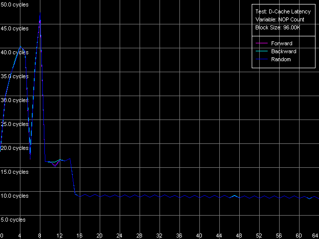 Minimal L2 latency, Intel Pentium 4 XE Gallatin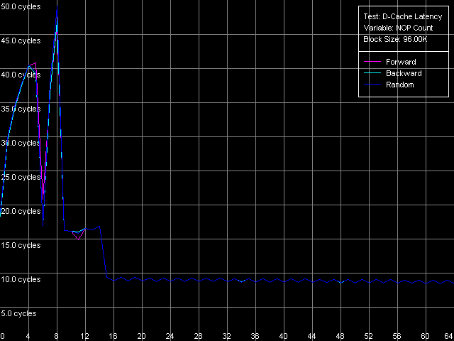 Minimal L2 latency, Intel Pentium 4 Prescott In case of Northwood and Gallatin 15 NOPs (OR EAX, EDX, 0.5 clocks runtime) are enough to reach the minimal L2 latency equal to 9 clocks. In case of Prescott the bus doesn't get unloaded irrespective of the number of NOPs (the execution of which is twice as high and makes one core clock), and the minimal latency can't be reached. Nevertheless, there's a certain minimum at 2 NOPs which makes 24 clocks (a bit lower than the average latency). The changes in the NetBurst architecture don't bring any benefit to Prescott. We have no choice but to use another bus unloading method specially developed for processors which support speculative data loading (though it makes no good for measuring latency). Let's look at the results for all three processors. Minimal L2 latency, Method 2, Intel Pentium 4 Northwood Minimal L2 latency, Method 2, Intel Pentium 4 XE Gallatin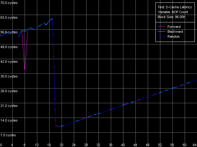 Minimal L2 latency, Method 2, Intel Pentium 4 Prescott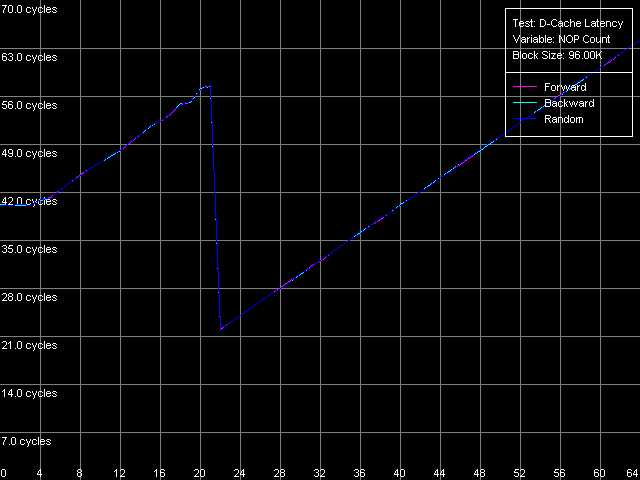 Northwood and Gallatin demonstrated the minimal L2 latency of 9 clocks in case of 18 NOPs (which corresponds to 9 core clocks, as expected). In case of Prescott the minimum equals 22 clocks at 22 NOPs (and taking into account that each of them takes 1 processor clock, the result is 22 clocks). So, the minimal L2 latency for Prescott makes 22 clocks. Since one of the processors has the L3 cache let's estimate its minimal latency as well. Presets: Minimal L2 Cache Latency (Method 1, 2), the block size is increased up to 1024 KB. 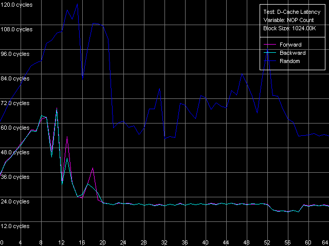 The minimal L3 latency can be easily reached at 20 NOPs in the forward/backward access modes and makes 20 clocks (though it's not clear why it falls down to 17 clocks at 53-58 NOPs). The minimal L3 random access latency is a bit higher and makes 52.7 clocks, which is nevertheless lower than the average value. Let's estimate the minimal RAM latency for all processors. There's some difference between the processor types though the chipset and memory type are the same. Minimal RAM latency, Intel Pentium 4 Northwood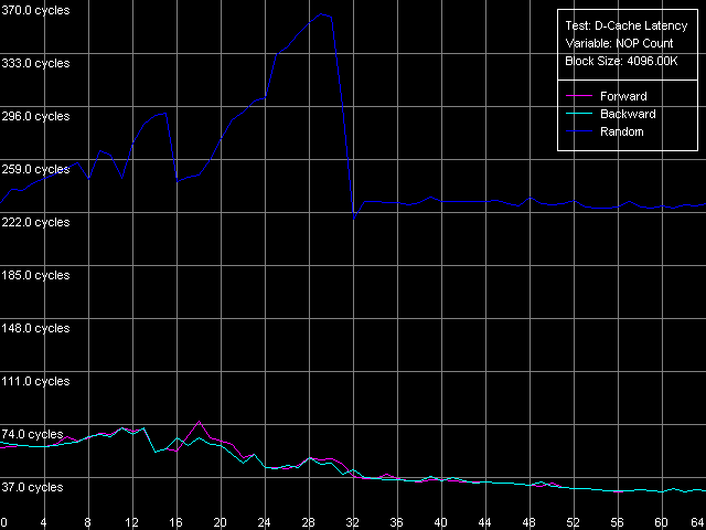 Minimal RAM latency, Intel Pentium 4 XE Gallatin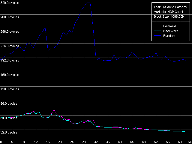 Minimal RAM latency, Intel Pentium 4 Prescott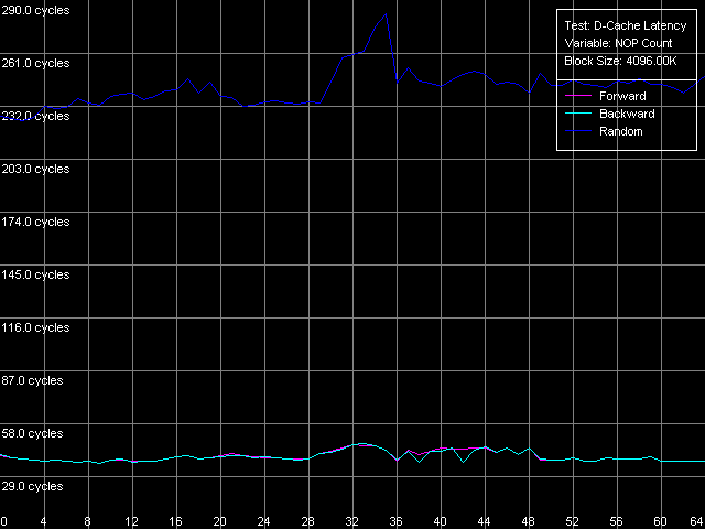 The first two processors behave similarly. The minimal RAM latency reached
in the forward/backward access modes is 27.3-27.6 clocks (8.4-8.5 ns).
In the random mode it makes 218 clocks (67.4 ns) on Northwood and 184 clocks
(57.0 ns) on Gallatin. On the latter processor it hardly differs from the
average value (185 clocks). The minimal latency in the forward/backward
modes on Prescott makes 36 clocks (11.2 ns), which is 31% higher compared
to the previous models. It seems that the Hardware Prefetch is specially
optimized for "dense" memory accesses that go without any gaps, while on
the earlier Pentium 4 versions the Hardware Prefetch likes inserting NOPs
between two memory accesses. Besides, it's quite possible that Prescott
has something wrong with the mechanism of loading the bus with NOPs, at
least because this method doesn't allow reaching the minimal RAM latency
in the random access mode - in our test it makes 224 clocks (69.3 ns),
while the average value makes 225.5 clocks, i.e. higher by 1.5 clocks.
* the parentheses contain the values obtained using Method 2. D-Cache AssociativityD-Cache associativity is not less important than its size or latency. This time we expect surprises rather from Northwood and Gallatin than from Prescott. D-Cache Associativity preset in D-Cache Latency test. Cache associativity, Intel Pentium 4 Northwood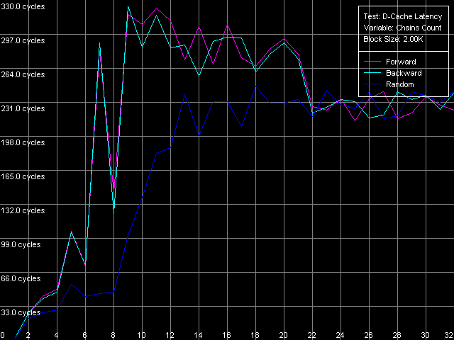 Cache associativity, Intel Pentium 4 XE Gallatin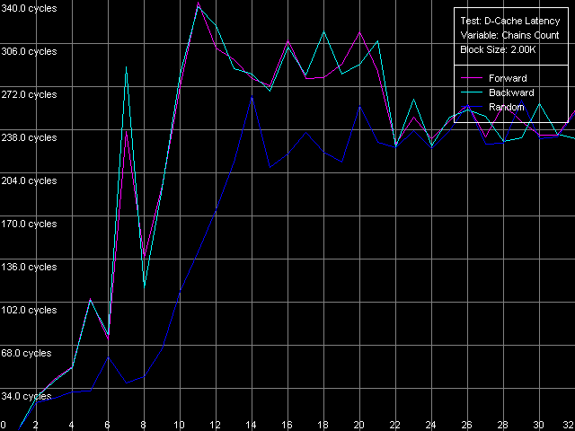 Cache associativity, Intel Pentium 4 Prescott The results are hard to interpret (as compared to AMD K7/K8 which always look perfect!). Nevertheless, all three Pentium 4 have two zones, which are well seen especially in the random access modes. The first point corresponds to the L1 cache whose associativity equals 1 in our test. The second zone includes up to 8 chains, it corresponds to the L2 cache associativity of 8. The fact that the L1 cache associativity is 1 is an unexpected result. Note that RightMark Memory Analyzer measures associativity by reading cache lines from "bad" memory addresses which are offset relative each other by 1 MB and over. It means that the L1 cache of all three Pentium 4 processors can't be effectively associated with more than one memory line of such addresses. That is why its real efficient associativity is equal to 1. Such result can't be considered a disadvantage of the test technique because the L2 cache reveals its real associativity (8-way set associative). The specified L1 associativity equal to 4 (Northwood, Gallatin) or 8 (Prescott) can be reached only in special access conditions. The L1 cache reveals its specified associativity only within its own size (each L1 cache line of the Prescott processor of 16 KÁ can be associated with 8 RAM lines which are offset by 16/8 = 2 KB relative each other). Real L1-L2 and L2-L3 Bus BandwidthThe Pentium 4 processors have a very wide 256-bit bus between L1 and L2 d-caches. Let's see whether it's really that effective and whether it remains the same in the NetBurst revisions. D-Cache Bandwidth test, L1-L2 Cache Bus Bandwidth preset. Real L1-L2 Bus Bandwidth, Intel Pentium 4 Northwood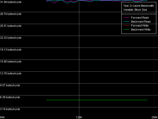 Real L1-L2 Bus Bandwidth, Intel Pentium 4 XE Gallatin Real L1-L2 Bus Bandwidth, Intel Pentium 4 Prescott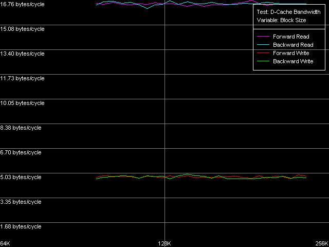 The bus efficiency for Northwood and Gallatin at reading is really high - it's equal to 31.89 bytes/clock, which makes 99.6% of the theoretical limit. At the same time, it's much lower at writing - 5.16 bytes/clock, which is only 16% of the theoretical maximum (we can consider that its real write bandwidth is only 64 bits). The L1-L2 bus efficiency of the 90nm Pentium 4 Prescott is twice lower compared to the previous models - to 16.76 bytes/clock (the efficiency makes 52.3%). Since this value is higher than 16.0 bytes/clock we can't affirm that the L1-L2 bus was halved to 128 bits. It looks like that the 256-bit bus was purposely slowed down. Unfortunately, the D-Cache Arrival test that allows estimating various peculiarities of the data bus organization is useless here - at 4 access latency clocks the whole lot of 64 bytes can be successfully transferred to L1 from L2 (a whole line) even in case of the 128-bit bus. I can say that by making the L1 access latency twice slower Intel masks other disadvantages of its new Prescott processor, in particular, the effective L1-L2 bus bandwidth. The effective L1-L2 bus bandwidth at writing also drops down in Prescott, though not that noticeably as at reading. 4.92-4.97 bytes/clock is only 4-5% lower than the value reached by the previous Pentium 4 models. As we mentioned in our previous review, AMD K7/K8 processors having the exclusive L1-L2 architecture have a much more effective L1-L2 bus bandwidth at writing cache lines. Since we have the Pentium 4 XE with a L3 d-cache let's estimate the effective L2-L3 bus bandwidth. L1-L2 Cache Bus Bandwidth preset with the following parameters:
As we can see, the L2-L3 bus in Pentium 4 XE has 64 bits. Its reading efficiency
is 6.05 bytes/clock (75.6%), and the writing one makes 4.67 bytes/clock
on average (58.4%).
Trace Cache, decode efficiencyOne of the most interesting elements of Intel's NetBurst microarchitecture is a special processor instruction cache called Trace Cache. It stores the results of operation of the instruction decoder in microops (up to 12000 uop inclusive), not the individual bytes that the x86 instructions consist of, like it takes place in traditional models of the L1i cache, and features some other advantages. One of the consequences of such cache architecture is that its size depends on a type of instructions used. Let's consider an example that allows reaching the maximal effective Trace Cache size and a high instruction decode speed. I-Cache test, L1i Size / Decode Bandwidth, CMP Instructions 3 preset. Instruction decode, Intel Pentium 4 Northwood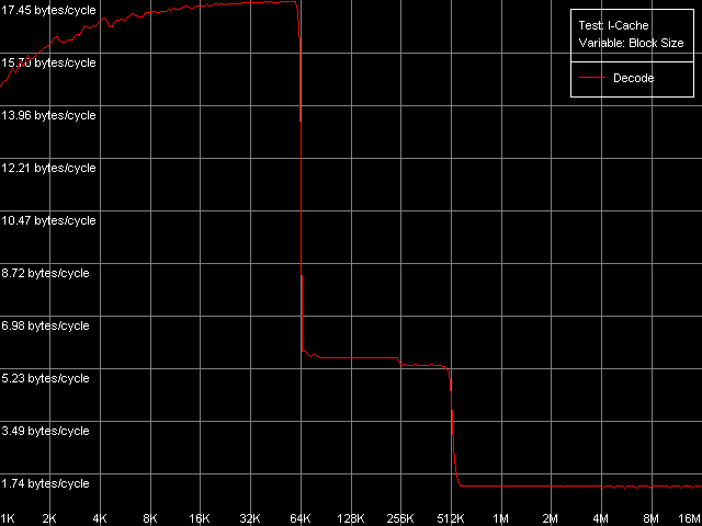 Instruction decode, Intel Pentium 4 XE Gallatin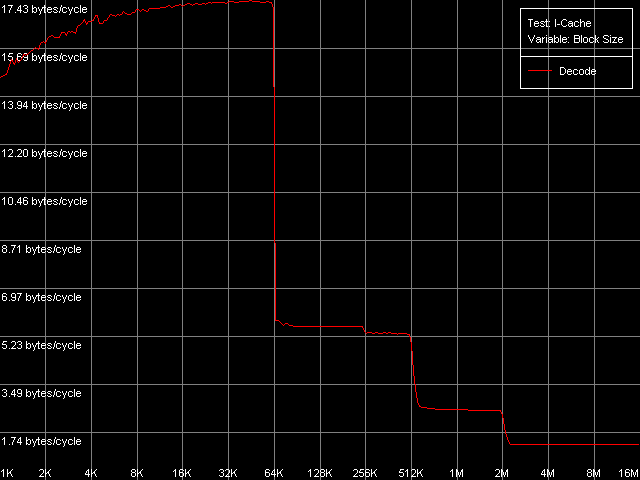 Instruction decode, Intel Pentium 4 Prescott All three processors reach a considerable effective Trace Cache size equal to 63 KB (10,500 uop). When this size gets exceeded the code is swapped from the L2 cache which is able to cache both data and code. The L3 cache of Pentium 4 XE is also able of it. At the code block size of 256KB and over the code execution rate falls down. The same behavior is demonstrated by the relatively small TLB, I-TLB, which has the same size (64 entries, 256 KB virtual memory addressing). Finally, we can see that the cache levels have an inclusive organization in this case, i.e. when caching the code instead of data. We carried out some additional tests using independent and dependent ALU operations to get more info about the Trace Cache and decoder of the processors. Decode efficiency, Pentium 4 Northwood
* 2 uops Decode efficiency, Pentium 4 XE Gallatin
* 2 uopsAs usual, we will start with Northwood and Gallatin processors and then proceed to Prescott. The Trace Cache size doesn't exceed 11000 uop in all cases, which implies that it has some reserve of 1,000 uop for service needs. The maximum rate of execution of simple instructions from Trace Cache reaches 2.9 instruction/clock. And it's limited by the processor's execution unit (whose limiting speed is 3 uop/clock), rather than by the rate of swapping of instructions from Trace Cache, when converted into the x86 instruction size (the execution rate reaches 17.44 bytes/clock and over). In this aspect the Pentium 4 CPUs look superior than AMD K7/K8, where the rate of execution of large x86 instructions was limited by the instruction swap rate from L1i into the CPU's execution unit (16 bytes/clock at most). As to the independent instructions, the XOR and TEST demonstrate that their limiting rate of execution is equal to only two ops per clock, identically to the dependent LEA/MOV/ADD/OR. It's probably caused by the fact that these instructions can be executed only in one of two FastALU units. Supplement of ADD to XOR (XOR/ADD) increases the execution rate up to the limiting value of 2.9 bytes/clock. CMP 6 code consists of repeating CMP EAX, 0x7FFFFFFF instructions. Such operation, as you can see, consists of two uops, in contrast to all other cases. And its efficient rate of execution, converted into x86 operations, is twice lower (1.46 bytes/clock). The results of testing the code containing CMP instructions with two "useless" prefixes are also of much interest. The increased execution rate (up to 23.2 bytes/clock), and the apparently reduced effective size of Trace Cache at decoding of such instructions makes us think that the "useless" prefixes are clipped by the x86 instruction decoder before a respective uop hits the Trace Cache. In such assumption the effective Trace Cache is not smaller as compared to storing CMP instructions (10,500 uops). At the same time, usage of the Prefixed CMP 4 ([0xF3][0x67]CMP EAX, 0x7FFFFFFF) code doesn't make our assumption entirely true. If we assume that the prefixes get cut off before the instruction hits the Trace Cache, and the very 32-bit CMP instruction is divided into 2 uops, the effective Trace Cache size gets equal to 14,700 uops, which is greater than the specified value of 12000. That is why the real situation is probably much more complicated than we thought. As to swapping of instructions from the uniform L2 code/data cache, the outcome depends a lot on the type of instructions. They are swapped at the rate of about 1 instruction/clock irrespective of what the L2 cache allows for. Only Prefixed CMP instructions are swapped from L2 at a lower rate - around half an instruction per clock. As you can see from the table, the code can also be swapped from the L3 cache of Pentium 4 XE (Gallatin). In this case the code execution rate seems to be limited by the speed parameters of this cache level because it's limited by some magical value of 2.64 bytes/clock (for instructions of 4-8 bytes). Decode efficiency, Pentium 4 Prescott
* 2 uopsNow let's look at the NetBurst architecture of Pentium 4 Prescott. The Trace Cache remains the same concerning independent operations. Only the speed of execution of microops reduced but it's the fault of the longer pipeline. The performance falls down by 1.7 (for the simplest operations like NOP and SUB) to 12.4% (long CMP and Prefixed CMP). XOR and TEST behave similarly - they need to be diluted by other ALU operations to reach the peak speed. That is why the ALU organization remains approximately the same. The dependent instructions like LEA/MOV/ADD/OR are executed at the speed of only 1 operation/clock (the fact that OR works similarly was clear yet in the minimal L2/RAM latency test). That is why we couldn't even estimate the effective Trace Cache limit because their execution speed from L1i and L2 is the same and equals 2 bytes/clock. On the other hand, the latency of execution of Shift and Rotate instructions has dropped to 1 clock against 4 clocks on the previous-generation Pentium 4 CPUs. Let's get back to prefix clipping, especially because RightMark Memory
Analyzer features a special test that estimates efficiency of decoding/execution
of x86 NOP with an arbitrary number of prefixes [0x66]. Prefixed NOP
Decode Efficiency preset.
As the "useless" prefixes increase in number on all three processors the speed of execution of such x86 instruction linearly grows up, up to 41 bytes/clock. At the same time, if we convert the value obtained into the real number of NOPs, we will get a typical speed of NOP execution (2.7-2.9 operations/clock, in parentheses), which marginally decreases when the number of prefixes grows up. Therefore, the NetBurst decoder is really able of separating "useless" prefixes yet when generating microops, right before they get into the Trace Cache. Finally, we have to estimate associativity of the L1i cache (Trace Cache) and L2 cache when executing the code from the latter. I-Cache Associativity preset. Instruction cache associativity, Intel Pentium 4 Northwood Instruction cache associativity, Intel Pentium 4 XE Gallatin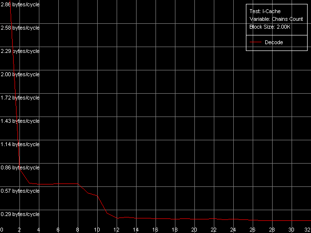 Instruction cache associativity, Intel Pentium 4 Prescott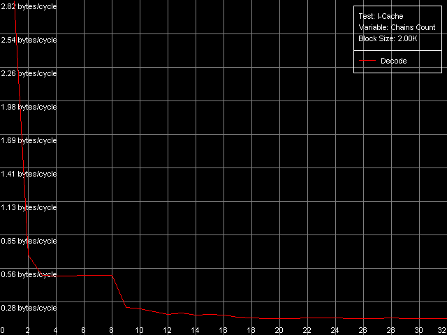 Northwood and Prescott show that the Trace Cache associativity is equal to 1, while the instruction/data L2 cache has it equal to 8 (exactly such value was obtained when we estimated the data cache associativity). The situation with Gallatin is more vague as it has an additional cache level the associativity of which at least doesn't exceed that of the L2 cache. D-TLB featuresFirst of all we are going to estimate its size which, judging by our numerous conclusions, must consist of 64 entries. D-TLB Size preset. D-TLB size, Intel Pentium 4 Northwood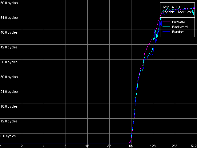 D-TLB size, Intel Pentium 4 XE Gallatin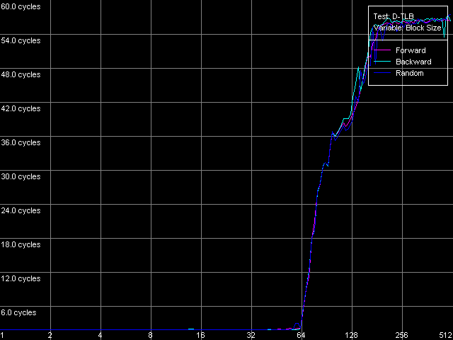 D-TLB size, Intel Pentium 4 Prescott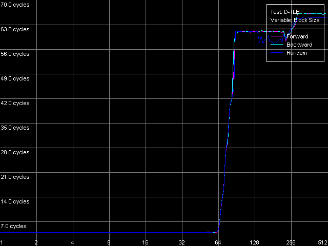 The D-TLB is single-level and the size of its single level is 64 entries (memory page descriptors) on all three processors. But the D-TLB miss costs a lot (from the standpoint of processor clocks). The L1 latency in case of the D-TLB miss makes some 57 clocks (Northwood, Gallatin) and 60-67 clocks on Prescott. The picture on AMD K7/K8, even in case of L2 D-TLB miss, is much better - the L1 latency doesn't exceed 30-36 clocks. Now we are going to estimate the D-TLB associativity. D-TLB Associativity, 32 Entries preset. D-TLB associativity, Intel Pentium 4 Northwood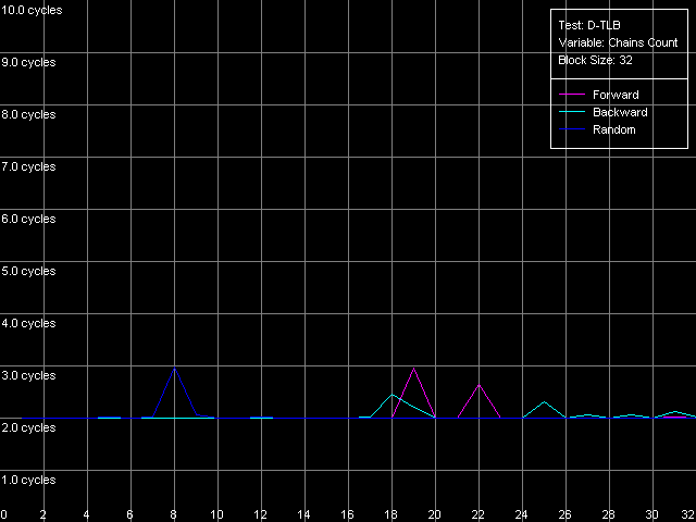 D-TLB associativity, Intel Pentium 4 XE Gallatin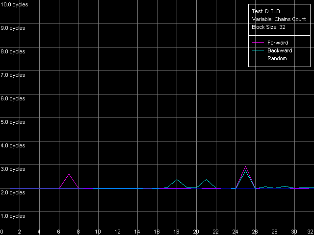 D-TLB associativity, Intel Pentium 4 Prescott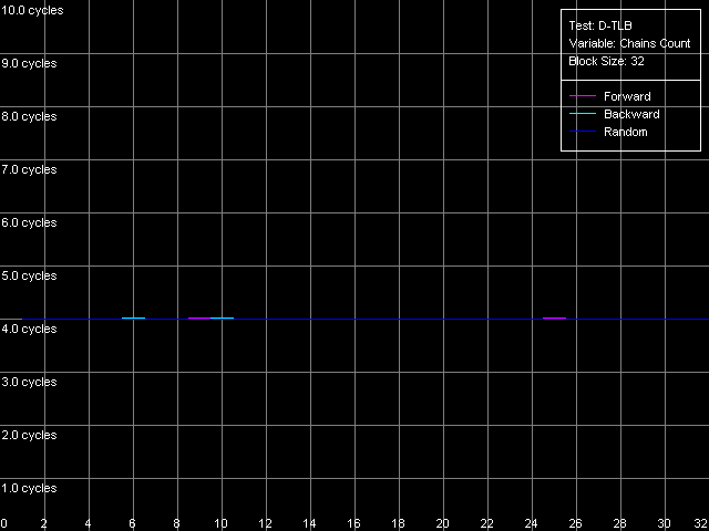 In all three processors the only D-TLB level is fully associative. I-TLB featuresLet's measure the TLB characteristics, like we measured the D-TLB. The I-TLB size was already partially discussed when we tested the Trace Cache, and we saw that the decode efficiency falls down when the code block size exceeds 256 KB. That is why we assume that the I-TLB in the Pentium 4 processors also contains only 64 entries for addressing 4KB virtual memory pages. Let's check it with I-TLB test, I-TLB Size preset. I-TLB size, Intel Pentium 4 Northwood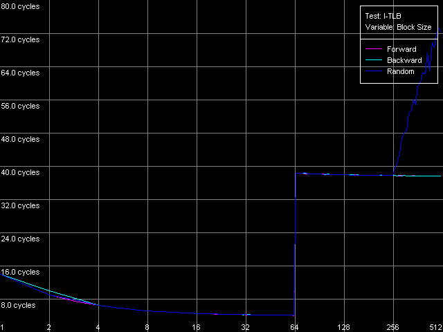 I-TLB size, Intel Pentium 4 XE Gallatin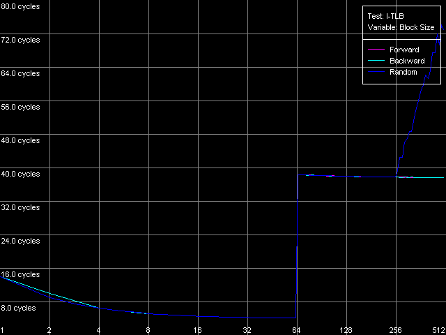 I-TLB size, Intel Pentium 4 Prescott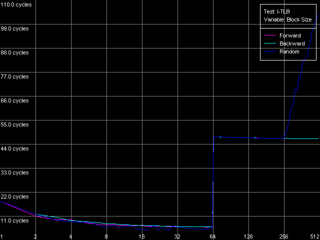 So, the I-TLB size on all three processors is really equal to 64 entries of virtual memory page descriptors (256 KB). The I-TLB is as expensive as the D-TLB - the latency at executing the code when "jumping" over the virtual memory pages increases up to 36 clocks for Northwood/Gallatin and 44 clocks for Prescott, when the I-TLB size is exceeded. I-TLB Associativity, 32 Entries preset. I-TLB Associativity, Intel Pentium 4 Northwood I-TLB Associativity, Intel Pentium 4 XE Gallatin I-TLB Associativity, Intel Pentium 4 Prescott So, the I-TLB, like D-TLB in these processors, is fully associative. Neither D-TLB nor I-TLB have any structural changes in the NetBurst microarchitecture realized in the 90nm Pentium 4 Prescott processors. ConclusionI must say that the new microarchitecture of Prescott makes a very complicated impression. On one hand, it features the improved Hardware and Software Prefetch support allowing for the higher maximum real memory bandwidth. There are some more pleasant facts about it like the lower latency of execution of Shift and Rotate instructions (1 clock vs 4) and the new SSE3 SIMD instruction set which will be studied separately. On the other hand, the L1/L2 cache access latency got higher, the effective bandwidth of the bus between these two cache levels is almost twice greater, the latency at executing some instructions has grown up. It looks like the NetBurst potential is held back, for example, to make the future Pentium 4 processors with the Tejas core look much better than the Prescott. Intel will certainly kill all those constraints. But we will carry out the low-level tests of the Tejas to reveal all the key changes of the NetBurst architecture, like we did it today with the Prescott processor. Appendix 1: Hyper-Threading effectIn this appendix we try to estimate whether the Hyper-Threading technology
(its enabling/disabling in BIOS) has an effect on any low-level parameters
of Intel Pentium 4 platforms, and what effect if any. The difference
in values of the cache/TLB descriptors obtained with CPUID function
(EAX = 2) on Intel Pentium 4 CPUs made us carry our this small investigation.
Actually, the difference was noticed in one descriptor that controls
I-TLB.
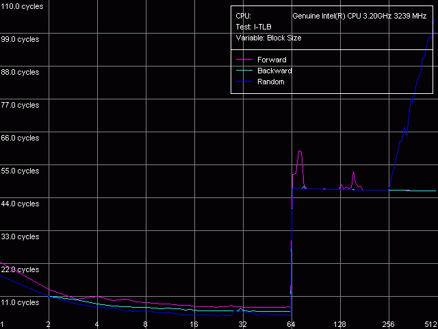
So, we ran I-TLB test (I-TLB Size preset) realized in RMMA v2.5. The test scores are identical for Northwood and Prescott - below are the diagrams drawn for the latter. I-TLB Size, Intel Pentium 4 Prescott, HT on
 I-TLB Size, Intel Pentium 4 Prescott, HT off
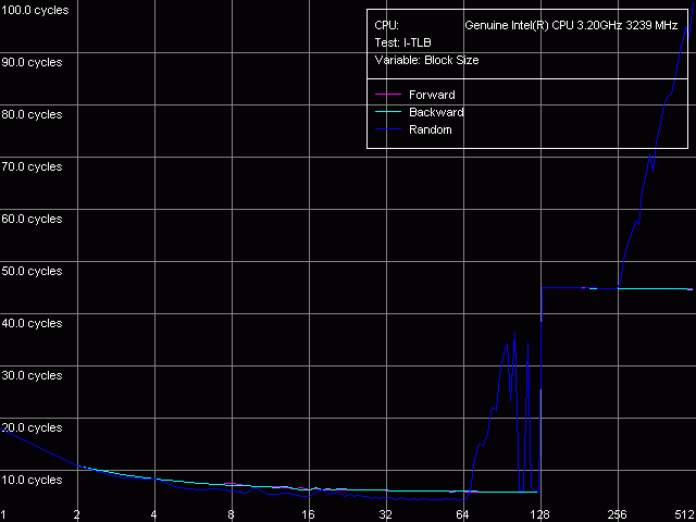 The I-TLB gets twice smaller with Hyper-Threading enabled, but its miss costs equally in both cases (the latency grows tenfold). So, Hyper-Threading as if halves this buffer so that each of two logical processors could have its own half. Using Intel's terminology, I-TLB can be referred to the partitioned type of CPU resources. According to Intel, most various buffers realized in the NetBurst microarchitecture are partitioned, such as microops queue buffers (in the Trace Cache field), renamed registers buffers (each logical CPU needs a separate set of registers), a reorder buffer, and load-store buffers. Note that I-TLB is not mentioned though its partitioning is well seen. Intel says that partitioning of such buffers is intended to minimize downtime of one logical CPU if the other gets stuck because of a miss (cache miss, wrong branch prediction, instruction dependence etc.). At the same time, the analysis of the cache descriptors and the D-TLB tests (D-TLB Size preset) does not show the difference in this buffer size when enabling/disabling Hyper-Threading - it remains equal to 64 entries in both cases, i.e. when Hyper-Threading goes on it becomes shared for both logical CPUs. Most CPU resources become shared with enabling Hyper-Threading in order to increase efficiency of dynamic utilization of a given resource. Processor caches and all execution resources are among them. As to D-TLB, which (as we found out) is shared, the documentation says that its entries in this case contain the logical CPU identifier. The results of all other RMMA tests didn't reveal any noticeable
difference in other vital low-level CPU parameters with enabling/disabling
Hyper-Threading, provided
that the Pentium 4 CPUs were tested with Hyper-Threading only in the
single-thread mode, i.e. when secondary processes create the minimal
load on the system.
Dmitry Besedin (dmitri_b@ixbt.com)
Write a comment below. No registration needed!
|
Platform · Video · Multimedia · Mobile · Other || About us & Privacy policy · Twitter · Facebook Copyright © Byrds Research & Publishing, Ltd., 1997–2011. All rights reserved. | ||||||||||||||||||||||||||||||||||||||||||||||||||||||||||||||||||||||||||||||||||||||||||||||||||||||||||||||||||||||||||||||||||||||||||||||||||||||||||||||||||||||||||||||||||||||||||||||||||||||||||||||||||||||||||||||||||||||||||||||||||||||||||||||||||||||||||||||||||||||||||||||||||||||||||||||||||||||||||||||||||||||||||||||||||||||||||||||||||||||||||||||||||||||||||||||||||||||||||||||||||||||||||||||||||||||||||||||||||||||||||||||||||||||||||||||||||||||||||||||||||||||||||||||||||||||||||||||||||||||||||||||||||||||||


