 |
||
|
||
| ||
|
||
|
||
| ||
We continue the series of the low-level tests of platform's vital features with the universal RightMark Memory Analyzer. This time we are dealing with the Intel Pentium III platforms. It's not that interesting to test earlier versions, that is why we included into the pack only the latest ones, namely the mobile Pentium III-M (Geyserville), the server Pentium III-S (Tualatin), and the key components of Intel Centrino Mobile Technology - Pentium M (Banias). This technology consists of three components - the processor, Intel 855 chipset and a LAN module (Intel PRO/Wireless 2100). The Pentium M CPU has the improved architecture with lowered power consumption, the key components of which are the energy optimized 400MHz FSB, doubled instruction and data cache sizes, the advanced prefetch algorithms, SSE2 extensions support, Enhanced Intel SpeedStep and Thermal Monitor technologies. There are also microarchitectural core changes including Micro-Ops Fusion and improved stack management (fewer microops control the stack changes at the expense of tracking them on the local level). All the facts look attractive, let's see how it works in practice. Testbed configuration and softwareTestbed 1 (Compaq Presario 2700 notebook PC)
Testbed 2
Testbed 3 (MaxSelect TravelBook Z4 notebook)
Software
Real D-Cache/RAM BandwidthFirst of all, we are going to estimate the real bandwidth of different RAM levels. Memory Bandwidth Benchmark, D-Cache/RAM Bandwidth, MMX Registers; SSE Registers; SSE2 Registers settings. Here is a general picture of the real BW for the MMX instruction set. 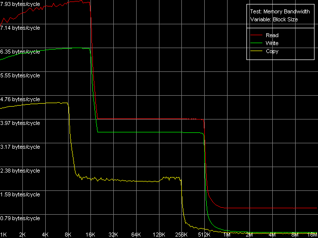 Pentium III-M 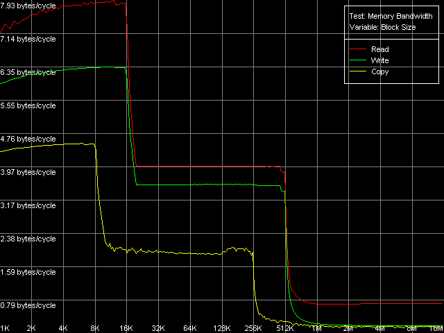 Pentium III-S 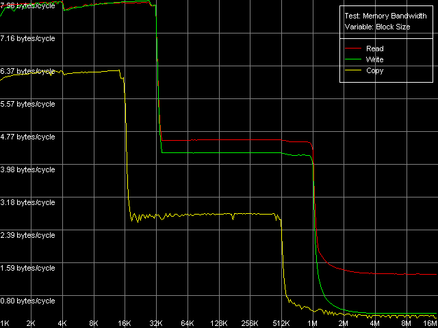 Pentium M Note that only the third platform supports the SSE2 extensions. The test results of Pentium M with this instruction set are identical to the results obtained with the SSE extensions. A similar picture was shown by the Intel Pentium 4 platforms. The curves of all the processors look obvious. They indicate that the
CPUs have two-level data caches with the inclusive architecture because
of the bends which correspond to L1 and L2 cache sizes. Pentium III-M and
Pentium III-S have 16KB and 512KB caches, and Pentium M has doubled ones.
But the cache line size of the latter is also doubled and makes 64 bytes
against 32 bytes of the Pentium III family. That is why we can consider
that the cache set sizes (i.e. the number of lines) of the Pentium M remains
the same, only the line size changes.
Now let's estimate the speeds of the d-cache levels. First of all we will compare the Pentium III-M and Pentium III-S. We can see that the real bandwidth of the L1 and L2 d-caches at reading is equal when the MMX and SSE registers are used. The L1 efficiency makes 7.93 bytes/clock and it's lower at writing (6.36 bytes/clock, MMX registers; 6.58 bytes/clock, SSE registers), which indicates that only one 64-bit value is transferred (a whole MMX register or a half of SSE) at one L1 access. The L2 cache has a lower bandwidth which doesn't depend on the register type used - 4.00 bytes/clock at reading and 3.55 bytes/clock at writing (i.e. at one access to this cache level only one 32-bit value is transferred during total reading/writing). So, the mobile and server versions of the Pentium III have the same speed parameters of the data cache. Let's see how they perform at reading/writing at the RAM level. The mobile platform falls behind the server one (739.4MB/s against 994.4MB/s at reading, 157.2MB/s against 273.6MB/s at writing). But it can depend on the chipset types used, not the processors as they do not differ when accessing the data caches. In both cases the RAM bandwidth at writing is very low - 14.7% (Pentium III-M) and 25.6% (Pentium III-S) of the theoretical maximum equal to 1066MB/s. Let's see what d-cache/RAM bandwidth the Pentium M has. The L1 efficiency in reading remains almost the same (7.94-7.98 bytes/clock against 7.93), and significantly grows at writing, mostly with the MMX registers (7.96 bytes/clock against 6.36, 25% difference) than with the SSE (7.52 bytes/clock against 6.58, i.e. the growth makes 14%). The L2 cache efficiency grows up as well, and it looks the same for the MMX and SSE registers. The speed gain, compared to the Pentium III, in case of L2 reading makes 14%, and in case of L2 writing it makes 20%. We can't compare the absolute memory bandwidth values because of different memory types used. But we can compare the relative values of the real RAM BW. The effective DDR reading on Pentium M makes 81.6% of the theoretical maximum (2133MB/s), which is comparable to the Pentium III (69.3% on Pentium III-M and 93.2% on Pentium III-S). The efficiency at writing is much lower here - 22.6%, which is similar to the data obtained on Pentium III (14.7% and 25.6% on the mobile and server versions). Maximum RAM BandwidthWe'll try to get the most from the memory subsystem, i.e. the maximum real memory bandwidth using different optimizations. The following methods are used in case of reading:
The values are calculated relative to the maximum RAM BW of the memory
types used (1066MB/s, PC-133 SDRAM; 2133MB/s, PC2100 DDR) so that we can
compare the results.
* the parentheses contain the values calculated relative to the theoretical maximum bandwidth of a given memory typeAll the processors equally win when reading data from RAM using the Software Prefetch: 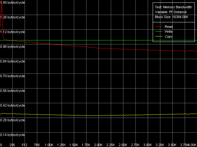 Pentium III-M  Pentium III-S 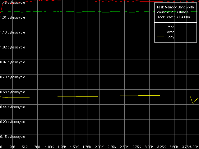 Pentium M It's interesting that in the Pentium III CPUs the real RAM BW rapidly grows up in case of the minimal prefetch length (32 bytes, especially on Pentium III-M), and when it increases the Software Prefetch becomes less efficient. At the same time, in the Pentium M the Software Prefetch efficiency hardly changes starting from the minimal prefetch length (64 bytes) up to the memory page edge (4096 bytes). The Software Prefetch at reading on the Pentium III CPUs allows for 96% of the maximum theoretical RAM BW, while the Pentium M reaches only 88% of the maximum RAM BW. Also remember that the values reached with this method are maximal for the Pentium M. The Block Prefetch methods, especially the first one, show that they are not applicable to Intel's processors. Only the Pentium III-M get a certain gain, while the other CPUs have the RAM BW either lower than the average one (Block Prefetch 1, Pentium III-S and Pentium M) or equal to them (Block Prefetch 2, Pentium III-S and Pentium M). Finally, the cache lines reading methods demonstrate the difference between the processors. On the Pentium III-M the scores are almost equal to the average real RAM BW, on the Pentium M the real RAM BW is a bit greater (up to 84% of the theoretical maximum), and the Pentium III-S scores the best results! (up to 98.5% of the maximum bandwidth). That is why there's some difference between the mobile Pentium III-M and server Pentium III-S not only on the level of the chipsets but also on the CPU level. Now we are going to look at the maximum real RAM BW at writing especially
because its average scores are far not optimal. Non-Temporal Store method,
Memory
Bandwidth test, any of Maximal RAM Bandwidth presets and the
cache lines writing method (D-Cache Bandwidth test, L2 Cache-RAM
Bus Bandwidth preset).
* the parentheses contain the values calculated relative to the theoretical maximum RAM bandwidthThe Non-Temporal Store method ensures a good speed growth on all the platforms, especially on the Pentium III-M (4.7 times), but in the absolute scores the leaders are Pentium III-S (79.7%) and Pentium M (81.9%). At the same time, the cache line writing method doesn't increases the real RAM BW compared to the average values on any processor. D-Cache/RAM LatencyD-Cache Latency test, D-Cache/RAM Latency preset. 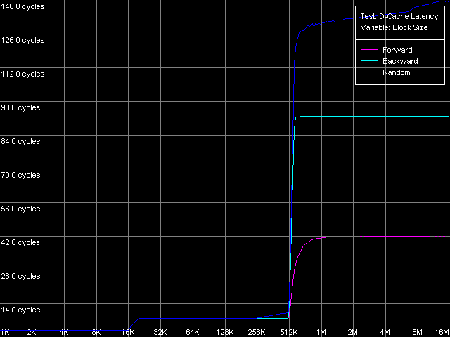 Pentium III-M 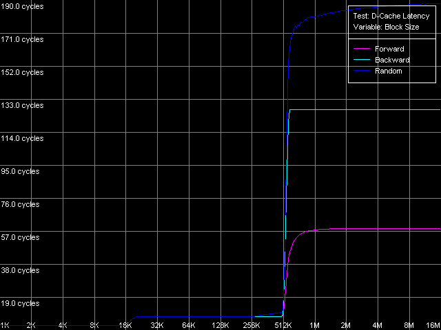 Pentium III-S 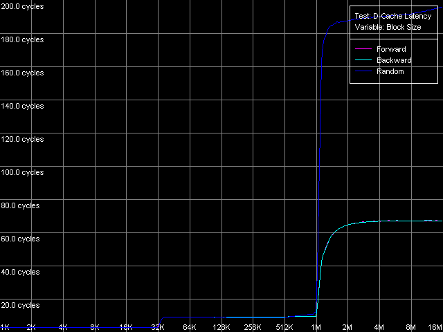 Pentium M The latency curves also have clear bends at the points that correspond to the
L1/L2 d-cache sizes. In all cases the random-access latency curves
gradually increase at the block size of 256 KB and over (Pentium III-M/S)
and 512 KB and over (Pentium M). As we mentioned last
time, it takes place because the D-TLB resources are exhausted.
By the way, judging by this test, the D-TLB size of the Pentium M
as well as its d-cache size, is doubled compared to the Pentium III-M/S
processors. Nevertheless, the D-TLB will be separately studied below.
Now we are going to estimate the average latency of the d-cache levels
and RAM.
* 4 MB block sizeThe L1 cache latency makes 3 clocks for all processors in all access modes. The L2 latency makes 8 clocks in all cases on the Pentium III, but the Pentium M has it equal to 9.5 clocks. The forward access on the Pentium III demonstrates the lowest scores (57.5 ns on the Pentium III-M, 42.0 ns on the Pentium III-S), and the backward access makes the latency twice higher (125.8 ns, Pentium III-M; 91.2 ns, Pentium III-S). Finally, the highest latency is reached in case of the random access to the 4MB chain (183.5 ns, Pentium III-M; 133.5 ns, Pentium III-S). In all access modes the memory latency on the Pentium III-S is approximately 1.37 times lower than on the Pentium III-M. The Pentium M has the improved data prefetch logic algorithm which now works both in forward and backward accesses. The memory latency in this case makes 51.2 ns, between Pentium III-M and Pentium III-S. The random latency on this platform makes 146.7 ns, again between the mobile and server Pentium III platforms. Minimal L2 D-Cache/RAM LatencyIn this test we will gradually increase the number of NOPs inserted between the L2 accesses to see what happens to the L2 latency. D-Cache Latency test, Minimal L2 Cache Latency, Method 1. 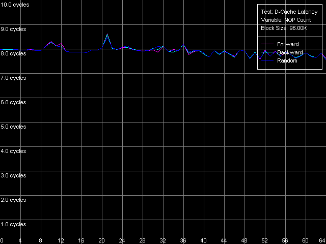 Pentium III-M 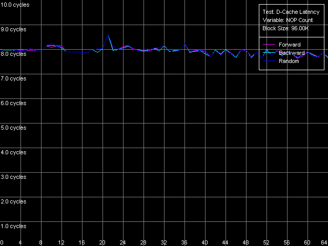 Pentium III-S 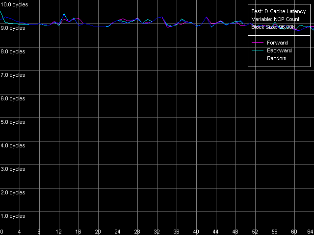 Pentium M On the Pentium III-M/S the L2 latency remains equal to 8 clocks in all access modes. On the Pentium M, even one NOP (execution of which takes one clock) allows reaching the minimal L2 latency equal to 9 clocks. We also tested the L2 latency with another method - Minimal L2 Cache Latency, Method 2. The results look suprising - the L2 latency in all cases is one clock lower compared to the Method 1 (7 clocks for Pentium III-M/S, 8 clocks for Pentium M). Minimal RAM Latency, 4MB Block. 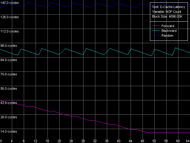 Pentium III-M 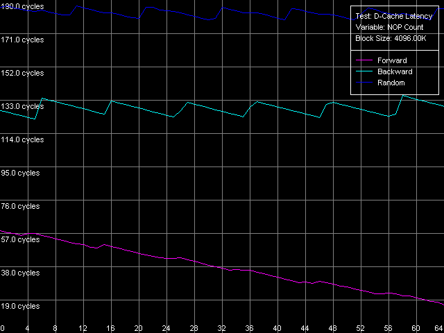 Pentium III-S 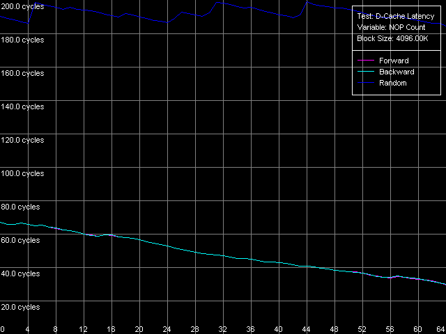 Pentium M The forward curves look different for the Pentium III-M and Pentium III-S, and it might be explained both by the difference in the chipsets and different Hardware Prefetch implementation. The minimal RAM latency in this access mode on the Pentium III-M is reached at 50 NOPs and makes 10.2 clocks (14.0 ns). At the same time, the minimum on the Pentium III-S is reached when the number of NOPs is over 64, and the minimal value reached is 16.5 clocks (11.8 ns, which is lower compared to the Pentium III-M). The backward and random access modes demonstrate the jagged curves, like for the K7/K8 platforms, with the step equal to the CPU/FSB clock factor. The minimal RAM latency in the backward access mode makes 117.0 ns on the Pentium III-M and 87.8 ns on the Pentium III-S. The minimal random latency is again higher - 181.0 ns and 128.2 ns on the mobile and server Pentium III platforms respectively. The dependence of the RAM latency on the number of NOPs on the Pentium
M is similar to the Opteron platform (see benchmarking of the K7/K8).
But the minimal forward/backward latency is not reached even at 64
NOPs, and the minimal value reached is 30 clocks (23.1 ns). The random
latency curves looks jagged again, and we can say that this platform
accesses the memory at every clock of the 100MHz quad-pumped FSB.
The minimal random latency is equal to 142.5 ns. Like the average
random latency, it is lower than that of the Pentium III-M but higher
than that of the Pentium III-S. The higher average and minimal random
latency on the Pentium M vs Pentium III-S can be explained by the
asynchronous memory mode on the former against the synchronous one
of the latter.
* the parentheses contain the values obtained using Method 2 D-Cache AssociativityD-Cache Latency test, D-Cache Associativity preset. 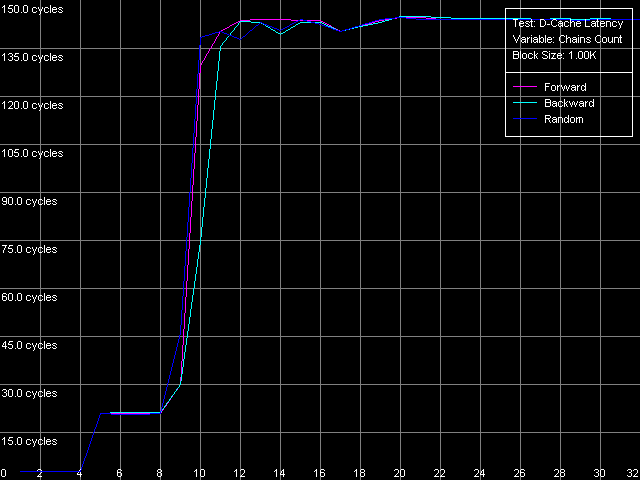 Pentium III-M  Pentium III-S 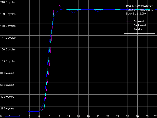 Pentium M The associativity pics (i.e. the cache access latency dependence on the number of dependent access chains) look very clear. In this respect the Intel Pentium III doesn't fall much behind the AMD K7/K8, unlike the Intel Pentium 4. All three processors have three clear zones. In the first one (up to 4 chains inclusive) the cache access latency is 3 clocks in all access modes (L1 latency), which means that the L1 of these processors have the associative level equal to 4. The second zone - 5 to 8 chains inclusive, demonstrates the latency equal to 20 clocks (Pentium III-M/S) and 11 clocks (Pentium M). It corresponds to the L2 latency the associative level of which equals 8, as specified. You can see that on the Pentium III platform the L2 latency in these tough test conditions is 2.5 times higher, like on the K7/K8 platforms. It's caused by the overheads for reassociation of the cache lines with the memory lines. At the same time, the multi-segment access on the Pentium M causes the minimal latency growth (from 9.5 to 11 clocks), which means that the algorithm of the set-associative data cache was much improved (which traditionally follows the LRU principle). Finally, the third zone, from 9 to 32 access chains inclusive, correspond to the maximum RAM latency in all access modes (Hardware Prefetch is not used in the forward/backward access modes here!). Real L1-L2 Bus BandwidthIntel says that the Pentium M features the Advanced Data Transfer Cache. Let's see if there's really any difference in realization of the L1-L2 d-cache bus between these processors. D-Cache Bandwidth test, L1-L2 Cache Bus Bandwidth preset.  Pentium III-M 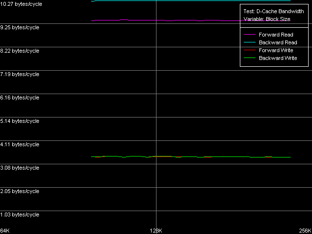 Pentium III-S 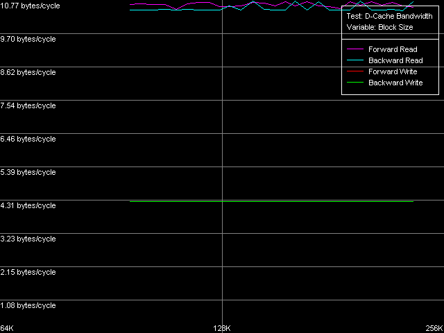 Pentium M All the processors have a 128-bit data bus between two cache levels,
and the maximal real values reached are far from the theoretical limit
equal to 16.0 bytes/clock.
The qualitative estimation of the real L1-L2 bandwidth shows that it's equally effective of the Pentium III-M and Pentium III-S. These processors reach the maximum real L1-L2 BW in the backward read access mode - 10.27 bytes/clock (64.2% of the theoretical maximum). At the same time, its write efficiency is much lower, which is typical of the inclusive d-cache architecture - 3.44 bytes/clock (21.5% of the theoretical maximum). Pentium M has a certain gain (the read efficiency increased up to 67.3%, the write one up to 26.7%), but the gap is so inconsiderable that we can't call the d-cache of this CPU "Advanced Data Transfer Cache". Just compare to the L1-L2 bus of the Pentium 4 Northwood/Gallatin which reaches almost 100% efficiency of utilization of the 256-bit L2-L1 bus. By the way, the fact that the d-cache bus of the Pentium M is 128-bit and the real cache line size is doubled doesn't add any benefit to this processor. 64 bytes take 4 clocks even at the maximum speed of 16 bytes/clock. At the same time the L1 latency remains equal to 3 clocks, that is why the line requested will be available with the latency of at least one clock. Let's check it using the D-Cache Arrival test. Let's look at the summary latency of two accesses to the same cache line as the distance between these accesses increases from 4 to 60 bytes. L1-L2 Cache Bus Data Arrival Test 1, 64 bytes. 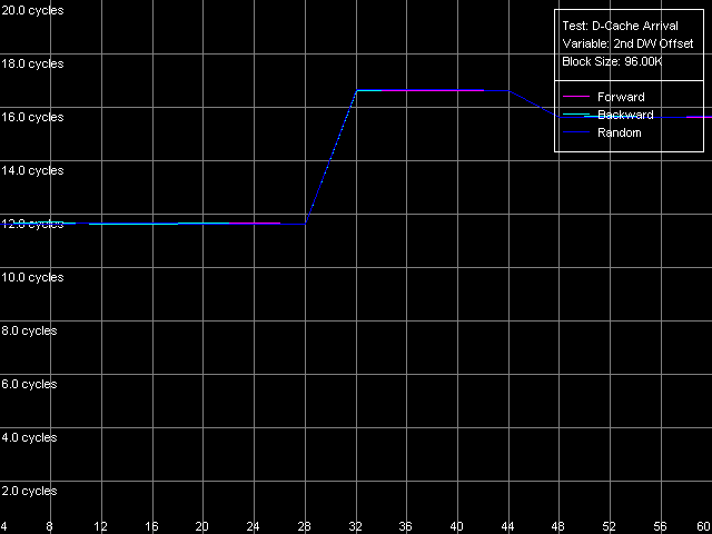 Pentium M The latency of two accesses remains minimal (12 = 3 + 9 clock) up to 28 bytes, and then it grows up by 5 clocks. Why it decreases by 1 clock after 48 bytes is not clear yet. Nevertheless, it means that the 64-byte line requested is not immediately available for the L1 cache. It's not clear how data travels from L2 to L1, but arrival of the number of bytes less than 32 at 3 clocks corresponds to the real L1-L2 bus bandwidth of this processor measured above. Let's see which position of the line reads first from L2 to L1? (in case of the AMD K7/K8 processors the line could be read from any position divisible by 8 bytes). L1-L2 Cache Bus Data Arrival Test 2, 64 bytes. 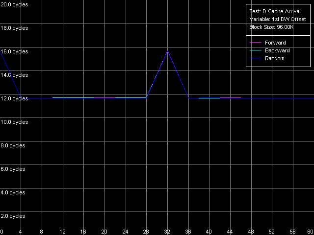 Pentium M This test reads the second element of the cache line with the offset equal to 60 bytes relative to the first element's offset which is variable. So, the initial point (0 bytes) corresponds to the real request of the second element with the 60-byte offset while the following ones correspond to the second element's request shifted from the first one by 4 bytes to the left. The latency increases from 12 to 16 clocks, and it means that the request of the last element of the cache line is connected with latencies indeed. The second maximum takes place when the second element offset is 32 bytes, and it means that the request of the (32 - 4) = 28th bytes is caused by the same latency. So, the test shows that reading of the cache line can start not only from the 0 element but also from the middle (i.e. at the offset of 32 bytes). In the first case the line reads in the following sequence: 0-31, 32-63, in the second case: 32-63, 0-31. That is why in the first case the latency takes place when the 60th element is read, in the second case - when the 28th one is read, which are the last line elements requested. Trace Cache, decode efficiencyLet's estimate key parameters of the I-cache, decoder and execution resources of the processors. I-Cache test, L1i Size / Decode Bandwidth, CMP Instructions 3 preset (the code consists of a series of 6-byte instructions - cmp eax, 0x00000000).  Pentium III-M 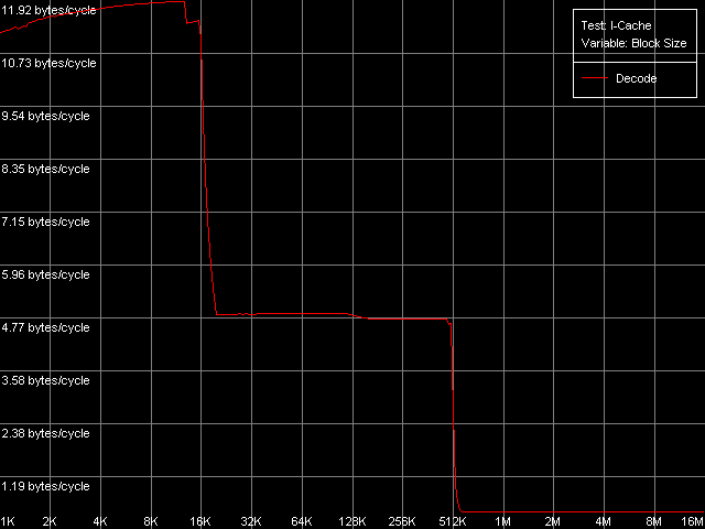 Pentium III-S 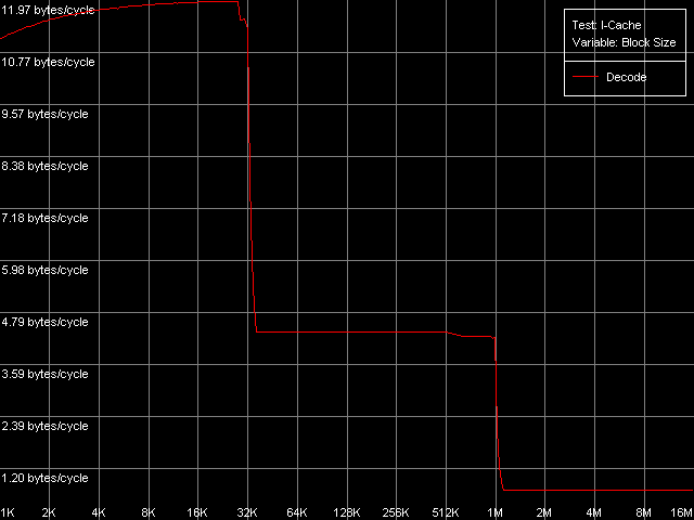 Pentium M The L1 i-cache size of the Pentium M doubles compared to the L1i of Pentium III and makes 32 KB. The 16 - 256KB zone on the Pentium III and 32-512KB zone on the Pentium M corresponds to the L2 cache which is a uniform data/instruction cache for all processors, including AMD K7/K8 and Intel Pentium 4. Obviously, the inclusive cache architecture covers the code caching as well. By the way, exactly in this zone you can notice that the code execution speed drops if the code block exceeds 128 KB (Pentium III-M/S) or 512 KB (Pentium M). It's similar to the Intel Pentium 4 platforms and we explained it by exhaust of the I-TLB resources. Here we can say that the I-TLB of the Pentium III-M/S contains only 32 entries (128KB/4KB), while the Pentium M has a 4 times larger one (up to 128 page descriptors, 512KB/4KB). Let's return to the L1i/L2 efficiency. For this purpose we will estimate
data obtained in other subtests of the I-Cache test.
First comes decoding of small code blocks which fit the L1i cache. The maximum decode/execution rate makes 2 instructions/clock for all three CPUs, and it's reached only in case of the simplest instructions like NOP, TEST, CMP 1, CMP 2 and CMP 3-6. By the way, the rate of execution of the last ones doesn't depend on the 'immediate' field size (0, 8, 16 or 32 bits), like in AMD K7/K8, but not in Intel Pentium 4. Well, the Pentium III decoder is much closer to the K7/K8, than to the completely different Pentium 4. The rate of execution of these instructions on the Pentium M is just a little bit higher, that is why there are hardly any considerable changes in the CPU microarchitecture on the level of the decoder and execution units. Far not all independent instructions are executed on these processors at the most possible speed. The independent instructions like SUB, XOR and XOR/ADD have the execution rate of one instruction per clock. It looks like the processor can't solve such dependencies. I wish the Pentium M had any advancements here. Let's prove it with the facts from Intel's documentation.
The dependent instructions take one CPU clock (per one instruction) on all three processors in any ALUs. CMP instructions are a special case. They contain two "useless" prefixes, REP and Address Override (Prefixed CMP 1-4). They are executed very slowly, especially on the Pentium M (one instruction needs 4 CPU clocks!), that is why the Pentium III/Pentium M do not shine in prefix clipping. Let's test it. Prefixed NOP Decode Efficiency Test.  Pentium III-M 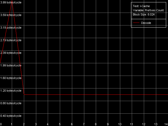 Pentium III-S  Pentium M Instructions with prefixes can be efficiently executed if there's only one prefix, if there are more, the performance drops down. The Pentium M doesn't shine in this test at all. But the Pentium M provides a higher rate of instruction decode/execution from the uniform L2 cache. In most cases (both dependent and independent instructions) the speed grows up by 18%, and even by 34% for TEST and CMP 1 instructions. But execution of the CMP 2 and CMP 3-6 look worse: the speed of their execution from L2 falls down by 15 and 10%, respectively. The efficiency of execution of the Prefixed CMP from L2 also falls down by 16%. Instruction cache associativityTo measure the associative level of the L1i/L2 cache we have I-Cache Associativity test which deals with the simplest NOPs which are located not in one large unit but have different memory addresses with "bad" offsets for the CPU cache.  Pentium III-M 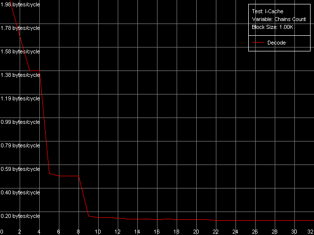 Pentium III-S 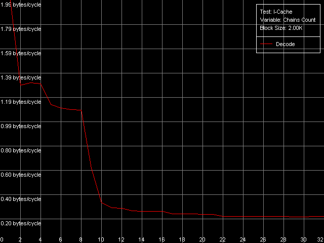 Pentium M The curves of the Pentium III-M and Pentium III-S look identical, but the one of the Pentium M is different mainly because the speed of execution from L2 (5-8 zone) is much higher on this processor. But the general picture is clear: the L1i associativity is 4, and the uniform L2 cache has it equal to 8 (the same value is achieved in the d-cache associativity test). D-TLB parametersThe final tests deal with the buffers of translation of virtual memory page addresses into physical addresses (D-TLB/I-TLB). First of all, we will measure the TLB size using the D-TLB test. D-TLB Size. 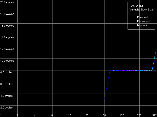 Pentium III-M 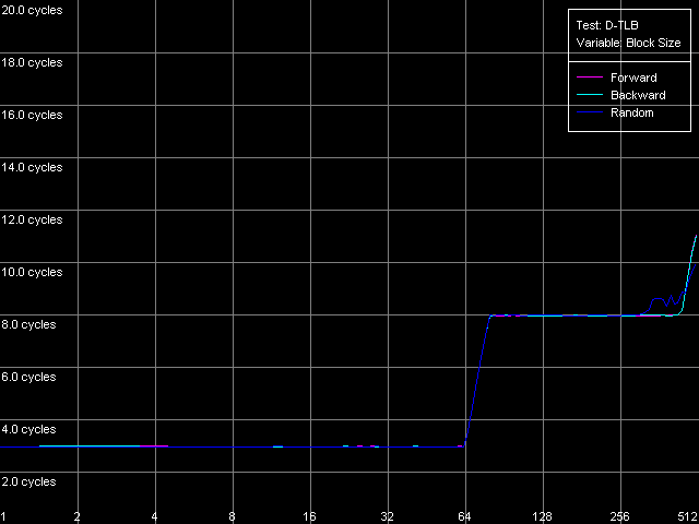 Pentium III-S 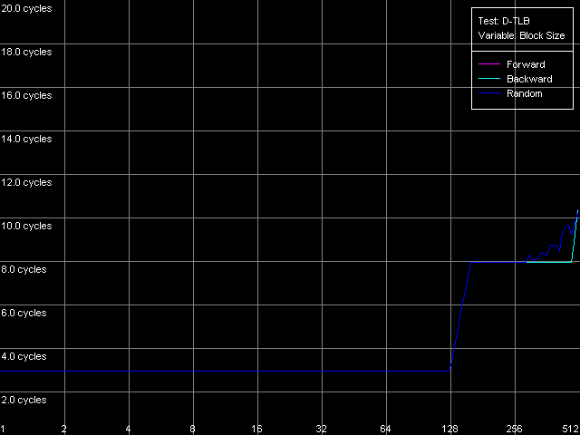 Pentium M The assumption about the D-TLB size made in the first section is proved: in case of the Pentium III-M/S it can't contain more than 64 entries, and in the Pentium M it's extended to 128 entries indeed. The D-TLB architecture is traditional for Intel's processor - it consists of 1 level. Finally, the D-TLB miss easily tells upon the L1 latency - it increases up to 8 clocks in all processors, like in AMD K7/K8, and not that tremendously, like in Intel Pentium 4. Now we are going to measure associativity of the only D-TLB level. D-TLB Associativity, 32 Entries - exactly such number can fit the D-TLB of each of the processors. 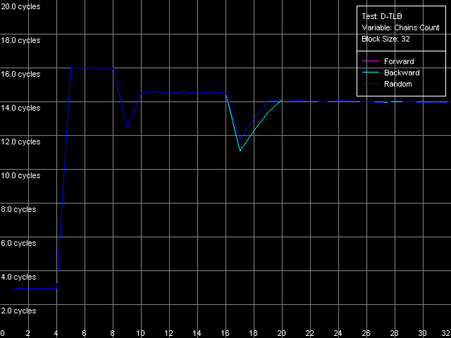 Pentium III-M  Pentium III-S 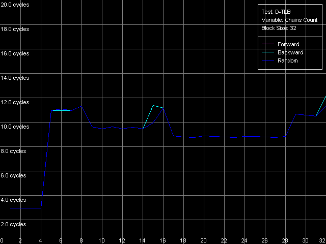 Pentium M The curves of the Pentium III-M and Pentium III-S look identical again. The D-TLB associativity equals 4, and its "drop" pushes up the L1 latency up to 14 clocks on average. The Pentium M looks much better: its D-TLB associativity is also 4 but the average latency when it's exhausted falls down to 9 clocks. I-TLB parametersFirst we will measure the I-TLB Size. 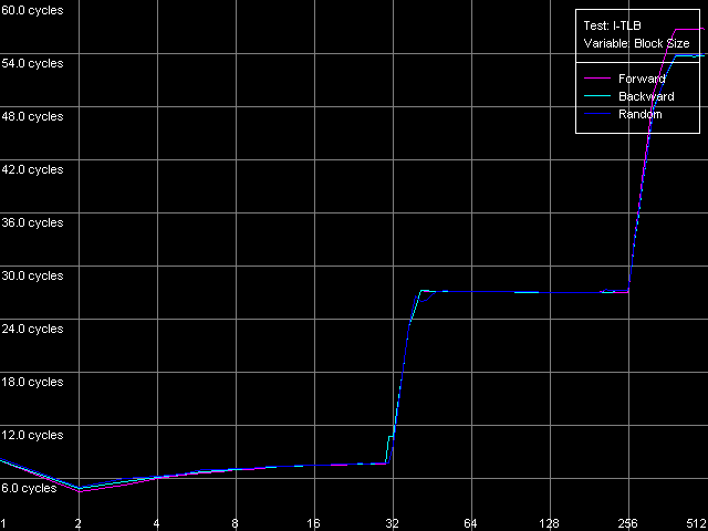 Pentium III-M  Pentium III-S  Pentium M The assumption we made before is true - the I-TLB of the Pentium M is four times greater (128 entries) as compared to the Pentium III-M/S. The I-TLB miss stronger affects the latency of execution of the series of unconditional jumps (it grows up to 27-28 clocks) than the effect of the D-TLB miss on the L1d latency. The jump at the 256-page mark on the Pentium III-M/S curves is caused by the exhausted L1i of these processors and by the L2 i/d cache zone hit. Now we are to estimate the I-TLB associativity for today's processors. I-TLB Associativity, 16 Entries for the Pentium III-M/S with a relatively small buffer, and I-TLB Associativity, 32 Entries for the Pentium M.  Pentium III-M  Pentium III-S  Pentium M The I-TLB associativity is 4 for all CPUs, and if it's exceeded the latency of execution of the "jumps" increases (27 clocks) like in the case when the I-TLB is exceeded. ConclusionTo make a conclusion on the the new generation of the Pentium III family and a key component of the Intel Centrino Mobile Technology - Intel Pentium M - we will compare two Intel specified parameters to what we obtained in the low-level tests of Intel Pentium III CPUs' parameters. The first distinguishing feature, by Intel, is the doubled instruction and data cache sizes. It's almost true because the cache line also doubled, that is why the cache size remains the same regarding the number of lines. The D-TLB and I-TLB are definitely greater, and it's really beneficial for the Pentium M. One more advantage is the improved latency of the data cache and TLB when their associativity is exhausted. On the other hand, the L2 latency got higher (by one clock) because the L1/L2 bus bandwidth is still 128-bit, and additional latencies are needed to transfer a whole 64-byte cache line. Intel's second announcement is the microarchitectural changes in the
CPU core. Frankly speaking, we tested the decoder and execution units but
didn't reveal any noticeable changes on this level. The maximum code execution
speed remains the same, and this processor doesn't solve dependencies or
clip prefixes better than the Pentium III. On the other hand, instruction
reading from the L2 cache works faster now. But this is not that urgent
as there are hardly any programs that need to execute a continuous 512KB
code block.
Dmitry Besedin (dmitri_b@ixbt.com)
Write a comment below. No registration needed!
|
Platform · Video · Multimedia · Mobile · Other || About us & Privacy policy · Twitter · Facebook Copyright © Byrds Research & Publishing, Ltd., 1997–2011. All rights reserved. | |||||||||||||||||||||||||||||||||||||||||||||||||||||||||||||||||||||||||||||||||||||||||||||||||||||||||||||||||||||||||||||||||||||||||||||||||||||||||||||||||||||||||||||||||||||||||||||||||||||||||||||||||||||||||||||||||||||||||||||||||||||||||||||||||||||||


