 |
||
|
||
| ||
|
||
|
||
| ||
In the last review devoted to our RightMark Memory Analyzer Benchmark we studied the key features and principles of testing of the most important platform parameters (CPU/chipset/memory subsystems). Now we are going to find out whether the principles of objective measuring of low-level parameters of today's platforms are applicable. We start the series of the platform measurement reviews with AMD K7 (Athlon XP CPU, Palomino core) and K8 (Opteron 244 CPU). Testbed and software
Real D-Cache/RAM BandwidthTo estimate the real average bandwidth of the data cache and RAM and data cache levels size we will use the first RMMA test (Memory Bandwidth) and D-Cache/RAM Bandwidth, MMX Registers preset. 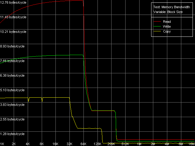 AMD Athlon XP 1800+ 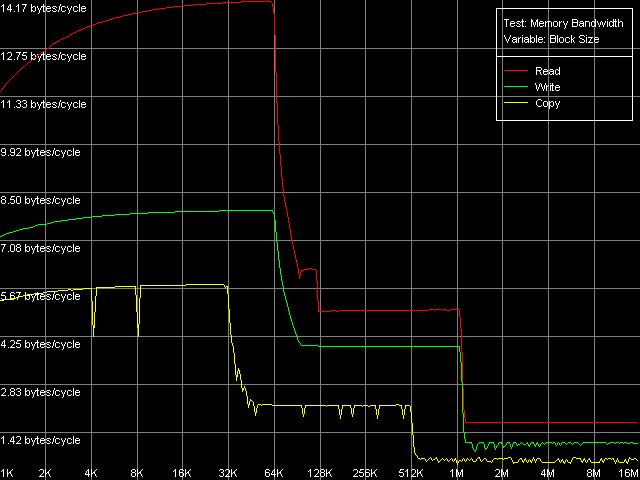 AMD Opteron 244 Both processors have the L1 cache equal to 64 KB (the first bend on the Read and Write curves). They also have a bend at the point that equals the summary size of the L1+L2 caches (320 KB and 1088 KB respectively). This is a typical sign of the exclusive data cache architecture (and it is such in AMD K7/K8 CPUs), while the curves in case of the inclusive architecture have bends at the points that correspond to L1 and L2 (and L3) cache sizes. The average bandwidth of the L1 cache, or rather L1-LSU tandem, in reading operations (12.8 bytes/clock, K7 and 14.2 bytes/clock, K8) is a bit lower than the theoretical maximum of 16 bytes/clock which corresponds to the 128-bit data bus between L1 and LSU (Load-Store Unit) specified in AMD's documentation (two 64-bit ports). The L1 efficiency in writing is twice as low, which means that only one port in used for writing operations. In case of K7 the average memory bandwidth (real MB) was 900 MB/s in reading and 690 MB/s in writing. For K8 it makes 3100 MB/s and 2025 MB/s. In both cases it's much lower than the maximum theoretical memory bandwidth. But it was expected because this test doesn't use any optimizations aimed at reaching the maximum possible memory bandwidth. We will try to reach them in the next tests, and now we are going to carry out the same tests using SSE instead of MMX (D-Cache/RAM Bandwidth, SSE Registers preset). 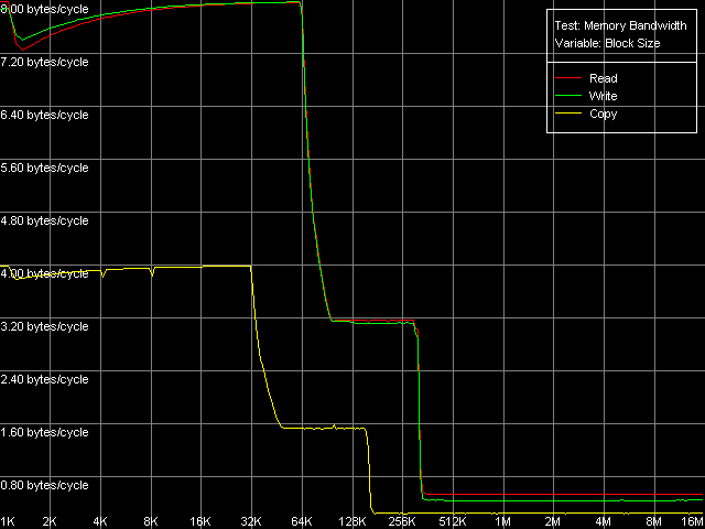 AMD Athlon XP 1800+ 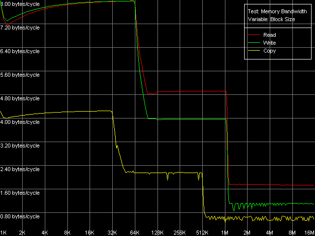 AMD Opteron 244 The results are expected for K7 and unexpected for K8. No wonder that AMD K7 CPUs work less efficiently with the SSE registers than their competitors. Some suggested that Athlon XP/MP doesn't have a dedicated SSE unit and its functionality is emulated by 3DNow! The utmost real L1-LSU memory bandwidth makes 8 bytes for 128-bit values (64 bits/clock), i.e. it takes one clock to transfer half of the operands stored in the XMM register in spite of the 128-bit capacity of the respective bus. However, I'm surprised that AMD hasn't changed anything in the K8 architecture (yet since K7), i.e. the engineers didn't take care to improve transfer of 128-bit data on L1-LSU bus. Its efficiency in writing is the same (8 bytes/clock, which is the same for the MMX registers as well). Maximum RAM BandwidthTo estimate the maximum real RAM bandwidth in read/write operations we will use the MMX registers as they produced the best results in both cases. First of all we are going to apply the Software Prefetch method in reading with the direct memory writing enabled (Non-Temporal store). Preset: Maximal RAM Bandwidth, Software Prefetch, MMX Registers. 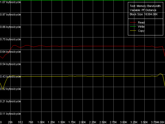 AMD Athlon XP 1800+ 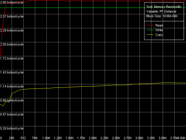 AMD Opteron 244 The difference between the K7/K8 architectures is significant. The Software Prefetch for K7 is pretty weak. The maximum memory bandwidth in reading makes 1047 MB/s (the prefetch length is 320 bytes and over), which is just 1.16 times over the average value. At the same time, the benefit from the Software Prefetch on K8 is considerable: the real memory bandwidth in reading reaches 5150 MB/s (the prefetch is 640 bytes and over), which is 1.66 times as great as the ordinary data read rate. AMD is really praiseworthy for such a good implementation of the Software Prefetch. Let's see how the Non-Temporal store mode tells on the real memory bandwidth at writing. It makes 1647 MB/s for the Athlon XP (2.38 times greater than the average one) and 4880 MB/s for Opteron (2.41 times greater). The benefit is quite great and comparable for both platforms. Moreover, the real memory bandwidth obtained in this benchmark is maximum and can't be reached using other methods (as you will see later). So, since the real RAM bandwidth at reading on the first testbed (Athlon XP) didn't reach its maximum let's try to get it using other methods. At the same time we will check them for our second platform (Opteron). Block Prefetch 1 Method is recommended by AMD for reaching the maximum real bandwidth at reading on K7 systems (preset: Maximal RAM Bandwidth, Block Prefetch 1, MMX Registers). 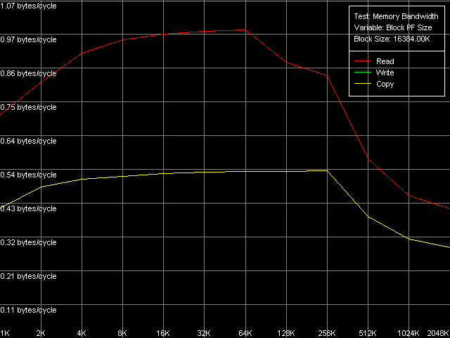 AMD Athlon XP 1800+ 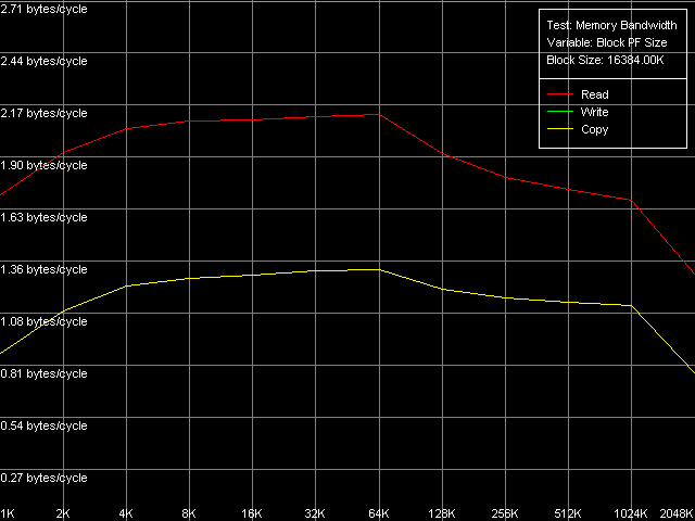 AMD Opteron 244 Since the Software Prefetch / Block Prefetch methods deal with data reading only, the real bandwidth on both platforms doesn't change. However, we reached the maximum real RAM bandwidth for K7 in reading which equals 1505 MB/s (1.67 times greater compared to the average real memory bandwidth) at the prefetch block size of 64 KB which matches the L1 cache. As the prefetch block size grows up (the L2 zone is reached) it gets a bit narrower, and then it sharply falls down (when the prefetch block size gets equal to 256 KB on Athlon XP and 1 MB on Opteron). The read curves look more or less similar for both platforms, but the maximum real RAM bandwidth at reading on Opteron is not reached (it makes just 3813 MB/s, i.e. 123% of the average value). At the same time, there's a certain difference between these two AMD platforms. The maximum real bandwidth at copying on Athlon XP is reached when the prefetch block size equals the L2 (256 MB), while on Opteron it looks like the curve in case of reading operations, having two bends at 64 KB (L1) and 1024 KB (L2). It might be because of the different ways of utilization of data caches of these processors in copying operations using Non-Temporal Store method. There's one more data prefetch method (Block Prefetch 2). The difference between both methods was described in our first article). This, second, method is recommended in the guide of 64-bit software optimization for AMD K8 platform for reading/copying of large data blocks (there's no information whether it can be used for 32-bit software too). Let's see whether it matches for the platforms tested (preset: Maximal RAM Bandwidth, Block Prefetch 2, MMX Registers).  AMD Athlon XP 1800+  AMD Opteron 244 This method doesn't suit for Athlon XP though there's some speed gain (957 MB/s against average 900 MB/s, i.e. 1.06 times greater). The scores for Opteron look surprising. The real RAM bandwidth grows up (4366 MB/s vs 3100 MB/s, 1.41 times gain). But the gain is not that weighty compared to the Software Prefetch (1.66 times). It looks like this method is well suited only for the 64-bit code. I don't believe it but I hope that we will soon get a chance to check it. One more method is reading/writing of whole cache lines (the size of which is 64 bytes for our processors) from memory to CPU cache (reading) or from cache to memory (writing) instead of reading/writing of separate 64-bit (or 128-bit) data into the CPU registers. Let's take the third RMMA subtest (D-Cache Bandwidth) and choose L2 Cache-RAM Bus Bandwidth preset.  AMD Athlon XP 1800+  AMD Opteron 244 This time we have finally reached the maximum real RAM bandwidth at reading for Athlon XP (1630-1647 MB/s, which is 1.81-1.83 times greater than the average real RAM BW). By the way, it equals the maximum real RAM BW at writing obtained using Non-Temporal Store method (1647MB/s). This figure can be considered the limit value for this particular system (it depends not only on the CPU type but also on the chipset and memory). Opteron doesn't shine in this test (4490MB/s, 1.45 times over the average), and its results are comparable to the Block Prefetch 2. Writing of whole cache lines looks better than total writing -
the difference between the real RAM BW values is minimal (the real RAM
BW in case of writing cache lines is only 1.04-1.07 times higher compared
to the other method).
So, the maximum real RAM BW at reading/writing for K7 makes 1647MB/s (77% of the theoretical maximum of 2133MB/s). The maximum real RAM BW at reading on Opteron equals 5150MB/s (98% of the theoretical maximum equal to 5250MB/s), and at writing it makes 4880MB/s (93% of the theoretical maximum). D-Cache/RAM LatencyThis test estimates average latency of every D-cache level and RAM. 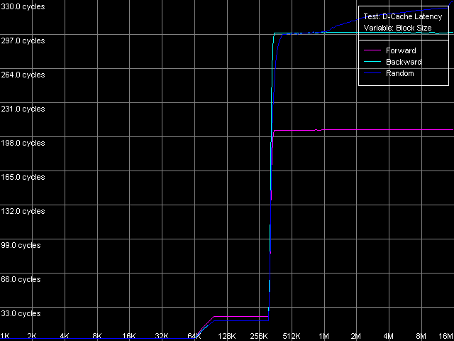 AMD Athlon XP 1800+ 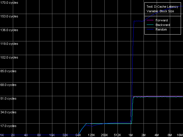 AMD Opteron 244 The L1 cache latency makes 3 clocks for all access methods (forward,
backward, random). At the same time, the L2 cache latency of Athlon XP
is 24 clocks in case of forward access (because of the overheads in the
Hardware Prefetch algorithms realization) and 20 clocks for backward/random
access. The respective values for Opteron are 17 clocks on average (in
all cases). In both cases it's a bit higher than the minimal latency specified.
We will try to reach it in the next test. And now we are going to estimate
the average memory access latency. On K7 it makes about 205 clocks (133
ns) for forward access and about 300 clocks (195 ns) for backward/random
access, which means that the Hardware Prefetch mechanism works well in
case of forward RAM access. Nevertheless, the RAM latency for K8 looks
much better. First of all, the Hardware Prefetch works excellently both
for forward and backward access (the memory latency makes only 50 clocks,
i.e. 28 ns!). The random access latency is a bit higher - 144 clocks (80
ns). The gradual increase of this value in both cases (at the clock size
of 1 MB and over on K7, 2 MB and over on K8) is caused by the growing number
of L2 D-TLB misses, the size of which can provide the effective random
addressing of such data volumes, but not greater.
Minimal L2 D-Cache/RAM LatencyThis test estimates the minimal latency of the L2 cache. 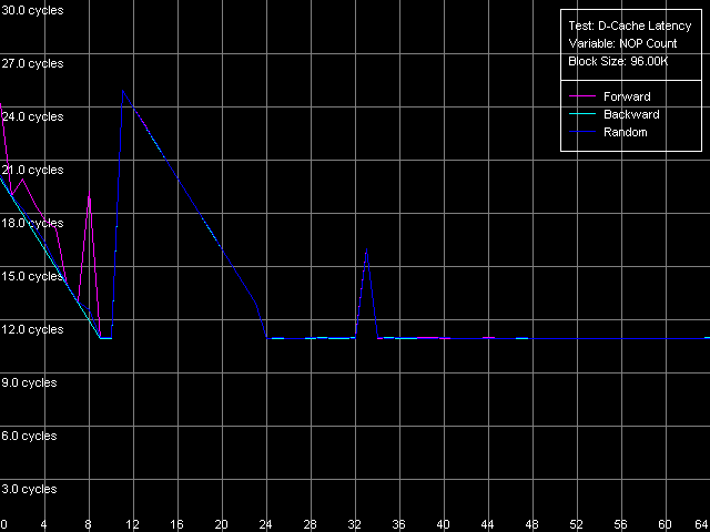 AMD Athlon XP 1800+ 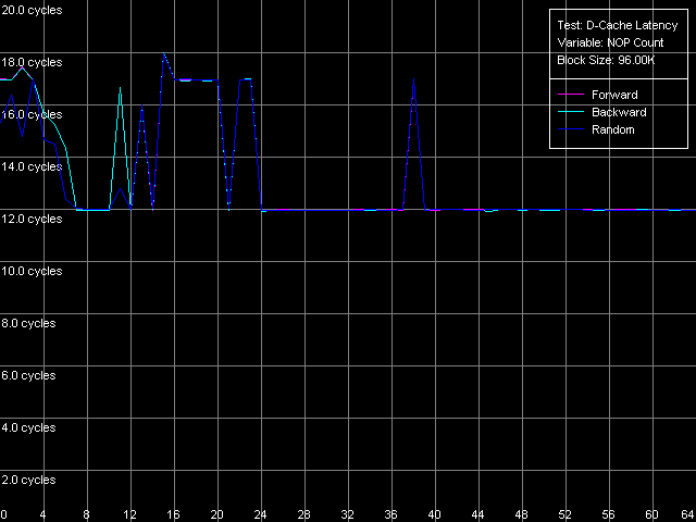 AMD Opteron 244 Note that in both cases the minimal L2 latency (11 clocks, AMD K7; 12 clocks, AMD K8), in all access modes, can be reached in case of 24 NOP. Since it takes exactly one clock to execute every NOP = or eax, edx on AMD K7/K8, it equals the 24-clock L1-L2 bus load between two following accesses. The jumps at the point of 33 NOPs (K7) and 38 (K8) NOPs and the way it gets unloaded before the "24 NOP" mark can't be explained yet. Let's estimate the minimal RAM latency with Minimal RAM Latency, 4M Block preset. Taking into account the latency results obtained above let's reduce the block size to 1MB for K7 and to 2 MB for K8 in order to minimize the losses caused by the L2 TLB misses. 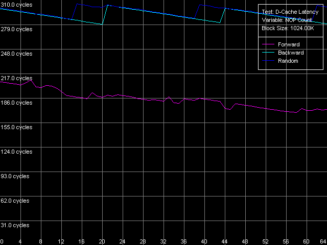 AMD Athlon XP 1800+ 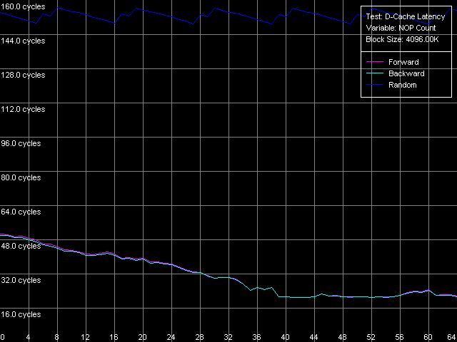 AMD Opteron 244 First comes the K7 platform. The increased L2-RAM bus unload makes the memory forward access latency gradually fall down. This test doesn't show if the minimal value is reached. But the separate test demonstrates that it can be reached in case of 380 NOPs between every two successive accesses and makes 25-26 CPU clocks. At the same time, the backward and random access curves look differently - they have teeth at certain points. The backward access latency is within 280 - 304 clocks (183 - 198 ns), and the random access latency is just a bit higher (284 - 305 clocks, 185 - 199 ns) since we measured it provided that there were almost no L2 TLB misses. The teeth on the backward and random access curves are caused by the fact that a new memory exchange cycle can start/end only at the whole number of FSB clocks. In this case the teeth interval equals 23 NOPs, that is why the memory exchange cycle in this system (with the multiplier equal to 1533.3/133.3 = 11.5) can take place only at every even (or odd) memory bus clock. It's not clear why some AMD K7 platforms behave this way. However, we are sure that it doesn't depend on multiprocessing, as well as on a memory type (DDR or SDRAM), but it must be related to peculiarities of one or another chipset. The minimal RAM latency for Opteron looks different. The minimal latency
for backward/forward memory access latency was reached yet at 39 NOPs (it's
almost 10 times less than the Athlon XP has), and it comes to 21 CPU clocks
(11.7 ns). The random access latency is much higher (probably, this is
the only objective memory latency in systems with Hardware Prefetch enabled).
It varies from 139 to 148 clocks (77 - 82 ns) and has the same tooth-like
curve with the period of 11 NOPs, which means that the memory cycle can
take place at every clock of its 166 MHz bus.
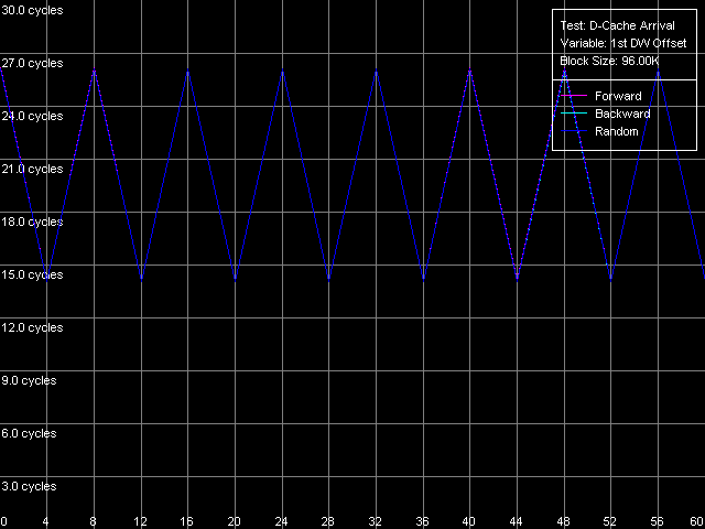
D-Cache Associativity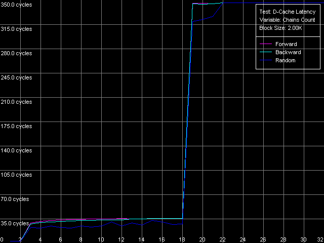 AMD Athlon XP 1800+ 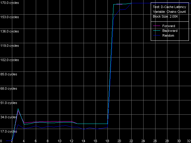 AMD Opteron 244 The curves of AMD Athlon XP and Opteron have areas that correspond to 2-way associative L1 cache (at the number of chains of 1-2), and the latency remains 3 clocks for all access types. The 3-18 area is related to the L2 cache associativity which looks overstated in our case (18 against 16 specified for L2 cache associativity). This directly depends on the exclusive architecture of AMD K7/K8 CPU caches. Since such cache architecture doesn't imply duplicating of L1 data with the help of L2, value 18 equals the "summary" associativity of the L1+L2 D-caches. The processors with the inclusive cache architecture have a different curve, and they bend at the points of associativity of the L1 and L2 caches. Note that the L2 and RAM latency in both cases is overstated at this point, especially in case of the successive access. It happens probably because of the overheads for regular re-association of the cache lines with the memory lines according to the LRU scheme (Least Recently Used) in order to keep in the CPU cache hierarchy all data taken from the "bad" addresses from the standpoint of organization of the CPU D-cache. Real L1-L2 Bus BandwidthIn this case we will use the third test again (D-Cache Bandwidth), with L1-L2 Cache Bus Bandwidth preset. 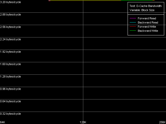 AMD Athlon XP 1800+ 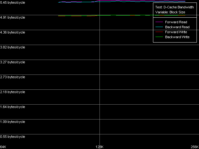 AMD Opteron 244 On Athlon XP the real L1-L2 bus bandwidth was 3.2 bytes/clock for all access types. Note that every access into L2 (one L2 cache line loading into L1) in the exclusive cache architecture is followed by the additional writeback of the excluded line from L1 in L2, i.e. one access transfers a double data size by the L1-L2 bus. In this case the effective L1-L2 bus bandwidth is 6.4 bytes/clock, which corresponds to the 64-bit data bus between L1 and L2 caches. On Opteron the real L1-L2 bus bandwidth is much higher (10.9 bytes/clock with the exclusive architecture taken into account), which corresponds to the 128-bit bus between L1 and L2 caches specified in AMD's documentation. Another interesting peculiarity of the exclusive cache architecture is that the L1-L2 bus efficiency at writing is not worse than that for reading cache lines from L2 into L1. It's especially well seen in the AMD K7 architecture (the real L1-L2 bus bandwidth for reading and writing is 3.2 (6.4) bytes/clock), while in case of AMD K8 the L1-L2 bus efficiency in writing is a bit lower, and the real bus bandwidth makes 4.9 (9.8) bytes/clock. Now we are going to get some more characteristics of the L1-L2 cache with the D-Cache Arrival test which measures the summary latency of two accesses to the same data cache line. L1-L2 Bus Data Arrival, 64 bytes preset. 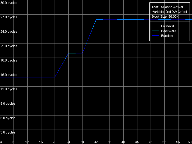 AMD Athlon XP 1800+ 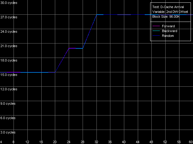 AMD Opteron 244 On the figures above you can see how the summary double-access latency depends on the second access offset (in bytes) relative to the first one. In this case (when the bus is unloaded enough due to the 64 NOPs between two successive accesses to the neighbor cache lines) the forward, backward and random access the lines are degenerate. When the second element of the line is offset within 4-20 bytes relative to the first one the summary latency of two accesses makes 14/15 clocks (for K7/K8), which coincides with the L2 cache access (11/12 clocks) with the following access to the L1 cache (3 clocks). At the same time, the increased summary latency when the offset is 24 bytes and over is caused by the fact that the maximum theoretical bandwidth of the two-way 64-bit L1-L2 bus of the AMD Athlon XP processor at reading makes 8 bytes/clock (during 3 clocks of the L1 access the L2 can transfer as much as 8x3 = 24 bytes). Opteron performs similarly which means that the effective L1-L2 bus capacity in reading operations is 64 bits. This aspect was closely studied in Appendix 1 to the article where we examined the AMD64 architecture. Additional one-clock latency between two successive accesses to the same cache line (by increasing the number of SyncNOPs by one) shifts the diagram border by 8 bytes. If there are more than 5 SyncNOPs this border disappears because 3 (L1) + 5 (SyncNOPs) = 8 L2 cache access clocks is needed to transfer 8x8 = 64 bytes via the L1-L2 bus 8x8 = 64, which is equal to a whole cache line. Finally, let's estimate how cache lines are read from the L2 into the L1 (from its beginning, irrespective of the first element offset, or from a demanded position, turning over the end of the requested string). For this purpose we will draw the diagram that reflects how the summary latency depends on the first word offset relative to the cache line beginning with the following Custom parameters of the D-Cache Arrival Test:
 AMD Athlon XP 1800+ 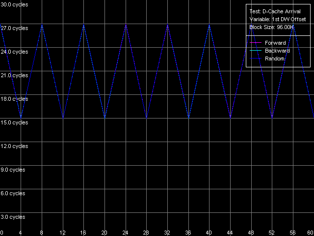 AMD Opteron 244 The usage of the second word offset relative to the first one which is equal to 60 bytes means that the real offset will be -4 bytes (except the first point when the offset is 60 bytes indeed), i.e. the second word will be shifted by one position to the left from the first word, in the cache line. Now look at the diagrams. First of all we must say that the hypothesis saying that data are always read from the beginning of the line irrespective of location of the first element is wrong. In this case, since the second element reading in this test is carried out in the following order: (60, 0, 4, ..., 56), the curves would look identically but would be shifted to the left by 4 bytes. So, in these architectures (K7 and K8) reading of the cache line can start from a non-zero position that depends on where the first element is located. To find out how these values are related to each other let's look at the curves. As you can see, they are based on only two summary latency values - the maximum equal to 26/27 clocks (when the first word offset is a multiple of 8, let's call it even) and the minimum equal to 14/15 clocks (in case of odd offset). It means that in case of the odd first word offsets the data coming from the L2 cache hit the L1 cache immediately while reading of data from the even offsets cause the maximum delay of the second word arrival which is separated from the first word by -4 bytes. The results suggest that the cache line reading from L2 into L1 in AMD K7/K8 processors can start from any offset which is a multiple of 8 bytes. Then reading goes on turning over the end of the requested string - until the whole line is read. Here are two examples. In the first example the data are requested from the "even" offset equal to 24 bytes. In this case data will be read from L2 into L1, at every clock, in the following sequence: (24-31, 32-39, 40-47, 48-55, 56-63, 0-7, 8-15, 16-23). It explains why the second word delay with the actual offset of 24 - 4 = 20 bytes is maximum (26/27 clocks). Now let the first word offset be "odd", for example, 44 bytes. Data will be read in the following order: (40-47, 48-55, 56-63, 0-7, 8-15, 16-23, 24-31, 32-39). It explains why the summary latency at accessing the elements which are offset by 44 and 40 bytes turns out to be minimal (14/15 clocks). This proves the above suggestion. Instruction Cache, Decode EfficiencyFirst of all we will estimate characteristics of the I-Cache levels (remember that the L2 cache can cache both data and an executable code) and effectiveness of decoding of a simple 6-byte instruction cmp eax, 0x00000000, which allows reaching the maximum decoding rate. For this purpose we use the I-Cache test and L1i Size / Decode Bandwidth, CMP Instructions 3 preset. 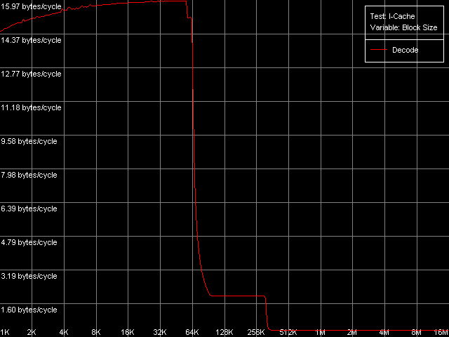 AMD Athlon XP 1800+ 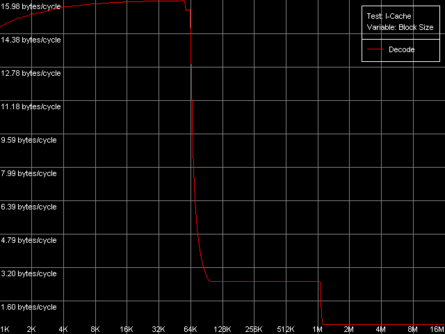 AMD Opteron 244 The instruction L1 cache size (L1i) is as expected equal to 64 KB both
for K7 and for K8. The exclusive L1-L2 hierarchy organization doesn't change
either - it can be also applied to code caching. The decode curves have
the second bend at 320 KB (64+256) on K7 and at 1088 KB (64+1024) on K8.
The efficiency of decoding/execution of the code stored in L1i almost
reaches the maximum value for these architectures of 16 bytes/clock which
was mentioned above when we estimated the real D-Cache L1 bandwidth. Efficiency
of caching of this type of instructions with the L2 cache is much lower.
Let's see how fast other types of instructions from L1i/L2 caches are executed.
We can see that the speed of execution of instructions from the L2 doesn't depend on their type for both K7 (1.97 bytes/clock) and K8 (2.56 bytes/clock). In the second case the efficiency of the L2 code execution is a bit higher (by almost 30%), but both results are still far from the theoretical limit for the 64-bit L1-L2 bus in reading. In case of the L1i cache decoding of large instructions (like 6- and 8-byte cmp) is limited by the L1 bandwidth of 16 bytes/clock (2.66 instructions/clock and lower). In case of small independent instructions (1-, 2-, 4-byte) it's quite possible to reach the maximum decoding/execution rate which equals 3 instructions/clock for K7/K8. The decoder in K8 has some advancements for decoding simple ALU operations which allow reaching the maximum speed of their execution as compared to the decoder in K7. Now we are going to estimate associativity of the L1i and I/D L2 caches (associativity of the latter must equal the one we found before when analyzed the D-cache L1/L2 associativity). I-Cache Associativity preset. 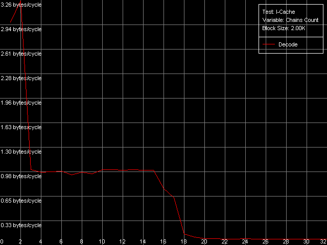 AMD Athlon XP 1800+ 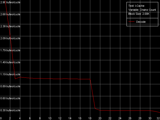 AMD Opteron 244 The test results are pretty clear, especially for Opteron. In both cases the L1i associativity is equal to 2, and the summary L1i+L2 associativity equals 18, which proves that the cache levels in these processors have the exclusive organization. Now let's see how effectively these processors can handle a large amount of (actually useless) prefixes which precede a single sensible x86 instruction. Prefixed NOP Decode Efficiency preset. 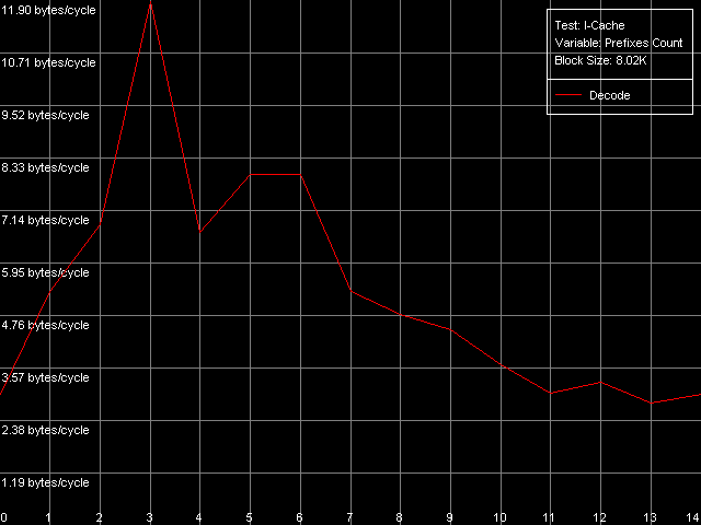 AMD Athlon XP 1800+ 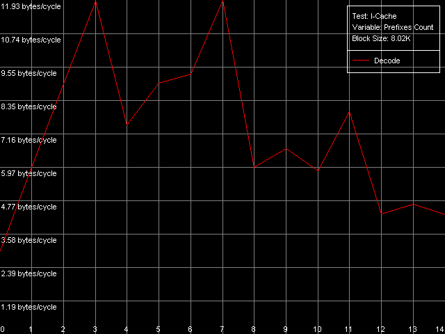 AMD Opteron 244 The curve for K7 reaches the maximum at the number of prefixes equal to 3 (11.2 bytes/clock / 4 = 2.8 operations/clock), and as the number of prefixes grows up the decode efficiency (in quantity of operations) quickly goes down. The K8 handles prefixes a bit better, though not that good as we wanted it to be. The curve got additional maximums but they are not such when recalculated into quantity of executable operations. However, exactly such instructions - [0x66]nNOP - are recommended as a neutral code in AMD's guide for software optimization for K8 processors, for example, for aligning the cycle start border. D-TLB levels characteristicsFirst of all we are going to examine the general picture of TLB levels for each processors. For this purpose we use D-TLB test and D-TLB Size preset for Athlon XP. For the second system (Opteron) we made manual settings having increased the maximum number of D-TLB entries calculated up to 1024, because the L2 D-TLB size of this processor is greater than 512. 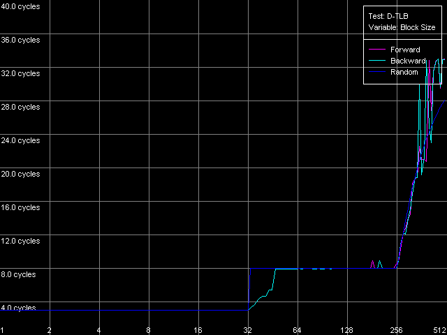 AMD Athlon XP 1800+ 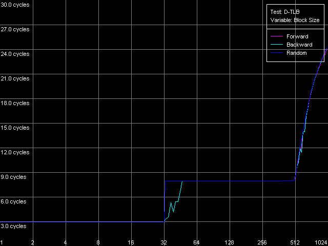 AMD Opteron 244 Both processors have the two-level D-TLB system with the L1 D-TLB size equal to 32 entries. The L2 D-TLB size for XP makes 256 entries and in Opteron it's twice as great (512 entries). Since the second jump lies in the zone that corresponds to L2 D-TLB size, rather than to L1+L2 D-TLB we can suggest that the D-TLB structure of both processors have an inclusive architecture (unfortunately, the TLB levels organization details are usually not reflected in documentation if there are several such levels). In both cases the L1 D-TLB miss lifts up L1 access latency up to 8 clocks. L2 D-TLB misses makes a greater effect - as the number of misses grows up the L1 access latency gradually grows up to the values that definitely exceed the L2 latency. According to AMD's documentation, L1 D-TLB is fully associative for K7/K8. Let's find out if it's true. Preset: D-TLB Associativity, 16 Entries, the entries can easily fit in L1 D-TLB. 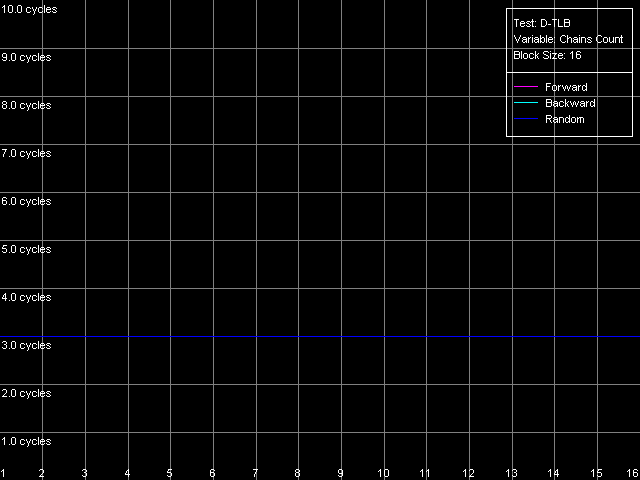 AMD Athlon XP 1800+ 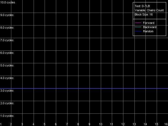 AMD Opteron 244 The test proves that the L1 cache latency equals 3 clocks when accessing 16 memory pages for both processors at any number of dependent access chains. The curves will look the same for the maximum number of chains equal to 32. It means that the L1 TLB is fully associative (because its associative level is not lower than its size). Now we are going to estimate the L2 D-TLB associative level and for this purpose we use the number of pages which is admittedly higher than the number of entries in L1 TLB but lower than that in L2 TLB (Presets: D-TLB Associativity, 64 Entries for K7; D-TLB Associativity, 128 Entries for K8). 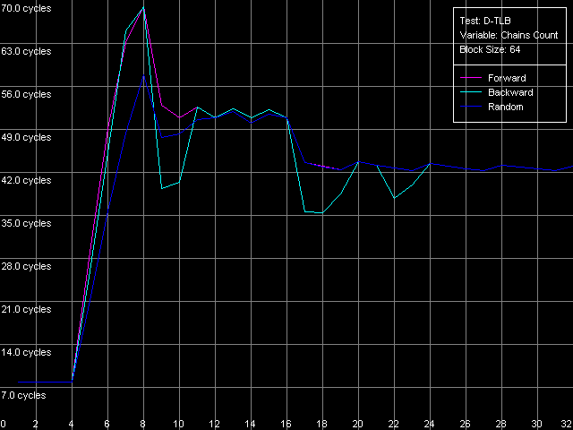 AMD Athlon XP 1800+  AMD Opteron 244 The L1 access latency when only L2 D-TLB is used sharply increases at the number of chains over 4. It means that the L2 D-TLB in these processors is 4-way associative. I-TLB level parametersI-TLB parameters will be measured the way we used for D-TLB. I-TLB Size preset in I-TLB test is used to measure the I-TLB size (level structure).  AMD Athlon XP 1800+  AMD Opteron 244 For Opteron we modified the standard preset by increasing the maximum number of TLB Entries up to 1024. Both processors have two I-TLB levels. The first level (L1 I-TLB) in AMD K8 was twice increased (up to 32 entries) compared to the previus-generation architecture K7. The L2 I-TLB was expanded up to 512 entries in the newer architecture. Nevertheless, both processors have the same I-TLB level interaction organization which we call inclusive, like for D-TLB. To estimate associativity of every I-TLB level we will take I-TLB Associativity, 16 Entries preset. For AMD K7 the number of I-TLB entries used will be decreased to 15 in order not to exceed the bounds of L1 I-TLB (since one of its entries is concerned with addressing of the test code page).  AMD Athlon XP 1800+ 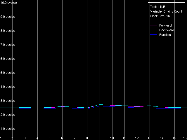 AMD Opteron 244 The L1 I-TLB in both cases is fully associative. Let's estimate associativity of the second level of I-TLB. Presets: I-TLB Associativity, 32 Entries for K7, and I-TLB Associativity, 128 Entries for K8. 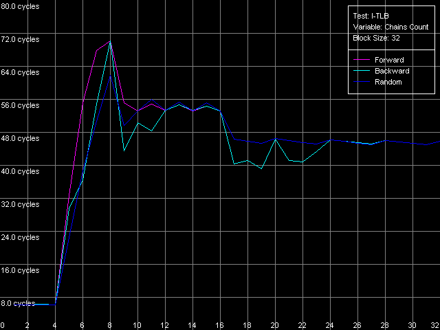 AMD Athlon XP 1800+ 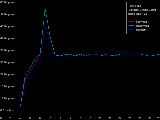 AMD Opteron 244 In both cases the results match the L2 I-TLB associativity specified which equals 4. ConclusionToday we carried out the first thorough low-level test of AMD K7/K8 platforms
using the universal RightMark Memory Analyzer. The results show that this
test suite can be successfully used for estimation of key low-level platform
parameters. Next time we will continue our examination and test the Intel
Pentium 4 platform.
Dmitry Besedin (dmitri_b@ixbt.com)
Write a comment below. No registration needed!
|
Platform · Video · Multimedia · Mobile · Other || About us & Privacy policy · Twitter · Facebook Copyright © Byrds Research & Publishing, Ltd., 1997–2011. All rights reserved. | |||||||||||||||||||||||||||||||||||||||||||||||||||||||||||||||||||||||||||||||||||||||||||||||||||||||||||||||||||||||||||||||||||||||||||||||||||||||||||||||||||||||||||||||||||||||


