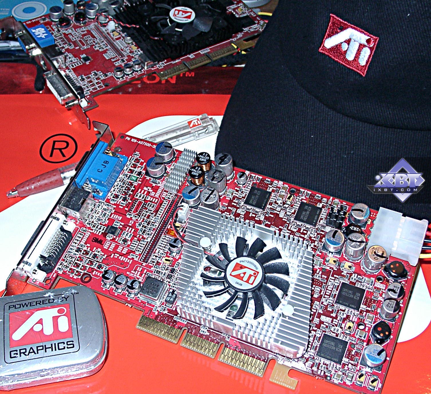
ATI RADEON 9800 PRO 128MB
|
No sooner had we received NVIDIA's GeForce FX 5600 (NV31) and GeForce FX 5200 (NV34) and tested High-End GeForce FX 5800 (NV30), than ATI Technologies
attacked again and announced a new-generation line of video accelerators.
As you will see later, the new line comprises the modified and improved products:
- RADEON 9800 PRO -- 380 MHz chip, 128MB 340 MHz (DDR 680) 256-bit local memory
- RADEON 9800 -- 325? MHz chip, 128MB 310? MHz (DDR 620?) 256-bit local memory
- RADEON 9600 PRO -- 400? MHz chip, 128MB 300? MHz (DDR 600) 128-bit local memory
- RADEON 9600 -- 350? MHz chip, 64/128MB 275? MHz (DDR 550) 128-bit local memory
- RADEON 9200 PRO -- 275 MHz chip, 64/128MB 275 MHz (DDR 550) 128-bit local memory
- RADEON 9200 -- 250 MHz chip, 64/128MB 200 MHz (DDR 400) 128-bit local memory

The two latter products are actually copies of the RADEON 9000/PRO with added AGP 8x support. The marketers again gave a higher number of 9200 to the chip weaker than RADEON 9100 (former RADEON 8500LE). Nobody knows the precise specs of 9600 and 9600 PRO, but reportedly, they will be a half of 9800/Pro (4 pixel and 2 vertex pipelines). The rumor has it that 9600/PRO will perform worse than 9500/PRO. When they come out on the market, we will test them thoroughly, but the symptoms are alarming, because NVIDIA's latest mainstream and low-sector products (NV31/34) successfully fight against RADEON 9500/PRO line in the heavy modes (AA and anisotropy).
But time will tell. Today we still deal with the High-End solution. By the way, is RADEON 9800 PRO something new regarding technologies and
3D functions, or it is just an overclocked version of RADEON 9700 PRO?
I hope this review will give us the answer. By the way, here is a list of reviews of RADEON 9700/9700 PRO revealing all features and peculiarities
of ATI's previous High-End product:
- Analysis of RADEON 9700 architecture and Microsoft DirectX 9.0
- ATI RADEON 9700 Pro 128MB Review
- MAYA II R9700Pro 128MB -- performance estimated on the new Pentium 4 2.53 GHz based platform, comparison with the NVIDIA's 40.41 driver
- Hercules 3D Prophet 9700 Pro 128MB -- new CATALYST 2.3 driver estimated in 3DMark2001 SE,
and Unreal Tournament 2003 DEMO final release
- PowerColor Evil Commando2 RADEON 9700 Pro 128MB -- performance of the new CATALYST 2.3 driver estimated in game tests, 3D quality issues
- Sapphire Atlantis RADEON 9700 Pro 128MB -- detailed analysis of anisotropic filtering
of the RADEON 9700
- ATI RADEON 9700, RADEON 9500 64MB and Gigabyte MAYA II RADEON 9500 64MB
- Sapphire Atlantis RADEON 9500 128MB -- 256-bit memory bus of RADEON 9500 128MB!
DOOM III tests
- HIS Excalibur RADEON 9700 Pro and tests in the DirectX 9.0 RC0
- ATI RADEON 9500 PRO -- 128-bit memory bus and buffer compression in AA mode (virtual 256-bit
bus)
- ATI RADEON 9500 64MB, 9500 128MB, 9500 PRO, 9700 and 9700 PRO in DirectX 9.0: Part 1 -- Game tests and 3DMark2001, as well as Soft9700!
- ATI RADEON 9500 64MB, 9500 128MB, 9500 PRO, 9700 and 9700 PRO in DirectX 9.0: Part 2 -- Tests in DirectX 9.0 -- synthetic tests from RightMark 3D
- YUAN XpertVision RADEON 9000 64MB and RADEON 9700 PRO
- Sapphire Atlantis RADEON 9700 & RADEON 9700 PRO Ultimate Edition
RADEON 9800 PRO specification at the time of its announcements:
- Fab process: 0.15 micron
- Transistors: 115 M
- Core clock speed: 380 MHz
- Memory bus: 256-bit DDR (DDR II will possibly be supported later)
- Local memory size: up to 256 MB
- Memory clock speed: 340 DDR (680) MHz, 24 GB/s bandwidth
- Interface bus: AGP 8x, 2 GB/s bandwidth
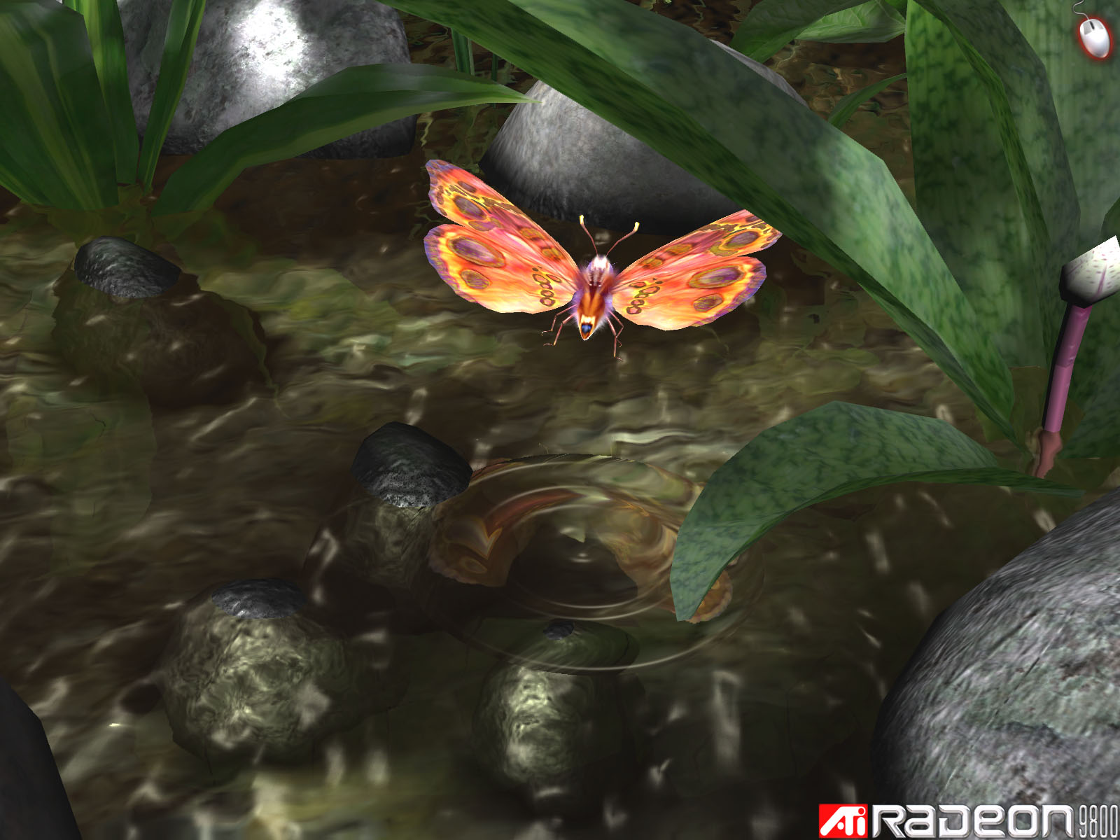
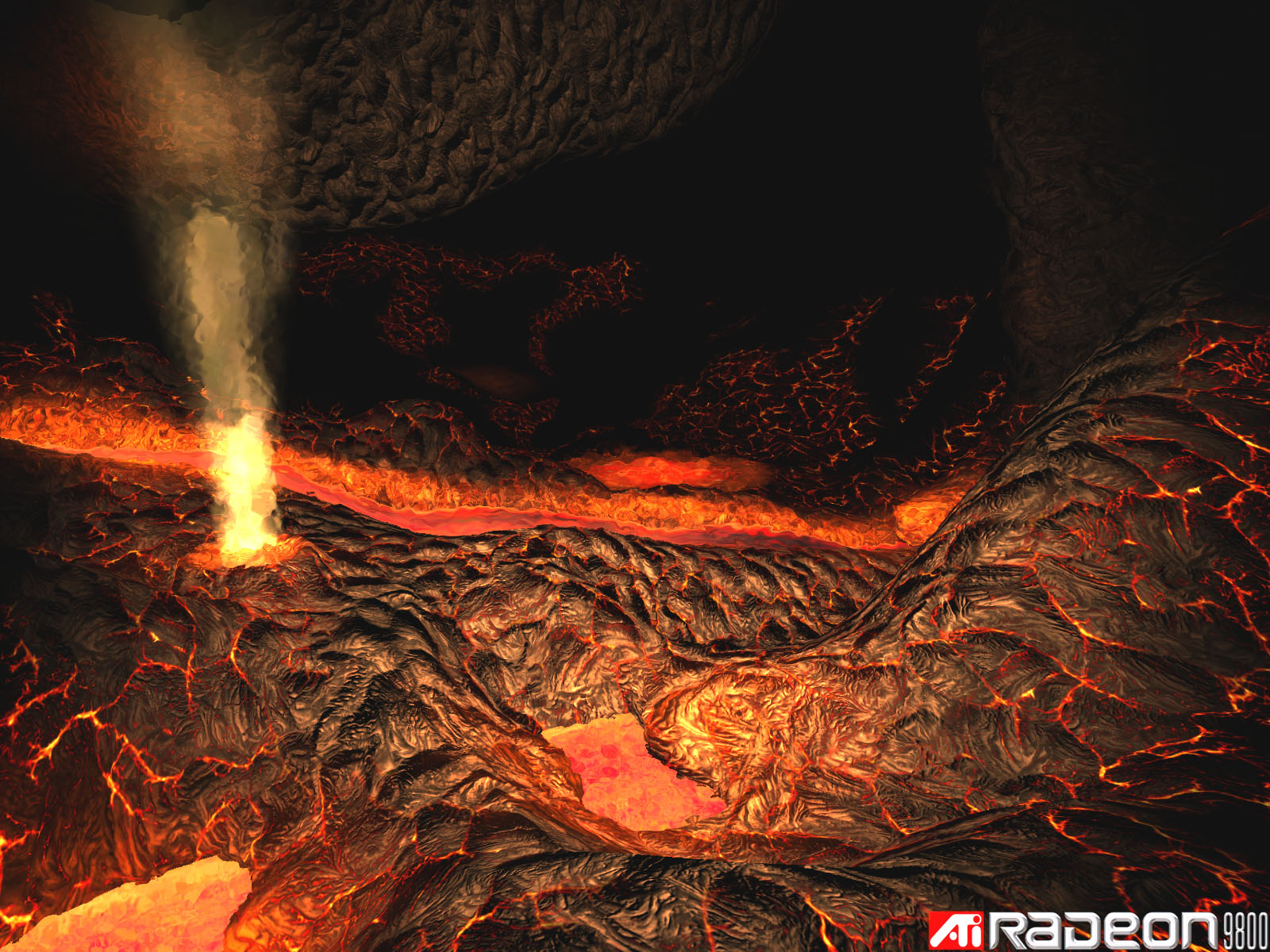
- Full support of DX9's main features:
- Floating-point 64 and 128-bit data formats for textures (including 3D and cubic textures) and frame buffer (vectors of 4 components of F16 or F32)
- Pixel pipelines with floating-point arithmetics (F24[4] or F24[3+1] calculations)
- Pixel Shaders 2.0
- 4 independent vertex pipelines
- Vertex Shaders 2.0
- N-Patches hardware tessellation with Displacement Mapping, and, if possible, adaptive detail level
- New F-buffer technology supports almost unlimited pixel shaders
- 8 independent pixel pipelines
- 8 texture units (one for pixel pipeline) supporting trilinear filtering without speed loss and a combination of anisotropic and trilinear filtering
- 4-channel (4 64-bit channels) memory controller connected to the accelerator's core and AGP switch on the peer-to-peer basis
- HyperZ III+ memory optimization technology (Fast Z Clear and 8x8 depth buffer compression, Hierarchical Z Buffer for fast visibility checking)
- Additional optimizations for speedy operation of the double-side stencil buffer
- Early Z test (pixel shaders work only for visible pixels)
- Hardware acceleration of MPEG 1/2 unpacking and compression, VIDEOSHADER technology (arbitrary processing of a video flow with pixel shaders)
- Two independent CRTC
- Two built-in 10bit 400 MHz RAMDAC with hardware gamma correction
- Integrated TV-Out
- Integrated DVI (TDMS transmitter) interface, up to 2043*1536
- Integrated general-purpose digital interface for external RAMDAC or DVI transmitter and for coupling with TV tuner
- FC packaging (FlipChip)
The characteristics are similar to the previous flagship R300. There are two main differences: optimization of operation with the double-side stencil
buffer booting performance in DOOM III engine based games and the like which actively use stencil buffer based dynamic shadows, and special logic
in the pixel processors.
This approach makes possible to store in the local memory both final color values calculated by the pixel shader and intermediate values of parameters. It's called F-buffer and requires rather simple chip support (to record and restore the flow of parameters) and a special compiler.
This approach allows executing almost unlimited shaders dividing them into parts each of which works independently over a certain screen area and records intermediate parameters for each pixel from this area which are then delivered into the F-buffer for the next shader part. The next shader part reads the parameters in the order they were recorded in, continues calculations and writes down new parameters. This approach is more advantageous than the multipass image rendering. But its support is yet planned only for OpenGL driver.
This technology is meant for realistic graphics and DCC -- games are still far from enabling all capabilities of even standard pixel shaders 2.0 limited by 64 computing operations.
In this material the F-buffer technology is closely examined (FIFO-stream buffer).
Write a comment below. No registration needed!
|
|
 |
|
|
|