NVIDIA announces GeForce FX
Yesterday NVIDIA announced the release of new generation GPUs, formerly codenamed NV30 and officially named NVIDIA GeForce FX.
Naturally, this release is a major step for the graphics industry:
- GPU core about 125 million transistors
- Process — 0.13-micron
- 3 geometry processors — more than enough for DX9 VS 2.0
- 8 pixel processors — more than enough for DX9 PS 2.0
- 128-bit DDR II interface
- 4-channel switching memory controller

- Local memory bandwidth saving technology, including the complete color and depth buffer compression (world-first 4:1 compression)
- Programmable array of 16 texture filter blocks, up to 8 selected and filtered per tick
- AGP 3.0 (8õ)
- Tile optimization: caching, compression, HSR
- High integer (10/16-bit per component) and floating point (16/32-bit per component) precision of texture and frame buffer
- 32-bit floating point operations, new adaptive anisotropic filtering to reduce FPS falloffs
- Up to 128x anisotropy
- New ÀÀ modes — MSAA 8õ and hybrid MS/SSAA 6x
- Frame buffer compression
- Dual 400MHz RAMDACs
- External TV-Out interface
- Dual TDMS for external DVI
- Meeting AGP 3.0, GeForce FX enables to make cards without external power
All willing to get acquainted with the new architecture and features of GeForce FX should read our new (very good) review NVIDIA GeForce FX or "Cinema show started". And finally the photo of reference GeForce FX.
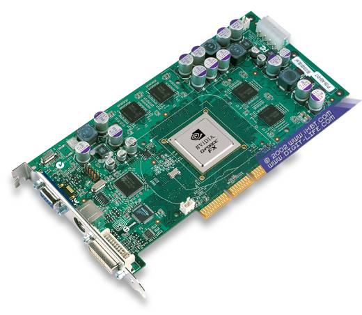
Note 128MB of 128-bit DDR II (8 Samsung chips, 1 GHz DDR), external power connector. DVI, TV-Out, and VGA output. The official GPU clock is 500MHz, but it should raise in the future, I guess. Though read about it in the review.
Write a comment below. No registration needed!
|
|


