 |
||
|
||
| ||
|
||
|
||
| ||
Part 1: Theory and architectureIn our previous article devoted to the NVIDIA GeForce 8800 GT (G92) we mentioned that the solution was based on a GPU, where not all ALUs and TMUs were unlocked. Some of them were waiting to be unlocked in a more expensive card. This time has come - NVIDIA has announced an overhauled GeForce 8800 GTS with the same name as the cheaper G80-based solution. You can distinguish this card by memory size - 512 MB, unlike 320 MB and 640 MB modifications of the older card. This card is named GeForce 8800 GTS 512MB. The new modification of the GeForce 8800 GTS is based on the G92, which is also used in the GeForce 8800 GT (Upper Mid-End card). So we already know the key features. Unlike two GeForce 8800 GT cards with the recommended price of $200 - $250 (which does not agree with real prices, by the way), the new solution has the recommended price of $349-399. This GPU supports only a 256-bit memory bus, but it has more unlocked unified processors. Let's examine the new Lower High-End card from NVIDIA... Before you read this review, you should look through the baseline theoretical articles - DX Current, DX Next, and Longhorn. They describe various aspects of modern graphics cards and architectural features of NVIDIA and AMD's products.
These articles predicted the current situation with GPU architectures, a lot of forecasts on future solutions came true. Detailed information on the unified architecture of NVIDIA G8x/G9x (by the example of older GPUs) can be found in the following articles:
As we mentioned in our previous article, G92 includes all advantages of G8x: unified shader architecture, full support for DirectX 10, high-quality anisotropic filtering and CSAA 16x. Some units of this GPU are a tad different from those in the G80. But the main change is the 65 nm fabrication process, which allows to reduce the manufacturing costs. Let's analyze characteristics of this GPU and new graphics cards: GeForce 8800 GTS 512MB
Reference GeForce 8800 GTS 512MB Specifications
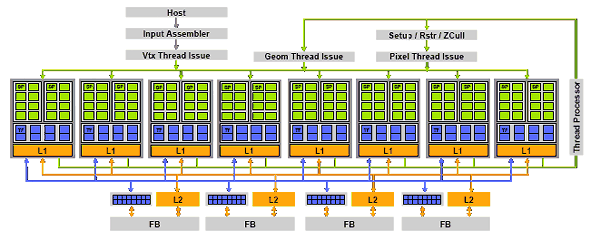
The new modification of the GeForce 8800 GTS 512MB differs much from the old products. The number of execution units is increased (ALUs and TMUs), GPU clock rate has grown much as well, including the frequency of shader units. Even though the memory bus is cut down (256-bit versus 320-bit in the old modifications), memory bandwidth remains the same, because its frequency is raised. As a result, the new GTS card executes shaders and fetches textures much faster. At the same time, the fill rate and memory bandwidth are the same. As the bit capacity of the memory bus has changed, the memory size cannot be 320 MB or 640 MB - only 256 MB, 512 MB, or 1 GB. The first value is too small, it will be insufficient for such a card. The last value is too big, an insignificant performance gain will hardly justify the increased prices for such modifications (they may appear in future). So NVIDIA has chosen a medium option with 512 MB. Our recent analysis has demonstrated that it's a golden mean for all modern games, which have high requirements to video memory and use up to 500-600 MB. It does not mean that all resources of a game must be stored in local video memory only. Resource management may be given to API, especially considering video memory virtualization available in Direct3D 10. ArchitectureAs we wrote in the older review of the GeForce 8800 GT, the G92 is actually a modified old flagship G80 manufactured by the new fabrication process. The new GPU has eight big shader units and 64 texture units, as well as four wide ROPs. In spite of all improvements, the number of transistors in a GPU seems too high. Perhaps, complexity of the chip is increased, because it now contains a video processor of the new generation and NVIO, which used to be a stand-alone chip. Besides, the number of transistors is affected by more complicated TMUs. Perhaps, caches were also enlarged for higher efficiency of the 256-bit memory bus. There are just a few architectural changes in G92. All of them were covered in the previous article, and we shall not repeat ourselves. Everything we wrote in previous reviews holds true. We'll publish the main diagram of the G92, now with all 128 unified processors:
 What differs from G80 is fewer ROPs and modified TMUs (we wrote about the changes in our previous review.) We repeat that 64 texture units in the GeForce 8800 GTS 512MB in real applications will NOT be faster than 32 units in the GeForce 8800 GTX in most cases. When trilinear and/or anisotropic filtering are enabled, their performance will be similar, because they have the same number of texture filter units. The cards based on the G92 will be faster, of course, when non-filtered texture fetches are used. PureVideo HDOne of the expected changes in the G92 is the built-in video processor of the second generation, which was also used in the G84 and G86, with extended support for PureVideo HD. This video processor offloads a CPU almost completely in video decoding tasks of all types, including such "heavy" formats as H.264 and VC-1. The G92 uses a new model of the programmable PureVideo HD processor, which also includes the so-called BSP engine. The new processor can decode H.264, VC-1, and MPEG-2 formats with the resolution of up to 1920x1080 and the bitrate of up to 30-40 Mbit/s. It does all the work on decoding CABAC and CAVLC data on the hardware level, so you can play all existing HD-DVD and Blu-ray discs even on mediocre single-core PCs. The new processor does not decode VC-1 as effectively as H.264, but it can still do it. You can read the details about the video processor of the second generation in our reviews of the G84/G86 and the G92. Links to these articles are published in the beginning of the article. PCI Express 2.0What concerns true innovations of the G92, we can mention PCI Express 2.0. The second version of PCI Express doubles the standard throughput, from 2.5 Gbit/s to 5 Gbit/s. As a result, the x16 slot can transfer data at up to 8 GB/s in each direction, unlike 4 GB/s for Version 1.x. What's really important, PCI Express 2.0 is compatible with PCI Express 1.1. Old graphics cards will work in new motherboards, and new graphics cards supporting the second specifications will work in motherboards without this support. Provided the external power is sufficient and the interface bandwidth is not increased, of course. NVIDIA's competitor evaluated the real effect of higher PCI Express throughput on performance. According to its articles, a Mid-End graphics card with 256 MB of memory becomes 10% as fast in such games as Company of Heroes, Call of Juarez, Lost Planet, and World In Conflict, when you upgrade from PCI Express 1.0 to 2.0. The results vary from 5% to 25% depending on a game and test conditions. Of course, we speak of high resolutions, when the frame buffer and contiguous buffers take up most of the local video memory, and some resources are stored in system memory. Specifications 2.0 support both 2.5 Gbit/s and 5 Gbit/s transfer rates for backward compatibility with existing PCI Express 1.0 and 1.1 solutions. Backward compatibility of PCI Express 2.0 allows to use old 2.5 Gbit/s cards in 5.0 Gbit/s slots, which will work at a lower speed. And new devices will support both 2.5 Gbit/s and 5 Gbit/s transfer rates. Theoretically, compatibility is full. But in practice you may run into problems with several combinations of motherboards and expansion cards. Support for external interfacesThere are no differences from the GeForce 8800 GT in this respect. The NVIO chip installed in the GeForce 8800 cards to support external interfaces (2x400 MHz RAMDAC, 2xDual Link DVI (or LVDS), HDTV-Out) is now integrated into the GPU. So the support for all these interfaces is built into the G92. The GeForce 8800 GTS 512MB cards are usually equipped with two Dual Link DVI outputs with HDCP support. What concerns HDMI, support for this connector is implemented. It can be used by manufacturers in non-reference graphics cards. However, a graphics card should not necessarily have an HDMI port, it can be replaced with a DVI-HDMI adapter, which is included into most modern bundles. The next part of this article will be devoted to synthetic tests of the new solution from NVIDIA. Write a comment below. No registration needed!
|
|
Platform · Video · Multimedia · Mobile · Other || About us & Privacy policy · Twitter · Facebook
Copyright © Byrds Research & Publishing, Ltd., 1997–2011. All rights reserved.


