|
||
|
||
| ||
|
||
|
||
| ||
Part 2: Graphics Card Features (Including BFG Cards) And Synthetic Benchmarking Results
Glamour factor of synthetic tests:
Divide the amount of GPU transistors by the DX version number. It's getting higher all the time... 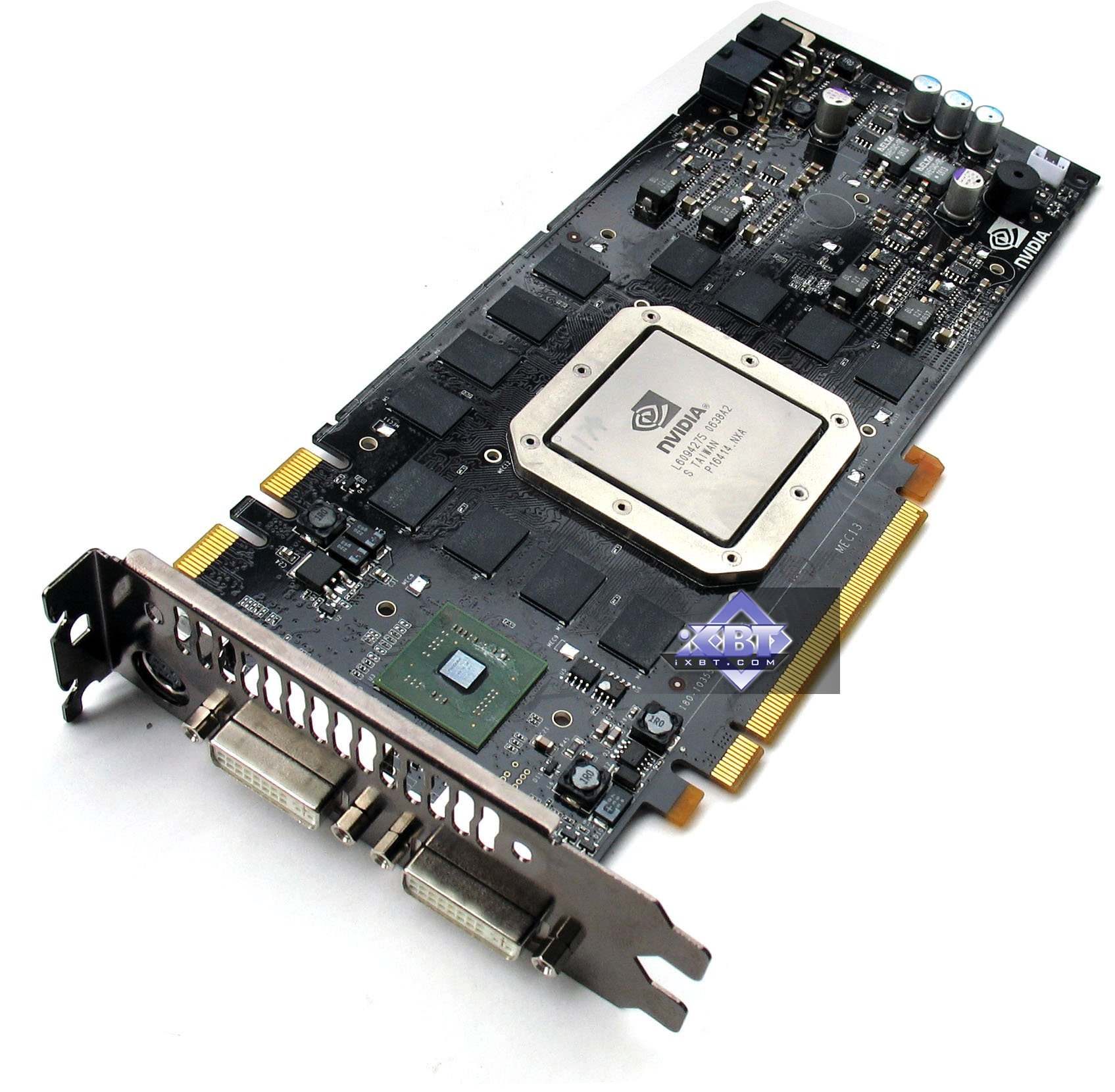 TABLE OF CONTENTS

Alexander Medvedev has already reviewed all architectural peculiarities of the new products in Part I. We know that the new line of NVIDIA products currently consists of the following cards:
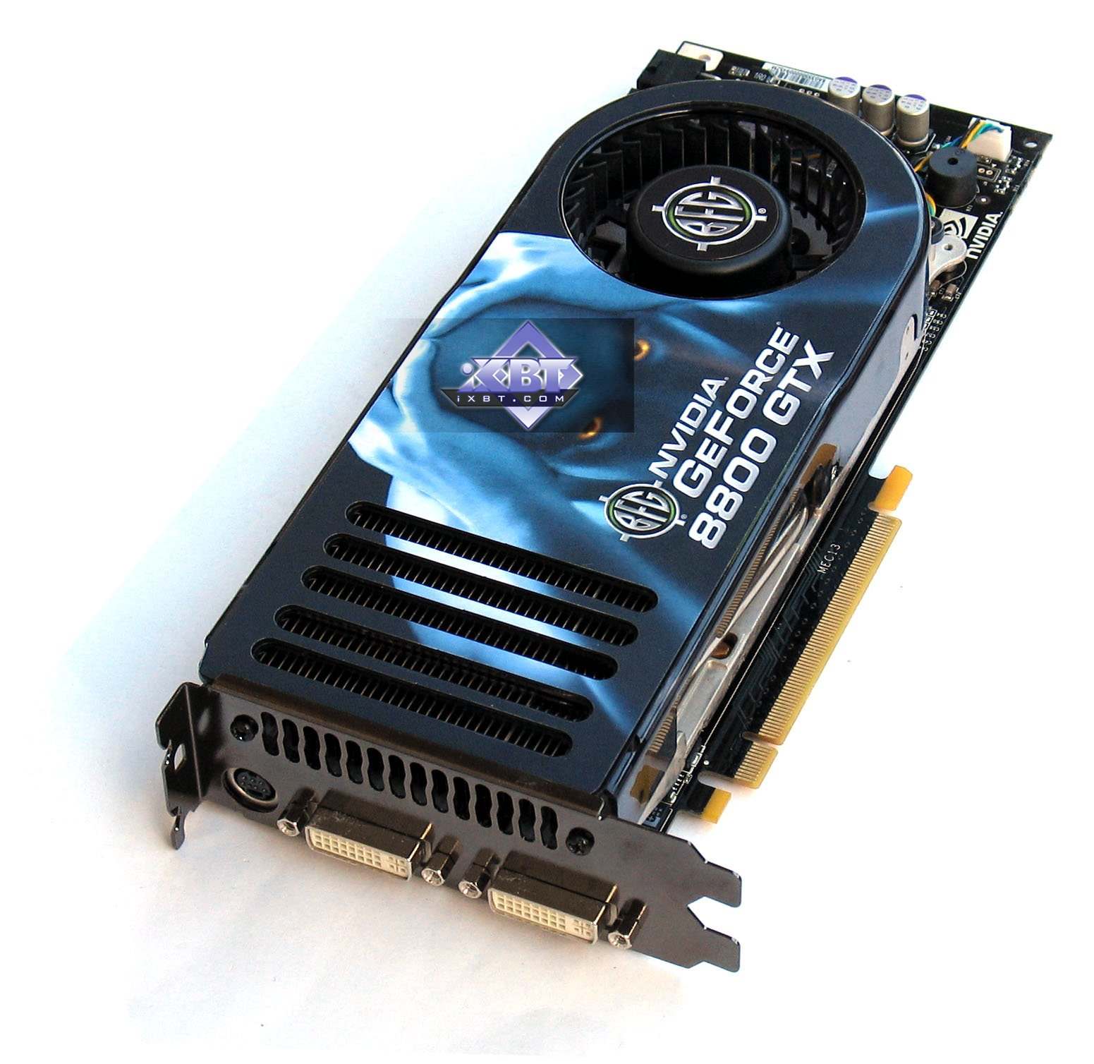
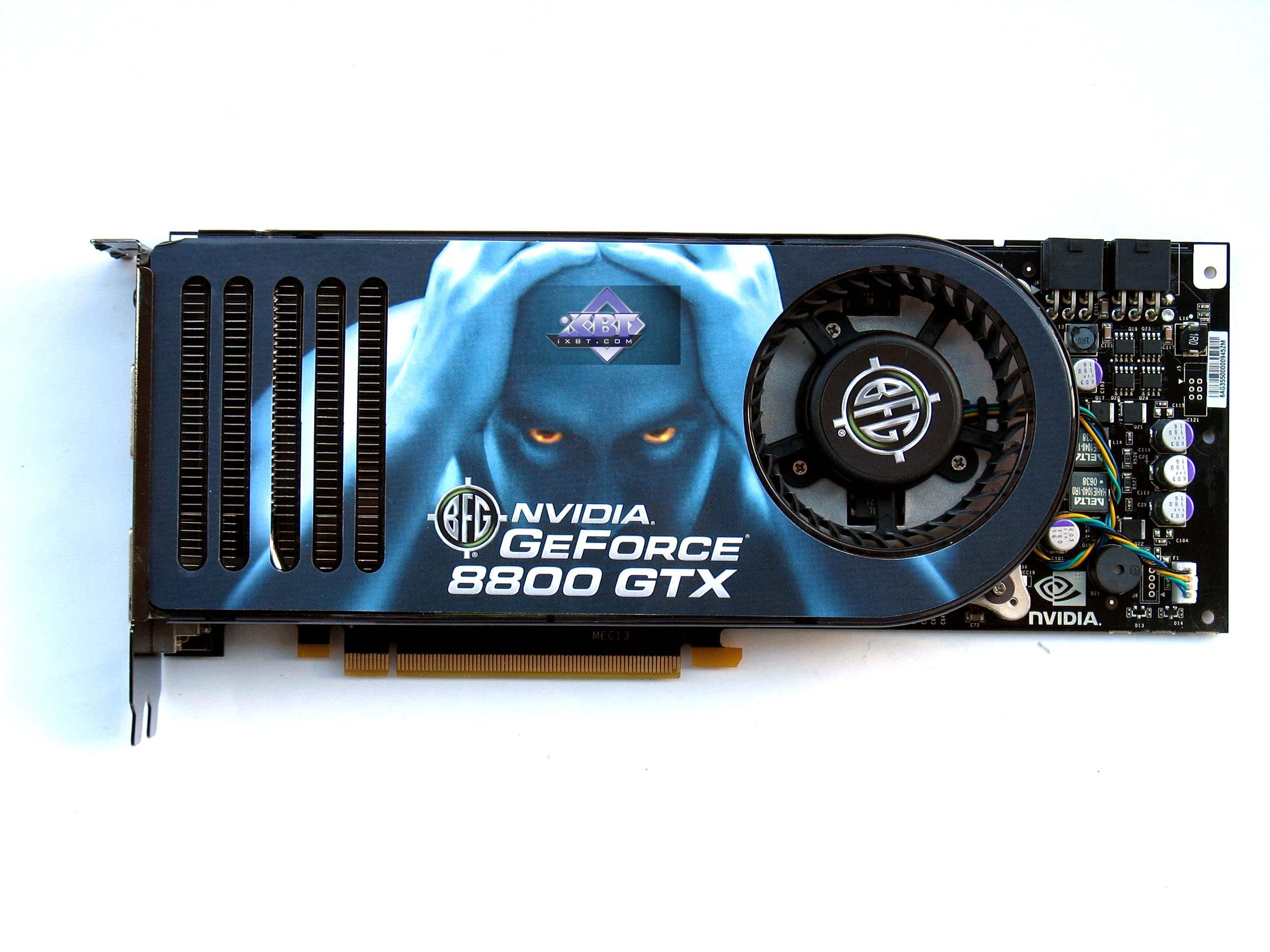
We got our GeForce 8800 GTX at NVIDIA Editor's Day (we'll describe it in Part IV of our article). Then there appeared a card from BFG.
So we had an opportunity to configure SLI:
 But we'll not publish results of the new super tandem yet, because there are still no drivers to support this mode properly. Besides NVIDIA embargoes any publications about 8800 GTX SLI results. Video Cards
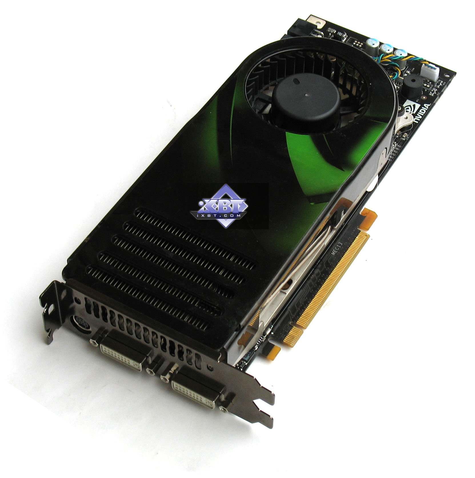
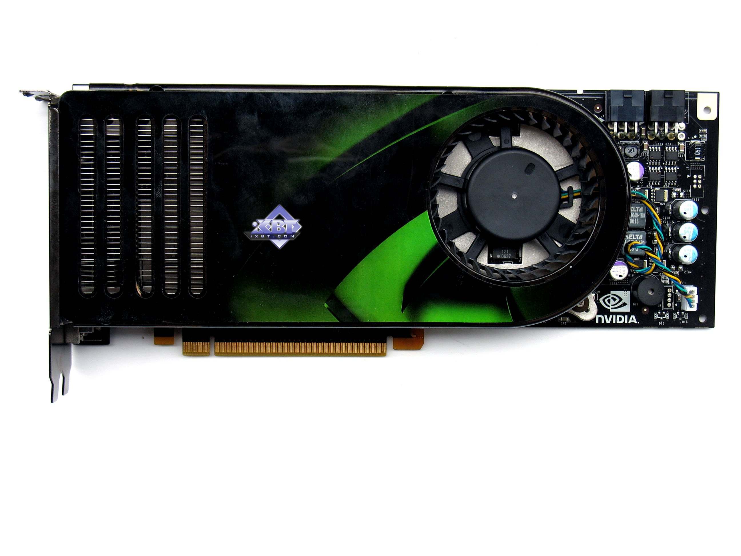
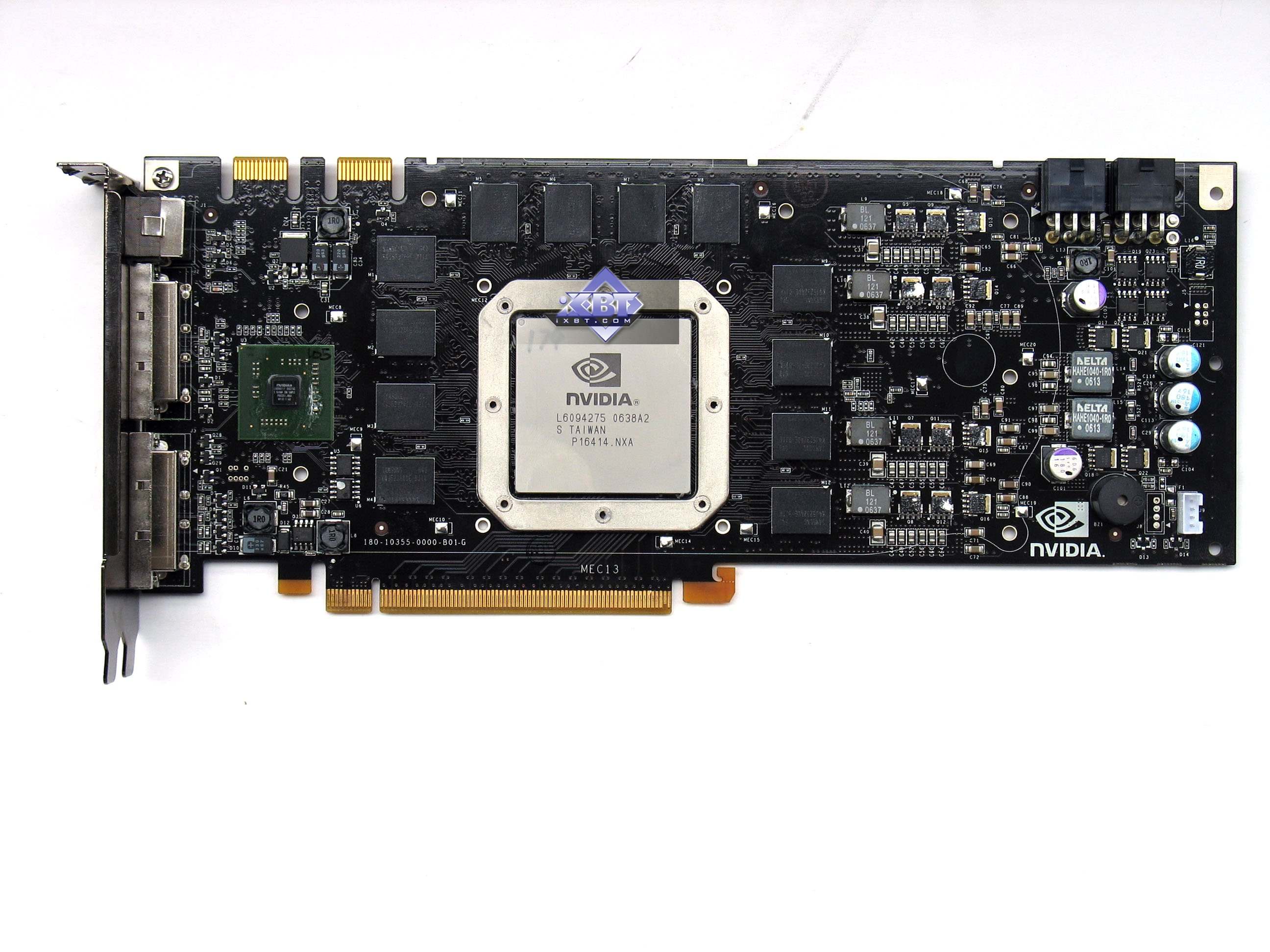
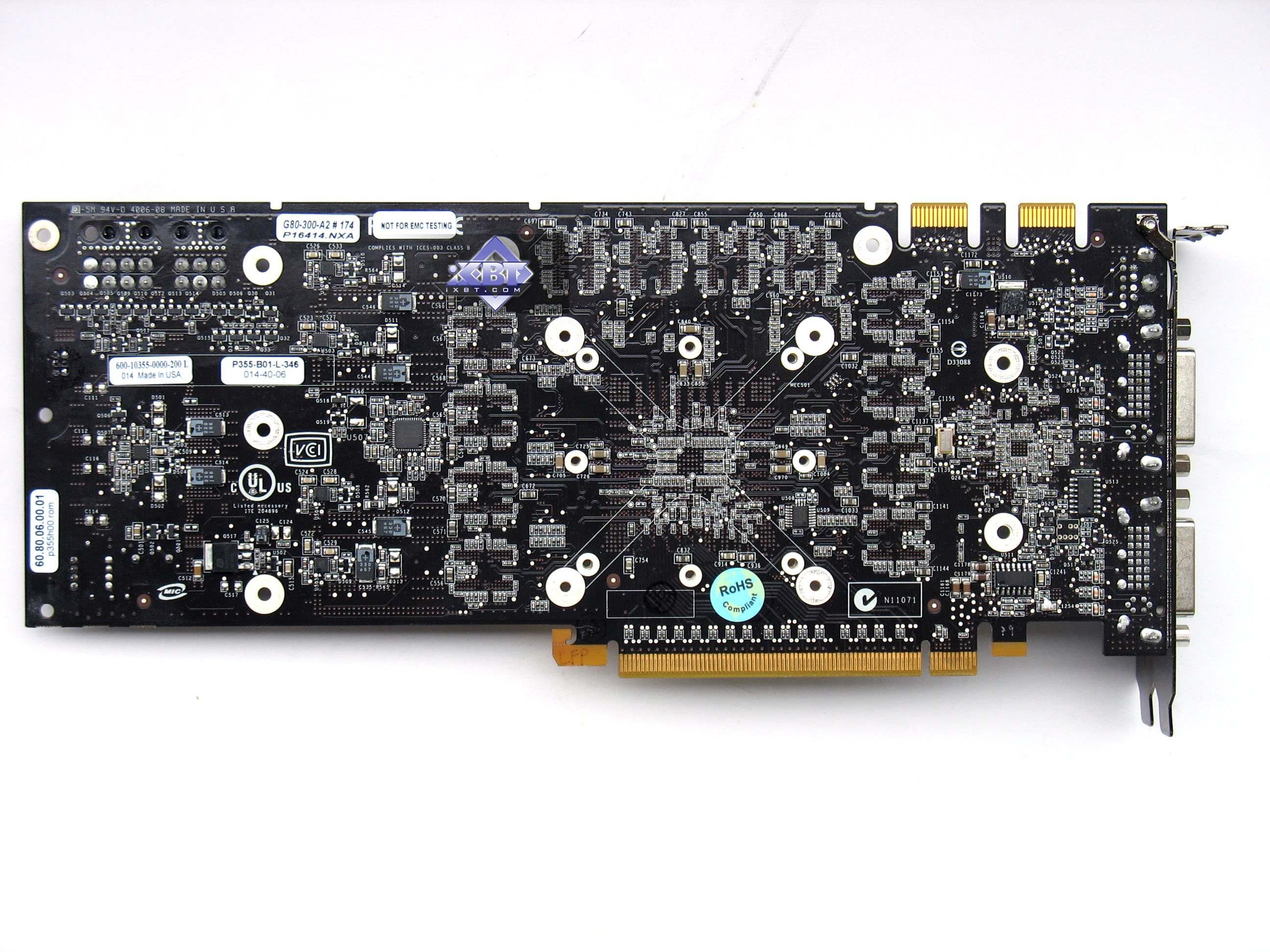
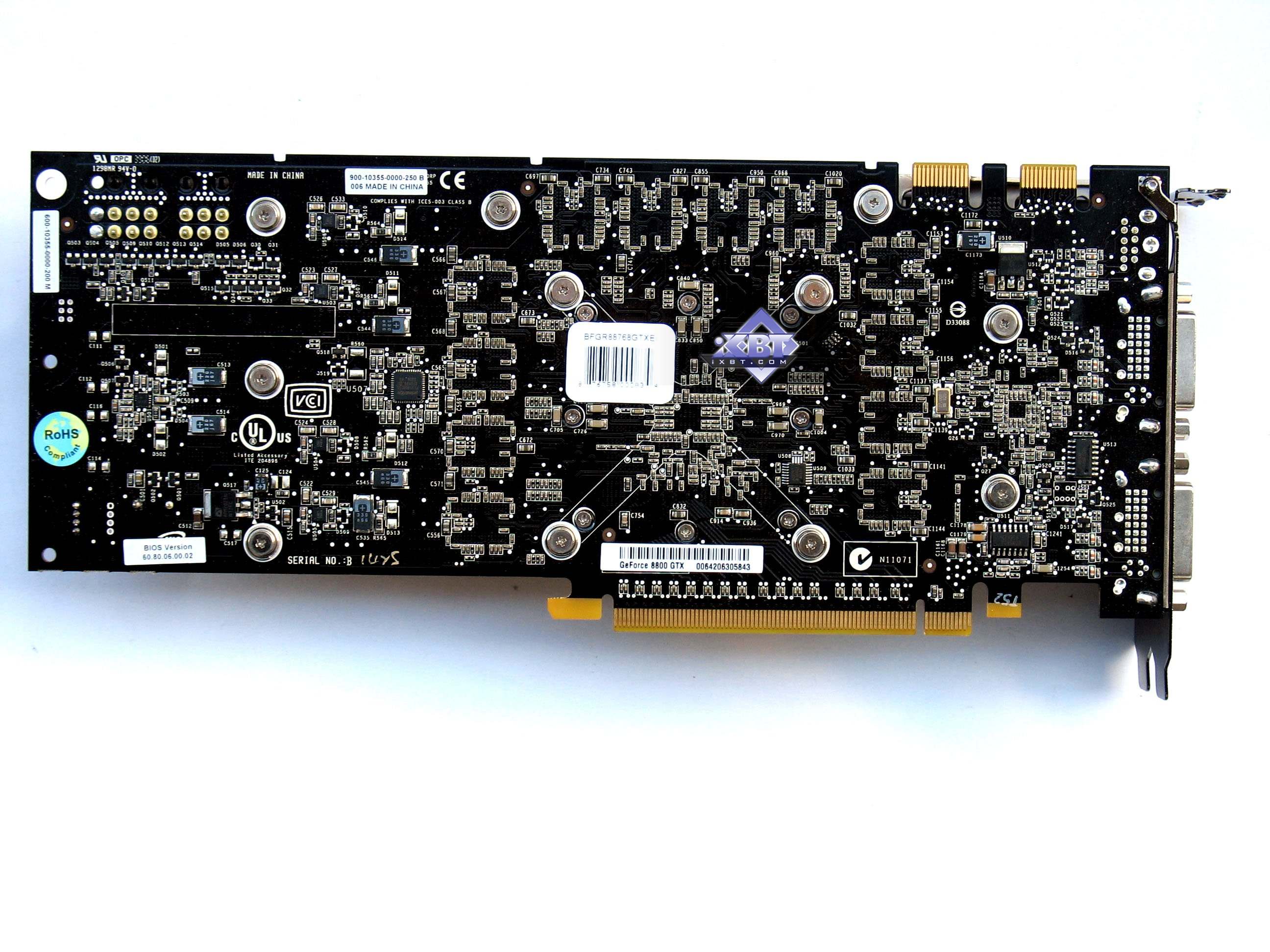
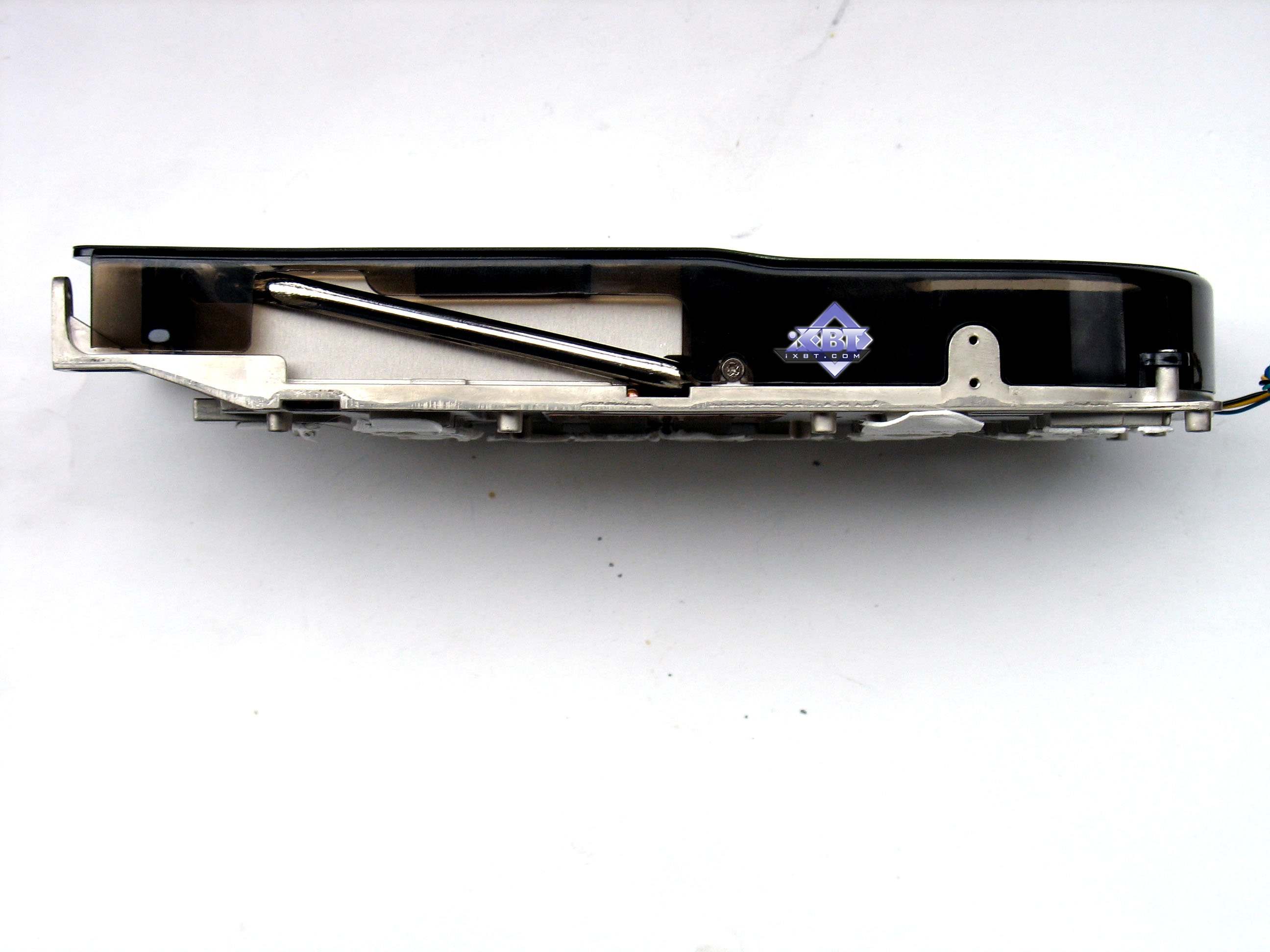
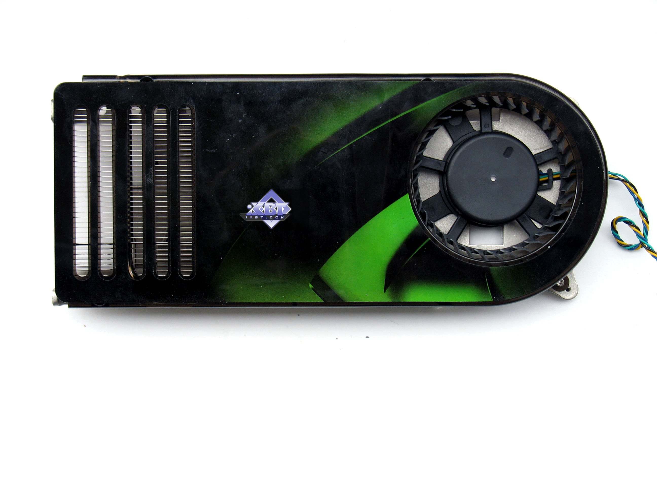
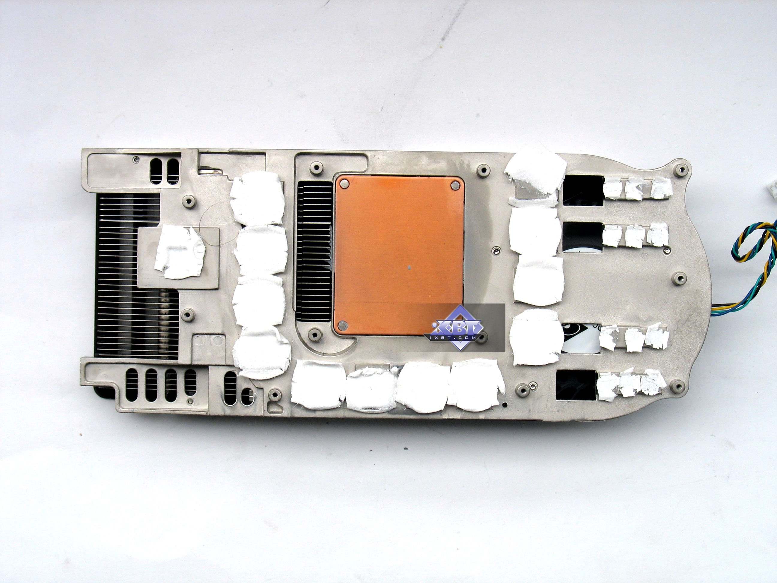
You can see well that the new design of the 8800 cards differs cardinally from the predecessor. As the card has more memory chips, engineers had to give up the semicircular layout of memory chips round the GPU to keep them at the same distance from the processor. So this card uses a rectangular layout of memory chips, which is also used in old solutions. We could see it only in the 7950GX2. But that card (1) had a complex design with two PCBs that applied its limitations, (2) memory operating frequencies were heavily reduced versus the 7900 GTX, for example. In this case the memory frequency is very high, so it was a tough job to design this PCB. Why hasn't the company switched to a double-sided layout of memory chips, placing additional four chips on the back side of the PCB? I guess the problem was in good cooling for these modules, which is unreal to get at the back of the PCB without using complex coolers with heat pipes. So it's better to install all the chips on the front side and cover them with a single heatsink. Note that the PCB is 270mm long, while the usual maximum length used to be 220mm. That is the card has grown by 5cm in length, and it applies certain limitations on using this card even in some modern PC cases. For example, we barely managed to install this card into our testbed with a PC case from ChiefTec, there was only a 5mm gap between the card and a HDD cage. Additional power connectors are expertly placed at the upper edge of the card instead of the butt-end. Speaking of power supply. The photos show that the card requires TWO 6-pin PCI-E cables from a PSU. Users should take it into account. Here are the requirements to a PSU: you need a power supply no less than 450 W (honest!) supporting at least 20A at the 12V line. These are requirements of the GeForce 8800 GTX. By the way, the card itself consumes approximately 150 W under 3D load and about 100 W when idle. The cards have TV-Out with a unique jack. You will need a special adapter to output video to a TV-set via S-Video or RCA (it's usually shipped with the bundle). You can read about TV-Out here. We can see that the cards are equipped with a couple of DVIs. They are Dual link DVI, to get 1600x1200 and higher via a digital connection. Analog monitors with d-Sub (VGA) interface are connected with special DVI-to-d-Sub adapters. Maximum resolutions and frequencies:
We should mention core frequencies separately. Almost all GT/GTX cards used to set core frequencies at 27 MHz steps, frequency of the geometry unit was always higher than those of the other units by 40 MHz. We described it in detail before. But this 27 MHz step was removed in the G71. In the 7900 series, all the three frequencies can be changed at 1-2 MHz steps. A difference between the geometry unit frequency and frequencies of the other units in the 7900 GTX has grown to 50 MHz. This difference in the 7900 GT is 20 MHz, there is no 27 MHz step either. We can see that two available operating frequencies of the G80 core (575 MHz and 1350 MHz) differ greatly. In overclocked mode, when we set ROPs frequency to 625 MHz (increased by 50 MHz), frequency of the shader part grows NOT BY 50 MHz, but proportionally! That is:
Yep! Shader unit frequency has grown by 1118 MHz to 1468 MHz. So ASSUMABLY, overclocking will YIELD BETTER RESULTS. It will certainly please overclockers. What concerns the product from BFG, it's no different, there is just a sticker on the cooler. Speaking of the latter.
Now let's have a look at the processors.
8800 GTX — G80 is manufactured on Week 38, 2006, it's September. That is the chip is just 2 months old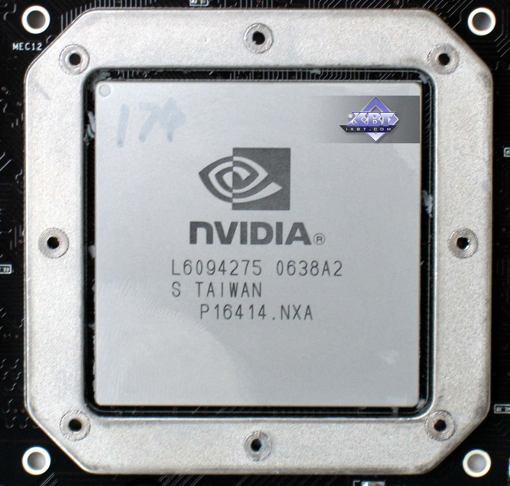 NVIDIA NVIO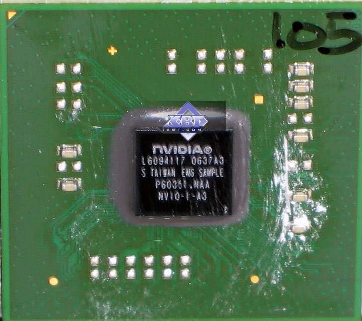 What can I say - I have never seen such huge GPUs! That's the reason why the core is protected from damages with all available means: it's got a cap and even a protective frame around the chip. However, the cap can be used not only to protect the die. It contributes to uniform heat dissipation, because units of the chip operate at very different frequencies. Attentive readers have already seen an additional chip to the left of the main processor. Forum users made wild guesses what it could be. Someone even assumed that it was a second GPU and that G80 consisted of two cores (a more powerful core with a 256-bit bus, and a less powerful one with a 128-bit bus; then NVIDIA summed up these buses to get 384 bit for marketing reasons). Of course, it's not true. All 3D work is done by the only G80 chip with a huge cap. The additional chip on the left is NVIDIA NVIO. It's not "NV10", as it may seem at first glance, it's IO (Input-Output). It would have been strange to see NV10 - GeForce 256 in the new incarnation and manufactured by the new process technology here. :) NVIO is a special chip that incorporates RAMDAC and TDMS. That is the units responsible for outputting graphics to a display or a TV-set were removed from the G80 and added to a separate chip. It's a reasonable solution, because RAMDAC won't be influenced by interferences from a shader unit operating at a high frequency. The same chip is used to support HDCP. While the reference card has no bundle or box, the product from BFG has both.
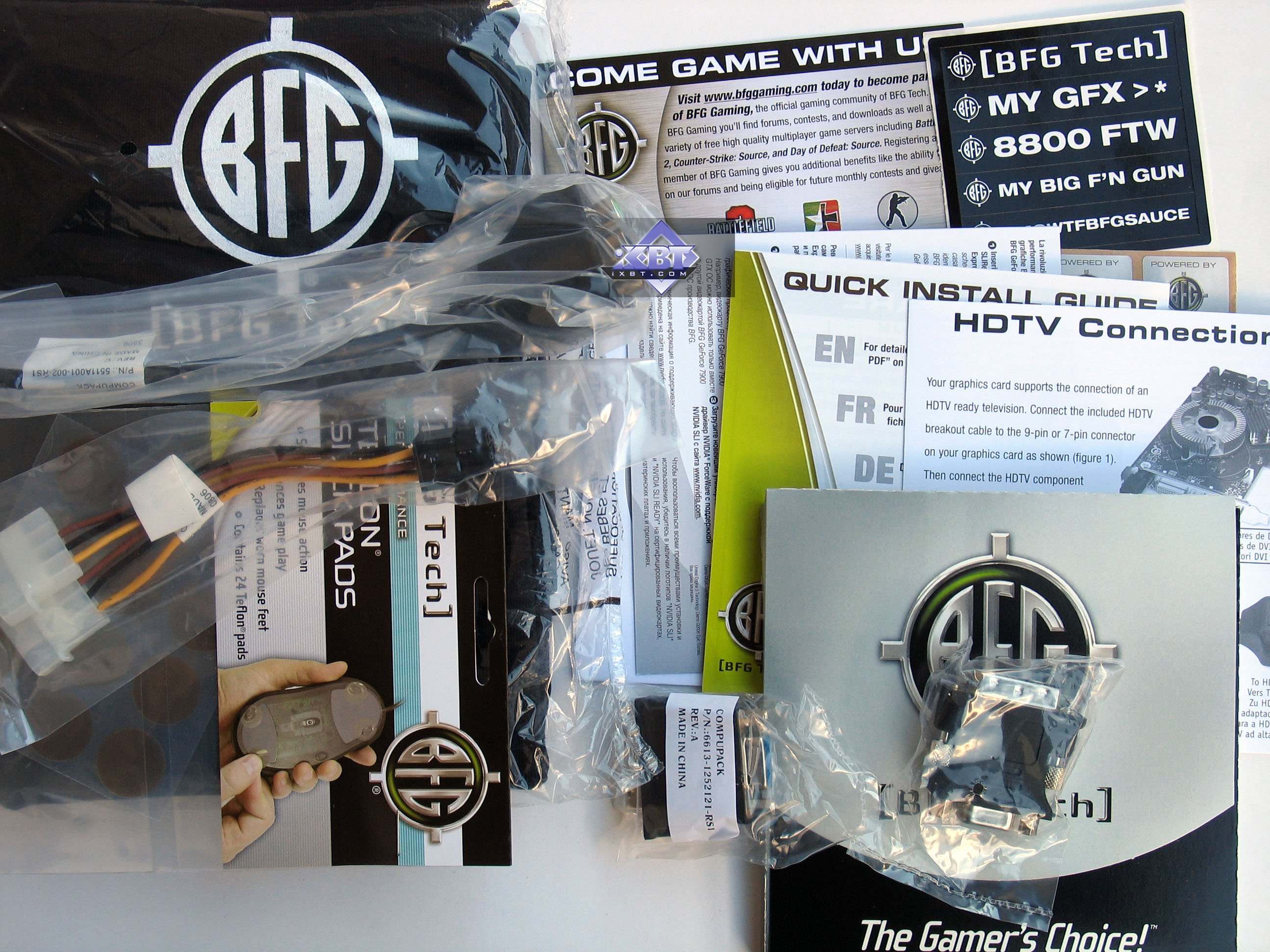
Bundle
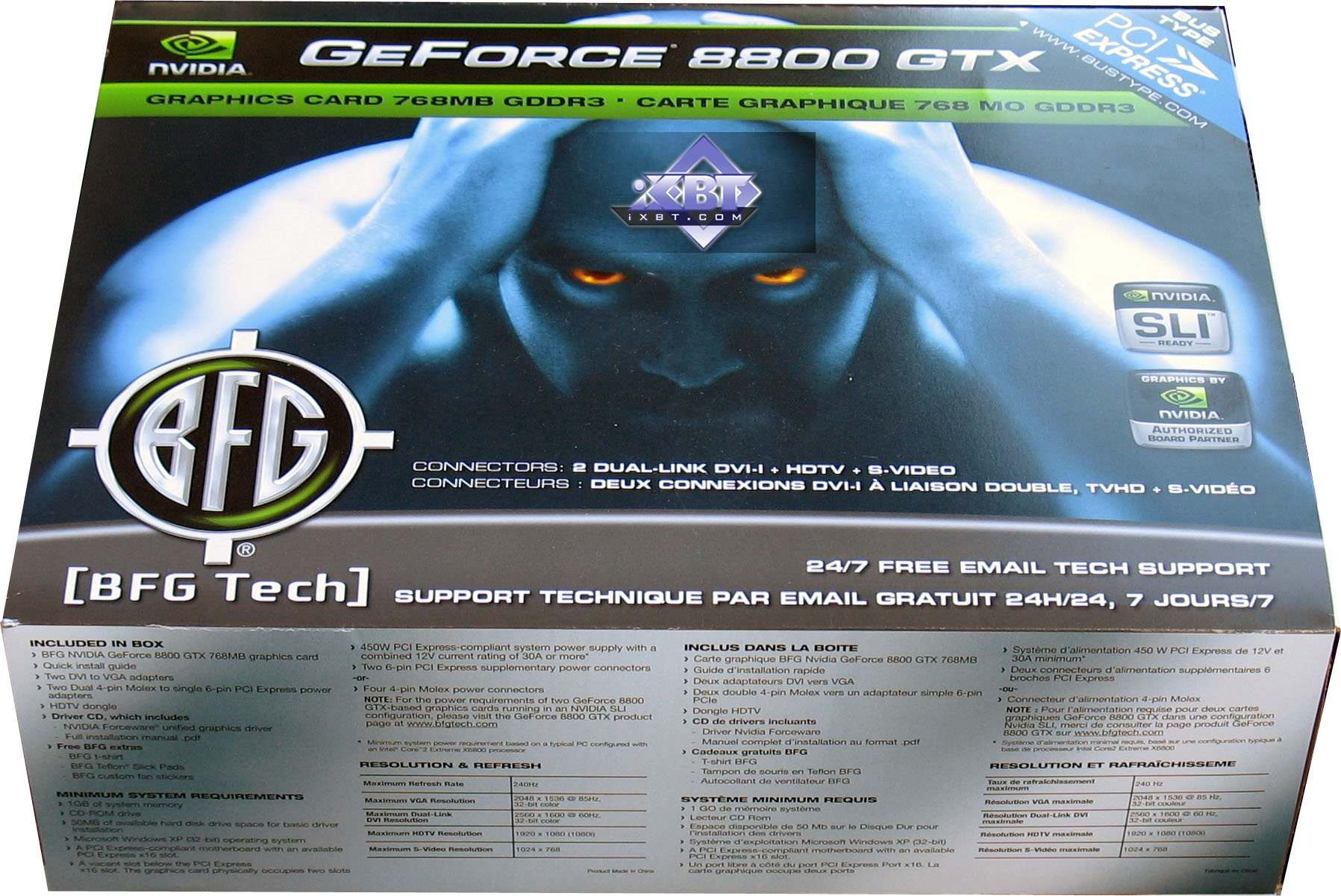
Box.
We should examine the new power supply unit, which we got from NVIDIA together with the 30" monitor for sterling tests of super powerful accelerators of the latest generation. It is a power supply unit from TAGAN, 1100W. 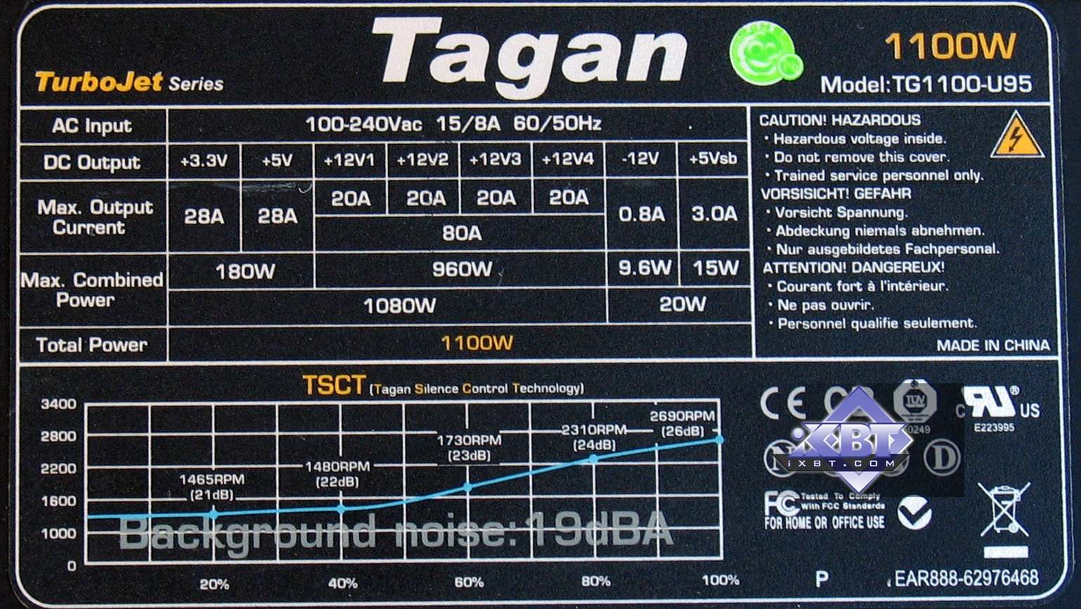 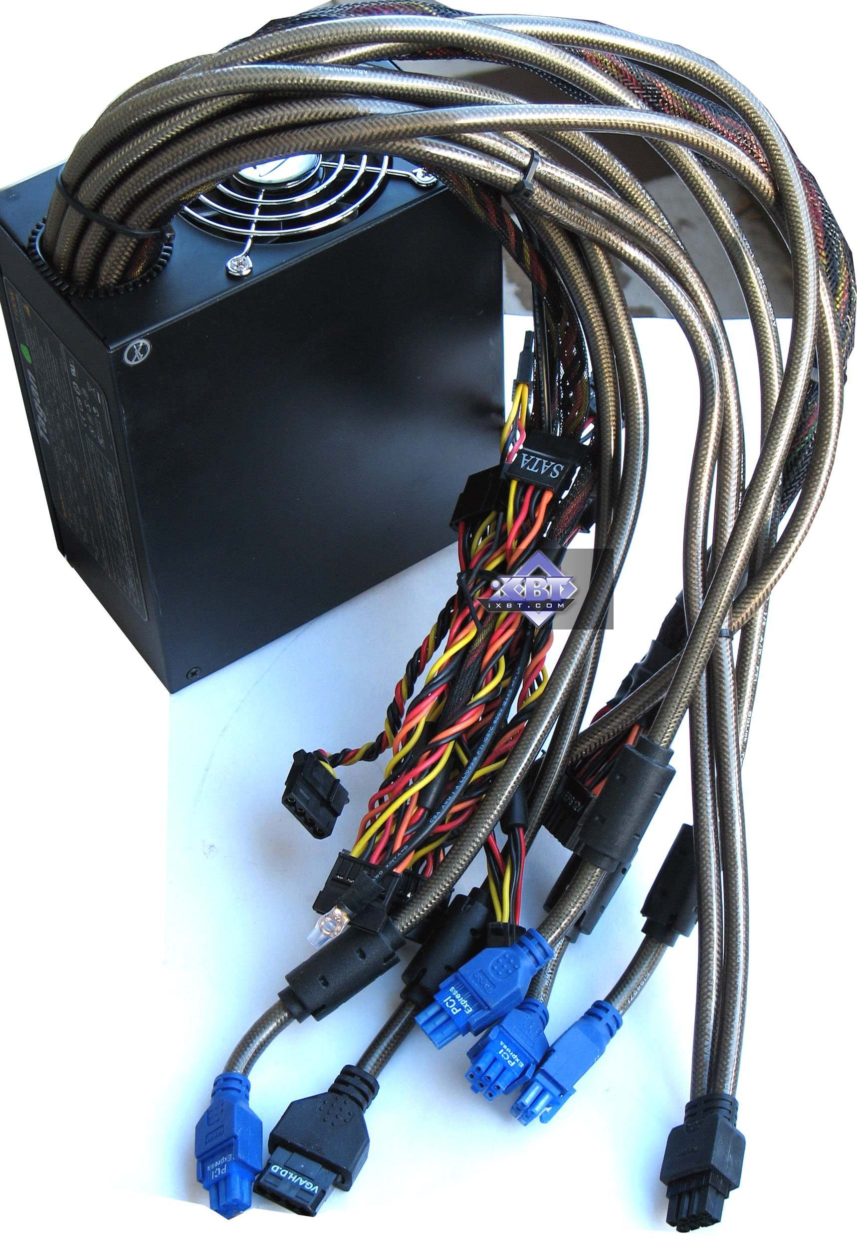 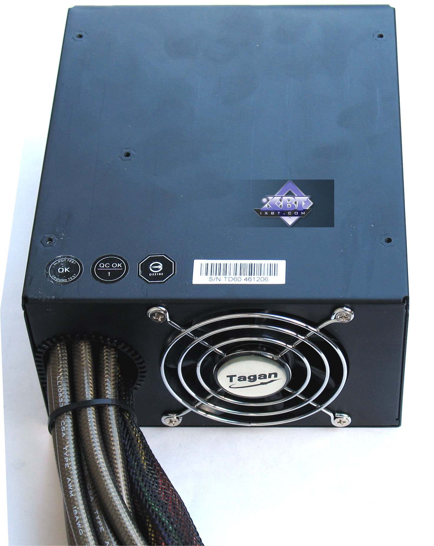 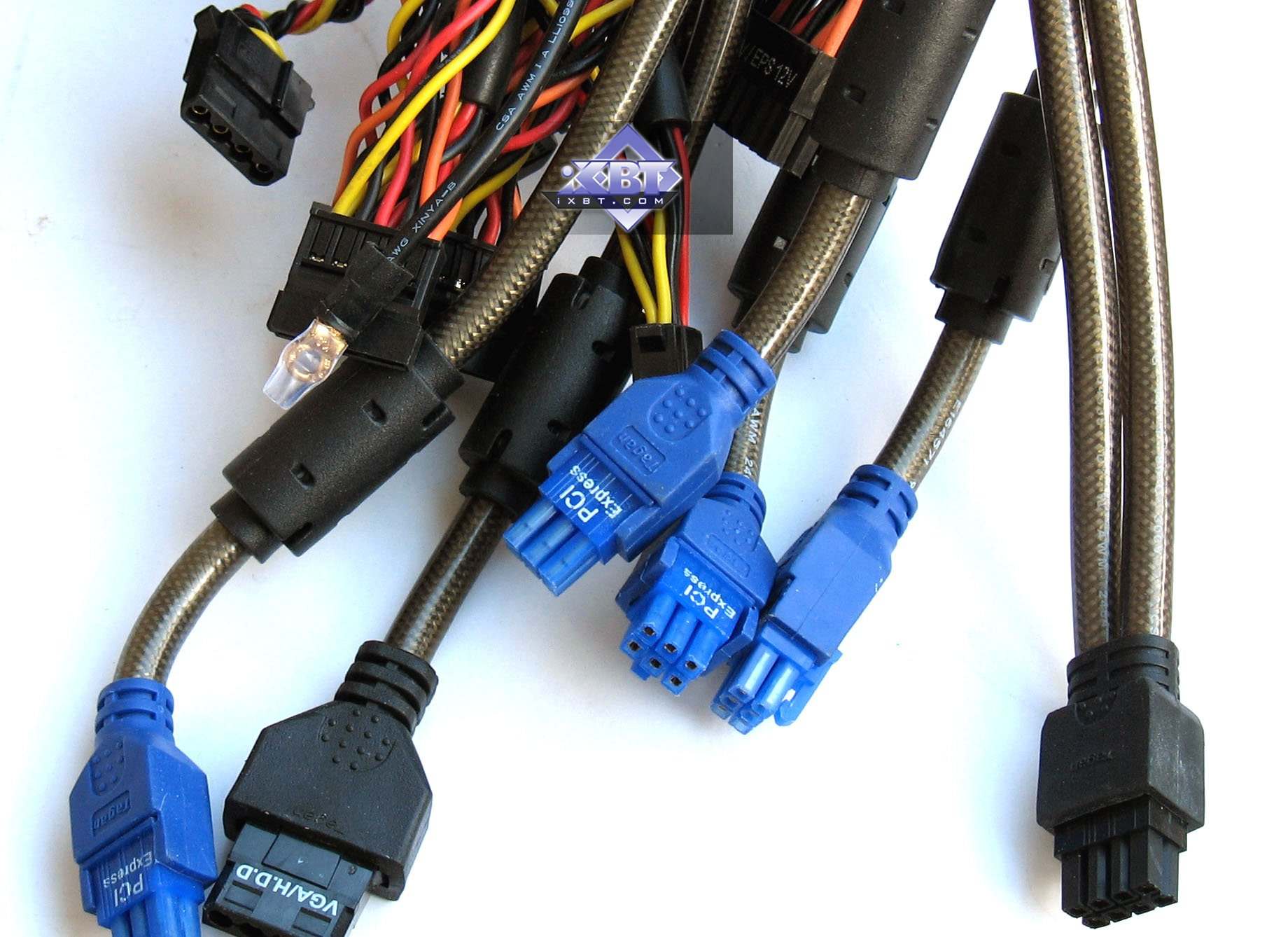 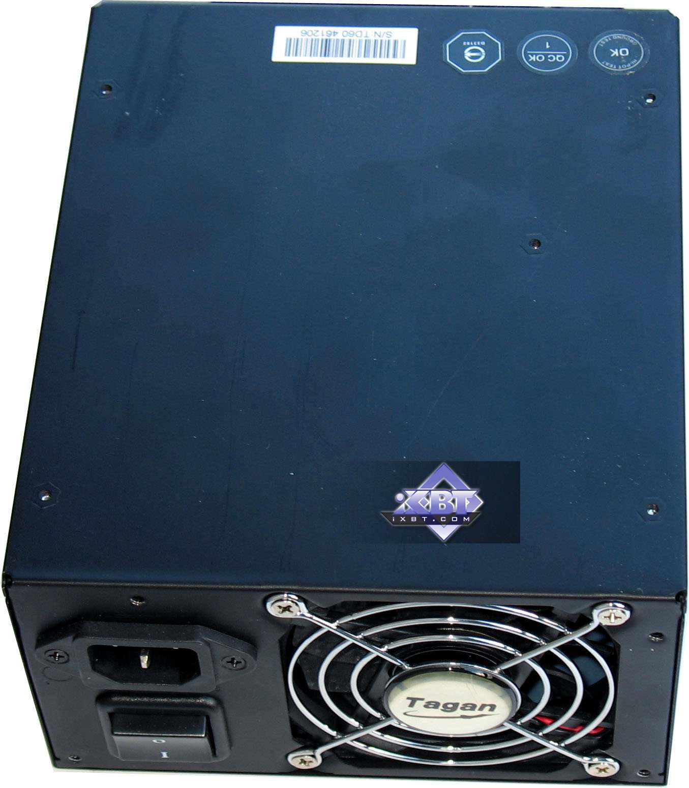 Full characteristics are specified on the PSU (look at the photo above), so there is no point in repeating them here. The PSU is equipped with FOUR (!) PCI-E slots (just enough to test 8800 GTX SLI!), it has all necessary power connectors (24-pin, 8-pin, 4-pin). But unfortunately, there is only one cable with Molex, while there are lots of cables for SATA. We should take into account lots of motherboards with additional requirements to Molex power. Besides, no one abolished optical devices with this connector. So you cannot do without additional Molex splitters. All cables are thoroughly screened, so the bunch of cables is very tight. PSU fans are very slow even when working with the above-mentioned testbed configuration and the GeForce 8800 GTX, so there is almost no noise. In case of the 8800 GTX SLI, the rotational speed grows, but the PSU is still not noisy. All in all, it's a good solution. It will even suffice for future upgrades.
Installation and DriversTestbed configuration:
VSync is disabled.
In fact, the latest RivaTuner beta, written by Alexei Nikolaychuk, already supports this accelerator.
NVIDIA GeForce 8800 GTX (G80) 768MB PCI-E
 The first screenshot shows the card working at standard frequencies. We can see that the maximum core temperature does not exceed the normal limit, the cooler remains quiet. The second screenshot shows the accelerator at increased frequencies. The card was cooled by a side fan, so maximum core temperature was a tad lower than in the previous case.
Synthetic tests
D3D RightMark Beta 4 (1050) and its description (used in our tests) are available at http://3d.rightmark.org
We also used new complex tests of pixel shaders 2.0, adequate to our tasks - D3D RightMark Pixel Shading 2 and D3D RightMark Pixel Shading 3, intended for future tests. These tests are in beta testing right now and are already available for downloadhere: Our contenders:
Pixel Filling test
Peak texelrate, FFP mode, various numbers of textures applied to a single pixel:
 We can see well that 32 texture units in the G80 offer much power. A wide memory bus provides enough ground to reveal their potential. Their efficiency is getting close to the theoretical maximum. It's also obvious that texture units work at the standard frequency, not at the doubled one like ALU. However, unlike short ALU pipes, a texture unit converting texture coordinates, sampling and filtering values is perhaps the most complex and the longest pipeline. If we compare the results with GX2 - both chips formally have 48 texture units (more), but their efficiency in synthetic tests is lower not only due to SLI overheads, but also because G80 units are significantly overhauled - they are noticeably more efficient. It can be the effect of unified chip architecture - for example, ALU G80 can be potentially used in this test for generating texture coordinates. Anyway, the new leader is evident, even doubled GX2 cannot catch up with it. Let's have a look at the rate of writing data into a frame buffer: 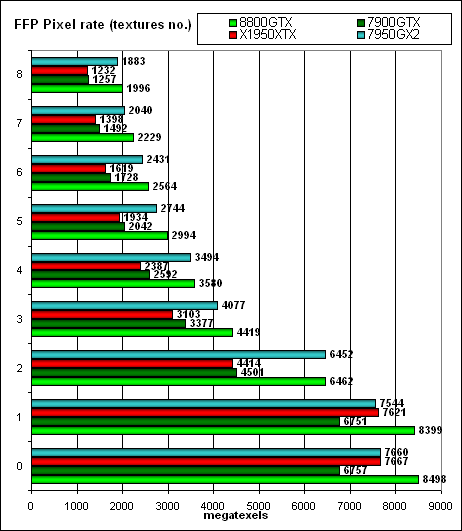 It's the same situation, but in terms of a number of pixels written into a frame buffer. In peak cases – 0, 1, and 2 textures - G80 takes up the lead.
Let's test the same task, but with PS 2.0:
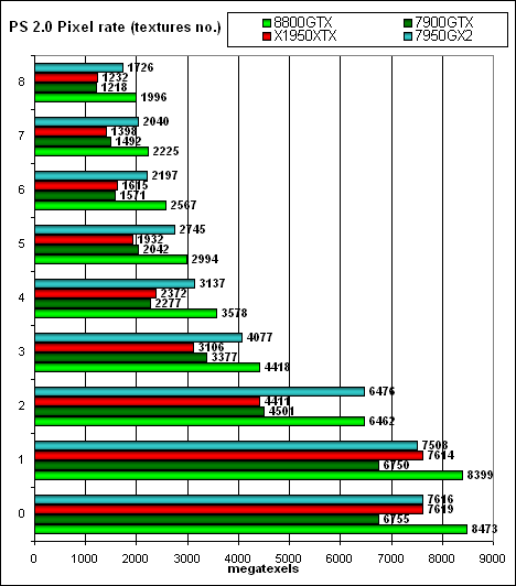 As we expected, nothing has changed — FFP as well as shaders operate in the same way (in terms of hardware FFP is emulated by shaders) and demonstrate the same results. Higher efficiency of G80 in this test allows this chip to dominate GX2. You should understand that synthetic tests in case of a unified architecture are like a razor - you should use them very carefully. Synthetic tests provide a lopsided load, while real applications will distribute GPU resources between different tasks. While the old chip can still demonstrate results close to the peak values (in a well balanced game), the unified chip in a complex application can noticeably slow down compared to its synthetic results. So it will be very interesting to compare our synthetic results with the situation in games (in the next part). Geometry Processing Speed test
The simplest shader — maximum bandwidth in terms of triangles:
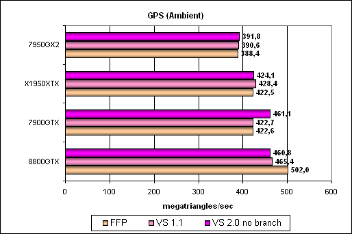
G80 leads here as well, but its advantage is not very large, as performance here is limited by API and the platform rather than by the accelerator. With the release of DX10 results of such peak tests may grow significantly.
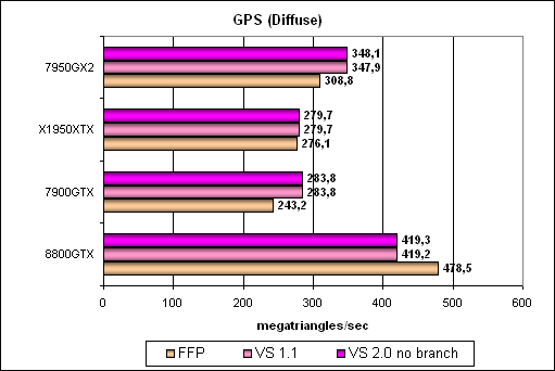
The tendencies are the same, but the differences are more pronounced here. Let's complicate the task:
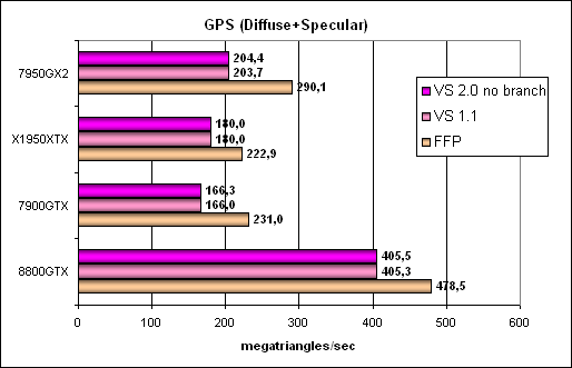 The situation has taken shape and the leader raises no doubts. Unified architecture has spread its wings, while SLI overheads did not let GX2 to demonstrate really doubled results. Optimized FFP emulation reveals itself in case of a mixed light source – it's demonstrated to this or that degree by all contenders. It's a more complex task that includes branching: 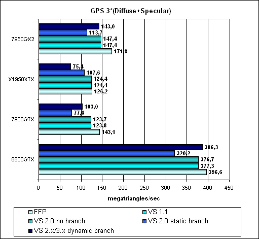 That's another proof of the evident fact - G80 architecture is the architecture of the future. The harder a task, the more flexible shaders, the better this chip performs, breaking further away from competitors of the previous generation. As usual, branching is a weak spot of ATI's vertex unit. Let's hope that R600 will be a truly unified chip in this respect and the situation will change. As in case of G7X, G80 prefers dynamic branches to static ones. Conclusions on geometry tests: G80 is an evident leader. Burdened with no SLI overheads and capable of directing all its 128 ALUs (operating at doubled frequency) to solve geometric tasks, this chip demonstrates excellent flexibility of the unified architecture and excellent capacities for working with complex dynamic code of vertex shaders. More that two-fold advantage - bravo! Let's see what awaits us in real applications. And we are looking forward to the release of DX10 that will help reveal full potential of this chip. Pixel Shaders Test
The first group of shaders, which is rather simple to execute in real time, 1.1, 1.4, and 2.0:
 To all appearances, these tests just don't let the G80 reveal its potential - they are too simple. GX2 demonstrates better results in the simplest tests, even the 7900GTX looks good versus G80. What's the matter? Performance is limited by API and the platform so far. Such shaders are a thing of the past for our chips under review.
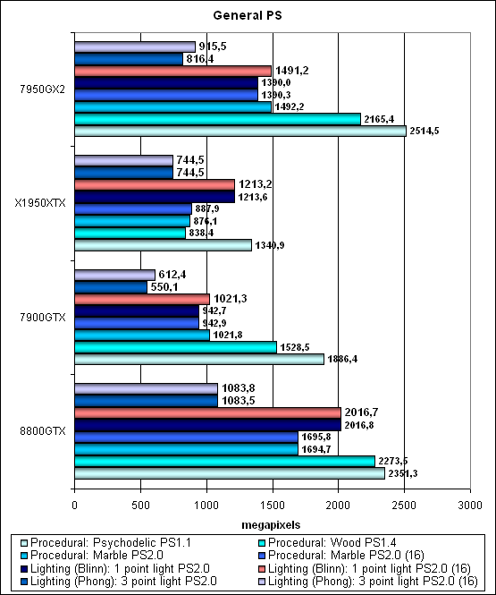
Let's look at longer shaders:
 Aha, here is food for thought. Firstly, the unified architecture of G80 DOES NOT depend on precision of calculations and storage of intermediate results. At last you don't have to save on quality - you can always use 32-bit floating point calculations that guarantee excellent results without any rounding artifacts. Like in case with ATI, the results are absolutely identical for any precision. Besides, GX2 slightly outperforms G80 in texturing-dependent Water test (48 versus 32 units and the total of 512-bit buses in SLI mode versus 348), we can even speak of parity. But G80 takes up the lead in a more computation-intensive lighting test. Excellent computational capacity, ALU, ALU, and again ALU :-). The layout of forces in pixel shaders can change in real applications, but general tendencies are already clear. . Our new shader testsThe new tests, to replace gradually our old tests in future reviews, can be downloaded (see above) as part of D3D RightMark beta. In future we are going to give up synthetic tests with old SM versions and focus on HLSL shaders for SM 2.0 and 3.0. Older shaders can be tested in real applications. And synthetic tests, developed for the present or even for the future, should be adjusted for modern requirements, which has been done. Let's start with simpler Shaders PS 2.0. We have two new tests with modern effects:
Both shaders are tested in two variants: oriented to computations and to texture sampling. Besides, we obtain results for FP16 and FP32.
So, computation-intensive variants:
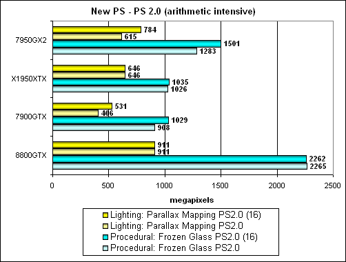
As we can see, G80 is always victorious (it's especially good at Frozen-Glass). GX2 noticeably lags behind due to SLI overheads and less flexible architecture. G80 performance does not depend on precision again. Now the same tests modified for texture sampling:
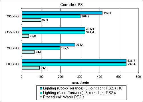
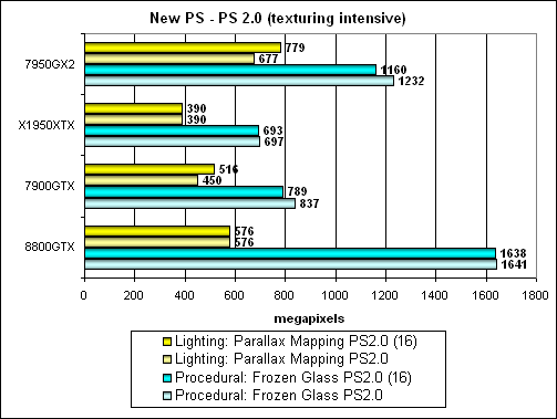 G80's advantage is less pronounced here, including absolute results. This chip certainly likes computations more than texturing. 32 texture units are necessary here. If the bus could be wider, there might have been 48 of them. But now GX2 leads in some tests. Too much depends on context and developers' preferences here. In order to reveal full potential of the G80, they will evidently have to choose (create) computation-intensive variants of their algorithms - in this case G80 will be able to gain 50% of performance. And now the most flexible test - PS3. The test contains intensive dynamic branches in pixel shaders:  We have no doubts as to what architecture is the most advanced now and the best at working with dynamic branches in pixel shaders. It's G80. The second place is taken by unified RADEON, followed by GX2 (even SLI is of little help here for the old non-unified architecture). Conclusions: Out of doubt, G80 is a new powerful computational architecture, well suited for executing the most complex pixel shaders. The more complex a task, the more computations it has, the larger is the gap between G80 and its competitors. In some cases programmers can get noticeable performance gains by optimizing their algorithms for computations instead of texture sampling. We can predict that there are some games, where the chip can gain advantage due to its 48 texture units and 512-bit memory bus. But the company makes a compromise here - it chooses flexibility and computational capacities for future applications. G80 is the model platform for shaders with dynamic branching. We'll see what DX10 will bring us. We'll also see how it will change the layout of forces in real applications, especially in modern and outdated ones. HSR test
Peak efficiency (with and without textures) depending on geometry complexity:

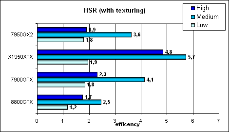 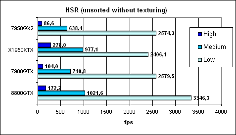
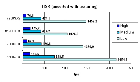 As we can see, there are no positive changes in the layout. Compared to NVIDIA's previous generation, it works better with complex scenes and worse with simple ones (i.e. it was slightly tuned to adjust to the modern situation). Hierarchical HSR from ATI still looks better than a single-level one from NVIDIA, especially in complex and medium scenes. While the G80's absolute results in texturing are still the best, the old chip from ATI still fares well in the most favorable mode for testing ATI cards (no texturing to burden 16 units, maximum scene complexity favors hierarchical HSR). But only in such artificial conditions. G80 takes the lead in real applications, even though its HSR itself is not the most efficient solution. Perhaps, it's a deliberate decision - NVIDIA engineers just used transistors to get higher yield in terms of real applications. The higher is drawing optimization of an application, the more noticeable is the general advantage of NVIDIA. Point Sprites test
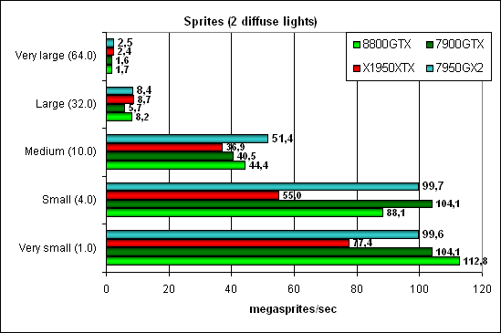 Everything is as usual – this test has been limited (in case of reasonable sprite sizes) by fill rate alone for a long time. GX2 and G80 are leaders here. Conclusions on the synthetic testsSo, the new top solution from NVIDIA, the new architecture, the new innovations. Everything is evident - synthetic test results confirm our theoretical assumptions. NVIDIA has designed a really flexible chip intended for complex dynamic shaders and computations. SLI of the previous generation is outperformed in many cases. To be more exact, G80 is beyond competition in shader tests. Potential problems are texture sampling and bus width, they are not always sufficient for such a computational monster. Well, NVIDIA has an obvious scope to get better in future. I wonder whether the situation in real applications will change (and how). Besides, we are looking forward to DX10 - to all appearances, only DX10 can reveal full potential of this chip in some spheres. NVIDIA did a great job from the architectural point of view. We have no doubts that this solution scales well both ways. So the company did the first step to lead in Middle End and future High End. I wonder what will be the response (R600). Will it be able to outperform G80, or it will reach only tardy parity. Read the most important section about gaming tests in the next part of the article. Stay with us! NVIDIA GeForce 8800 GTX (G80) - Part 3: Game Benchmarking Results And Quality Of Anisotropy
Write a comment below. No registration needed!
|
Platform · Video · Multimedia · Mobile · Other || About us & Privacy policy · Twitter · Facebook Copyright © Byrds Research & Publishing, Ltd., 1997–2011. All rights reserved. | |||||||||||||||||||||||||||||||||||||||||||||||||||||||||||||||||||||||||||||||||