 |
||
|
||
| ||
|
||
|
||
| ||
Today we are going to test low-level parameters is of the VIA C3 processors, in particular, desktop VIA C3 Ezra and mobile VIA C3 Antaur. Their performance was tested here, and now we will analyze the key features of these processors specified by VIA. Note that the documentation for C3 Ezra is much more detailed than that for Antaur. Specification of VIA C3 Ezra.
VIA says that C3 Ezra features large caches and TLB - they are greater than those of any other x86 CPU (which is wrong - just compare with the AMD K7/K8 platforms studied before). The additional details about this level of the Ezra microarchitecture cover the STLF (store-to-load forwarding) and WC (write-combining) buffers, each having four 8-byte entries (32 bytes). Finally, it supports the hidden speculative data prefetch in the D-Cache and the hidden aggressive instructions prefetch in the I-Cache. Later we will see whether they really work. Now comes the specification of the new VIA Antaur (it's very similar to Ezra):
There are few differences from Ezra. First of all, AMD's 3DNow! is replaced with Intel's SSE - a reasonable solution taking into account that the range of SSE optimized software solutions is much wider as compared to 3DNow!. Secondly, the 64KB L2 cache has a greater associativity (from 4 to 16) but unclear what for. Finally, the BTA cache further improves the traditional (for VIA) unique and complicated branch prediction mechanisms. That's all about the documentation. Testbed and softwareTestbed 1
Testbed 2 (MarcoPolo43T notebook)
Software
Real D-Cache/RAM BandwidthTraditionally, we start testing low-level parameters of the VIA C3 platforms with estimation of the real D-cache and RAM bandwidth. For that purpose we run the first RMMA test, Memory Bandwidth. The only possible extensions of the VIA C3 Ezra are MMX (3DNow! is not of much interest from the standpoint of the RAM bandwidth). That is why the L1/L2 and RAM bandwidth can be estimated on this platform only in one test - D-Cache/RAM Bandwidth, MMX Registers. 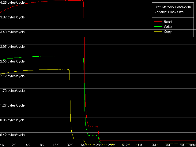 VIA C3 Ezra 733 MHz At the same time, the VIA C3 Antaur got SSE extensions, which allows us to estimate the d-cache and RAM bandwidth using both MMX and SSE registers. 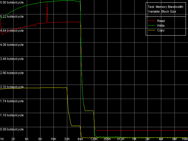 VIA C3 Antaur 1 GHz, MMX 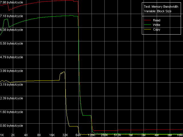 VIA C3 Antaur 1 GHz, SSE The diagrams show that both processors have a 64KB L1 cache, while the
effective size of the L2 cache is 128 KB. But this test doesn't define
whether the L2 cache is 128KB inclusive or 64KB exclusive. But VIA's documentation
and the following tests make us think that this is a 64KB one - VIA (or
rather Centaur) followed AMD, and this was a justified step. It could be
a wrong step to use half of the L2 cache for doubling L1 data if it were
a 128KB inclusive cache.
So, the L1/Registers bandwidth of the Ezra makes 4.25 bytes/clock at reading and 2.64 bytes/clock at writing. According to VIA, this CPU can fulfill one MMX instruction per clock, i.e. theoretically the L1/registers bandwidth must be limited by 8 bytes (64 bits)/clock. The effective RAM BW is underestimated - the L1 efficiency makes 53% at reading and 33% ar writing. Antaur shows pretty interesting results - the L1 efficiency is just a bit higher at reading MMX operands (4.89 bytes/clock, 61% of the theoretical limit) and much higher at writing (up to 5.80 bytes/clock, i.e. 72.5% of the theoretical limit). Note that writing of MMX values is more effective than their reading - it happens very seldom. The SSE registers improve the L1 cache BW a lot - it grows up to 7.98 bytes/clock at reading and up to 7.08 bytes/clock at writing. Unfortunately, we could find no information in the VIA Antaur specs about the speed of execution of SSE instructions, but it looks like that it takes 2 clocks for one simple SSE instruction. It makes the L1 cache access limit equal to MMX - 8 bytes/clock (half of the SSE operand is sent per clock). The L2 cache BW is, as usual, much lower. Ezra shows 0.61 bytes/clock at reading and 0.34 bytes/clock at writing. It has an immediate effect on the real RAM BW - 161.6MB/s at reading (15.2% of the limit) and 111.0MB/s at writing (10.4% of the limit). And a weak link in the chain is the L1-L2 bus. Its bandwidth in case of total data reading makes only 528MB/s at reading and 294MB/s at writing which is much lower than the theoretical RAM BW of the memory type used (1067MB/s). Taking into account such a lower L1-L2 bandwidth in case of total reading/writing it doesn't make sense to speak about VIA praised CPU features meant to minimize the FSB idle time. This parameter is much better in Antaur - the effective L2 BW is increased up to 1.28 bytes/clock (1280MB/s) in case of total reading/writing. But it's still too low taking into account that the chipset used supports PC2100 DDR the theoretical limit of which is 2133MB/s. As compared to Ezra, the real L2 BW is 110% higher at reading and 276% higher at writing. Undoubtedly, it affected the average/minimal L2 latency and the real L1-L2 bandwidth at writing/reading of cache lines which will be studied a bit later. Finally, the real RAM BW has also grown up to 433-439MB/s at reading (more than twice, which can't be explained by using DDR instead of SDRAM) and 151-200MB/s at writing (the higher values are reached with the SSE registers). Maximum RAM BandwidthIt's not that simple to estimate the maximum real RAM BW on Ezra. This processor doesn't have the extensions required (MMX Extensions) which are used in the RAM read/write optimization methods. That is why it's possible to measure only using the method of reading/writing cache lines (L2 to RAM and back) - it's a bit "dishonest" from the standpoint of the memory access optimization, because the respective RAM BW values can't be be reached using total reading/writing. But it can be used for estimation of the maximum real RAM BW because the memory is accessed at the level of the L2 whole lines the size of which equals 32 bytes for VIA C3 processors. On Ezra the real RAM BW at reading reached 227MB/s (only 21.3% of the limit but it's 40.5% higher compared to the total reading). The real RAM BW makes 205MB/s which is not much either (19.2% of the theoretical maximum), but it's 84.8% higher compared to the total reading from MMX registers. Although the C3 Ezra processors have the write-combining buffers we can't estimate the access speed because of lacking instructions of forward data writing from the CPU registers to the memory. At the same time, with the SSE Antaur has everything necessary for complete estimation of the memory access optimization. Since the test scores for the MMX and SSE modes do not differ at the qualitative level the pics will be shown only for the SSE registers. 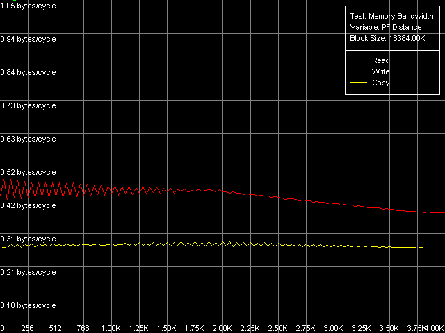 VIA C3 Antaur 1 GHz, SSE, Software Prefetch 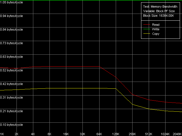 VIA C3 Antaur 1 GHz, SSE, Block Prefetch 1 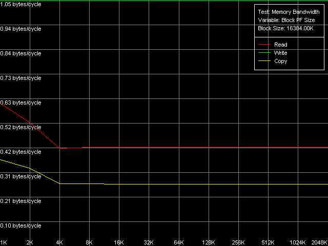 VIA C3 Antaur 1 GHz, SSE, Block Prefetch 2
*the parentheses contain the values calculated relative to the theoretical maximum bandwidth of a given memory type.The row of the optimizations at reading got one abnormal value - Maximal RAM Bandwidth, Software Prefetch, MMX Registers. 334.1MB/s is lower than the average RAM BW at reading (439.0MB/s). Probably it's just because the power saving mode was enabled, since the method of the Maximal RAM Bandwidth, Software Prefetch, SSE Registers shows pretty good scores - 484.7MB/s (22.7% of the limit, which is 11.8% over the average RAM BW). At the same time, it's far from the maximum yet. As you can see, the Block Prefetch methods allow for a higher RAM BW, like for AMD K7. Thus, the CPUs from VIA and AMD look similar, probably, because of the identical d-cache hierarchy. The Block Prefetch efficiency is higher with Block Prefetch 2 (specific for K8) as compared to Block Prefetch 1 (specific for K7), as well as with the SSE registers vs MMX. That is why the maximum RAM BW is reached in the method of Maximal RAM Bandwidth, Block Prefetch 2, SSE Registers and makes 609.0MB/s (28.6% of the limit). But it's not an absolute limit either. The limit can be reached at reading of the cache lines (D-Cache Bandwidth, L2 Cache-RAM Bus Bandwidth) and makes 660.4MB/s (31.0% of the limit). I must say that the maximum RAM BW reached on Antaur at reading is far from the theoretical maximum in all cases (only 1/3 of the bandwidth of this memory type is actually used).
*the parentheses contain the values calculated relative to the theoretical maximum RAM bandwidth.Let's have a look at the RAM writing optimization methods. The maximum (1046.3MB/s - 49.1% efficiency) is reached with the Non-Temporal store method, like for AMD K7/K8, Intel Pentium 4 and Intel Pentium III/Pentium M. At the same time the cache lines writing method doesn't allow for any considerable gain when accessing the memory because 200.4MB/s reached corresponds to the average value obtained in case of the total data writing from the SSE registers of Antaur (200.8MB/s). Let's have a look at the results obtained when measuring the real RAM BW as they look questionable for DDR. If the low maximum real RAM BW at reading can be explained by the narrow L1-L2 bus the real bandwidth of which in case of the total reading doesn't exceed 50% of the theoretical DDR RAM BW, the situation with data writing in the non-temporal store method is not that clear. VIA's "ultra efficient DDR memory controller" of the CLE266 chipset is not that good when handling DDR, right? It's quite possible. And it's possible that it handles this memory type as if it were SDRAM! (note that the memory controller of this chip is specified to support both DDR and SDRAM) D-Cache/RAM LatencyFirst we are going to estimate latency of various levels of the memory subsystem for Ezra and Antaur (D-Cache Latency, D-Cache/RAM Latency). 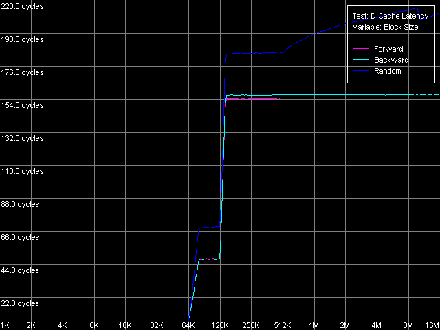 VIA C3 Ezra 866 MHz 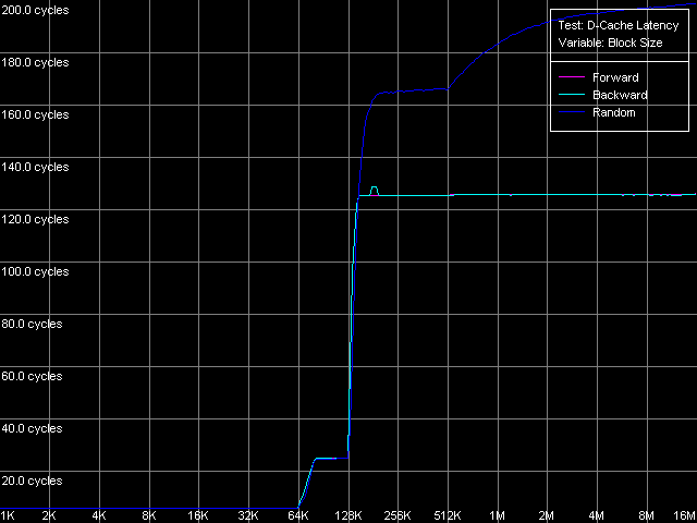 VIA C3 Antaur 1 GHz The random memory access latency gradually grows up when crossing the
512 KB mark. It grows up because the D-TLB buffer resources (the buffer
of translation of virtual memory pages into physical addresses) are exhausted,
its size must be equal to 128 entries (512 KB / 4 KB). Here are the figures.
* 4 MB block sizeThe L1 cache access latency is pretty high on Ezra - 4 clocks in all modes. Only the Intel Pentium 4 Prescott showed similar latency. Surprisingly, the L1 d-cache latency on Antaur is even greater - it reaches 6 clocks (!) - it's more than any other CPU tested has, though the bandwidth of this cache level is increased on Antaur. In contrast, the L2 latency looks pretty good for Antaur. It was expected as we know that the L1-L2 bus is wider in Antaur compared to Ezra. It's also interesting that the random latency is also pretty high on Ezra (69 clocks against 48 for forward/backward). It means that its L1-L2 bus works optimally only in the forward/backward access modes, while the random access causes additional delays. It seems that line eviction from L1 to L2 when a new line is loaded from L2 into L1 is not that good. Nevertheless, it works well in Antaur because its L2 latency in all access modes makes 25 clocks. The architectural improvements of Antaur have a positive effect on the RAM latency (126 ns) as compared to Ezra (180 ns) - it has fallen down by 30%. Although these platforms use different memory types, the DDR memory used on Antaur doesn't show its worth. The average random latency measured in case of the 4MB buffer is certainly much higher - 241 ns on Ezra and 195 ns on Antaur (a 20% gap). It can partly be explained by the fact that the D-TLB buffer is used up but the random latency of both processors within the area of 128-512 KB is also higher than the average forward/backward access latency. Minimal L2 D-Cache/RAM LatencyFirst we are going to estimate the minimal L2 cache latency. We will unload a respective data bus by inserting NOPs (Minimal L2 Latency, Method 1 preset). Note that automatic measurement of one NOP on these CPUs overestimated them (1.03 clocks on Antaur, 1.10 clocks on Ezra, against 1.00 clock), that is why the diagrams needed to be corrected. 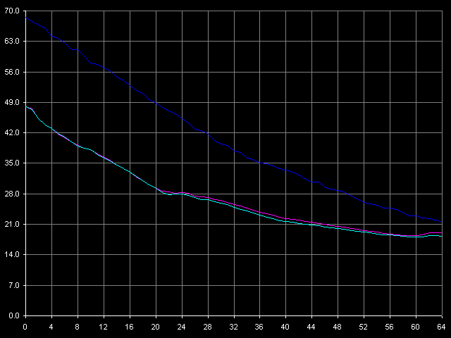 VIA C3 Ezra 866 MHz  VIA C3 Antaur 1 GHz The L2 latency on Ezra gradually falls down from the average values
to minimal, which make 17 clocks in all access modes (for the random access
it is reached at the number of NOPs over 64). On Antaur the minimal latency
is reached at 8 NOPs and makes 17 clocks as well. The difference between
the L1-L2 busses of Ezra and Antaur is well seen in this test. Although
the minimal latency coincides for both processors, the cost is different.
Ezra prefers very seldom L2 accesses (two accesses can be separated by
60-70 clocks) - only in this case the minimal latency of this cache level
can be reached. At the same time, if accesses are frequent (when they are
not separated) Ezra performs twice worse than Antaur.
*4MB block sizeNow we are going to measure the minimal RAM latency in case of a 4MB buffer, with the Minimal RAM Latency, 4 MB Block preset. The diagrams are also corrected taking into account the error in measuring one NOP duration.  VIA C3 Ezra 866 MHz  VIA C3 Antaur 1 GHz According to this test, an important fact about both C3 processors is that they lack the Hardware Prefetch algorithm, though the hidden speculative data loading is specified, because uploading of the L2-RAM bus doesn't make the memory access latency lower even in the forward mode. Instead, we can notice typical jagged curves in all access modes. The distance between the teeth for Ezra is equal to 6-7 clocks which corresponds to factor 6.5 (866.6 / 133.3 = 6.5). Antaur has it one clock higher (7-8 clocks), because one FSB clock corresponds to 7.5 CPU clocks for this processor (1000.0 / 133.3 = 7.5). The minimal RAM latency on Ezra is 166 ns on average (forward/backward), which is 7.8% lower than the average (180 ns). The minimal random latency in the same conditions - 236 ns - is only 2% lower than the average value (241 ns). At the same time, unloading of the L2-RAM bus on Antaur hardly makes any effect - the minimal forward/bckward latency is equal to the average value (126 ns), and the random one is 4 clocks lower than the average (192 ns). It means that Antaur's BIU and L1-L2 bus works more effectively than those of Ezra, even in case of more frequent memory accesses. D-Cache Associativity VIA C3 Ezra 866 MHz The fact is that Ezra's L2 cache doesn't reveal its specified associativity equal to 4. The chains 1-4 on the diagram correspond to the specified L1 associativity. At the same time, there's no second bend on the curve which for the exclusive cache architecture must be seen in the zone of the summary associativity of both cache levels (8 in this case). We can see it only in case of 5 chains, i.e. it looks like the L2 associativity is equal to 1.  VIA C3 Antaur 1 GHz As to Antaur, its L1 associativity turns out to be twice increased (8-way, against 4-way specified), while the 16-way L2 associativity specified doesn't show itself at all. What I can say is that the pseudo-LRU algorithm differs from that in Intel/AMD CPUs where we got more (AMD) or less (Intel) clear and interpretable associativity diagrams. Real L1-L2 Bus BandwidthD-Cache Bandwidth test, L1-L2 Cache Bus Bandwidth preset. 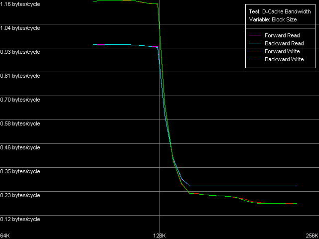 VIA C3 Ezra 866 MHz 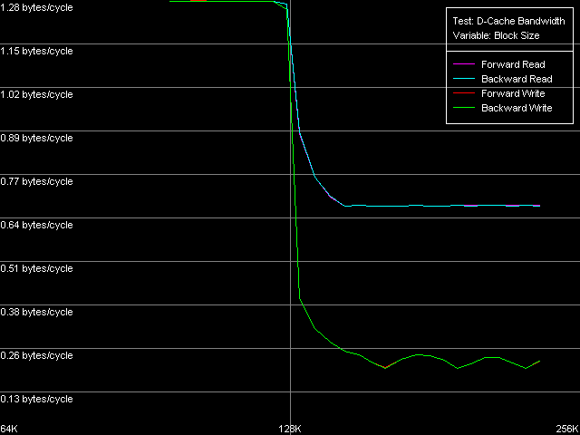 VIA C3 Antaur 1 GHz Since the VIA C3 processors have the exclusive cache architecture the
real L1-L2 bus measured in this test within the range of 64-128 KB must
be doubled since one operation of accessing the L2 cache transfers one
cache line (32 bytes) from L2 into L1 and simultaneously evicts the victim
line from L1 into L2.
*with the cache exclusive architecture taken into accountThe bandwidth of this bus is really low in case of Ezra - only 1.88 bytes/clock at reading and 2.32 bytes/clock at writing. Again, the write speed is higher than the read one. Antaur has 2.56 bytes/clock in both cases, which is higher than those of Ezra (by 36% at reading and by 10% at writing of cache lines). Such a low absolute real bandwidth of the L1-L2 bus could made us think that this bus has a low bit capacity - let's say 32 bits (up to 4.0 bytes/clock inclusive). But it's not so, the bus capacity must be at least 64 bits at reading. Let's carry out one more test called D-Cache Arrival,L1-L2 Cache Bus Data Arrival Test 1, 32 bytes.  VIA C3 Ezra 866 MHz  VIA C3 Antaur 1 GHz This test accesses twice the same cache line with the variable offset of the second line element (4-28 bytes) relative to the first one which is always located at the beginning of the line. You can see that the summary latency of two accesses in all access modes on Ezra and Antaur doesn't depend on the offset of the second element (up to 28 bytes inclusive). The overall latency of such access equals 21 CPU clocks for Ezra and 23 clocks for Antaur, which coincides with the overall L1 and L2 latency (17+4 and 17+6 clocks respectively). Lack of delays when accessing any element of the line requested means that it takes 4 clocks of accessing L1 on Ezra and 6 clocks of accessing L1 on Antaur from L2 to transfer a whole cache line of 32 bytes. It means that the theoretical L1-L2 bandwidth must be 32/4 = 8 bytes/clock for Ezra and 32/6 = 5.33 bytes/clock for Antaur at least. In both cases these values correspond to the 64-bit L1/L2 bus for VIA C3 processors. Trace Cache, decode efficiencyHere you can see the results of the I-Cache test carried out with L1i Size / Decode Bandwidth, CMP Instructions 3 preset which decodes and executes simple 6-bytes instructions cmp eax, 0x00000000. 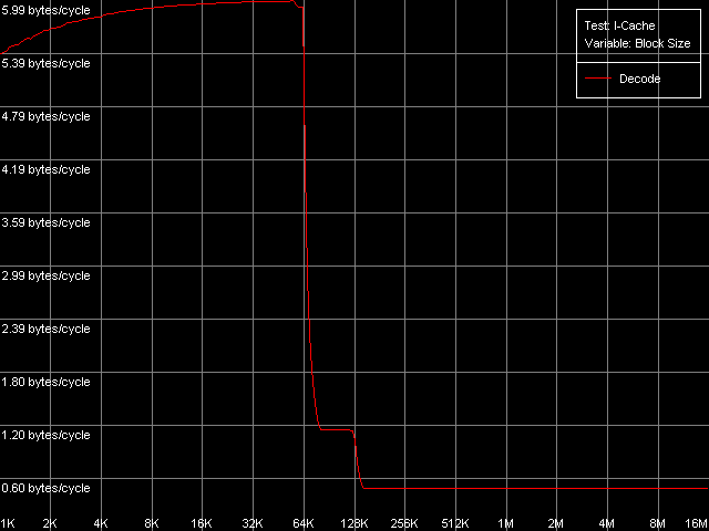 VIA C3 Ezra 866 MHz 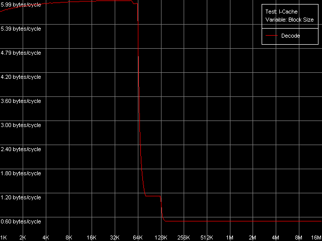 VIA C3 Antaur 1 GHz Note that exactly in this case we can achieve the maximum speed of decoding/execution of x86 ALU instructions by the VIA C3 CPUs - 6.0 bytes/clock, it corresponds to execution of one instruction per clock. Judging by these curves, the L1 instruction cache size is equal to 64 KB and the L2 cache is a unified data/instruction cache the size of which, with the exclusive organization taken into account, also makes 64 KB. The results obtained completely coincide with the VIA specs. Now we are going to test decoding/execution of other simple x86 ALU
instructions.
The speed of instruction decoding both from L1i and from L2 is identical for both processors. It means that the ALU decoder hardly changed in Antaur as compared to Ezra. The real limit of the decode efficiency is one instruction/clock which is probably set by the pipeline and execution units architecture of Ezra/Antaur. The analysis of Ezra's documentation shows that there's only one Integer ALU. The rate of execution of CMP 2 (cmp ax, 0x00) and Prefixed CMP 1-4 ([rep][addrovr]cmp eax, value) is lower. Comparing the number of prefixes used by these instructions and the rate of their execution we can see that the VIA C3 processors take every prefix as a separate instruction! In the first case (CMP 2) one prefix is used (operand-size override, 0x66), i.e. such instruction is considered by the C3 decoder as two instructions. That is why the rate of its execution is twice lower (1 instruciton/2 clocks). In the second case (Prefixed CMP 1-4) the decoder gets two prefixes with the cmp instruction, that is why its rate of execution is three time lower (1 instruction/ 3 clocks). Let's prove it with the Prefixed NOP Decode Efficiency test. 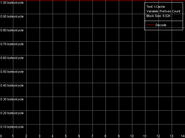 VIA C3 Ezra 866 MHz  VIA C3 Antaur 1 GHz So, the rate of execution of [0x66]nNOP instructions (in bytes/clock) doesn't depend on the number of prefixes (n = 0-14), that is why every prefix (including identical prefixes coming one after another) is executed as separate instructions. Well, VIA/Centaur take the problem of prefixes very simple - they don't use clipping like in Intel Pentium 4 processors. Now let's get back to efficiency of instruction decoding and look at the L2 cache values. Except the simple one-byte NOP (the rate of decoding/execution of which is limited by the CPU pipeline), the efficiency of instructions decoding from L2 makes 1.15 bytes/clock (0.58 instrucitons/clock and lower), which is obviously limited by the rate of loading of instruction from L2 into L1 which is carried out by the "aggressive" hidden algorithm :). By the way it doesn't look that ironic - 1.15 bytes/clock is really higher than data loading from L2 to L1 at the speed of 0.61 bytes/clock. Antaur has it different - data loading is quicker (1.28 bytes/clock) than swapping of instructions from the same cache into L1i. Instruction cache associativityAs we can see above, the attempt to measure d-cache associativity of Ezra/Antaur failed. Let's see whether the instruction cache of these processors will pass this test. I-Cache Associativity preset. 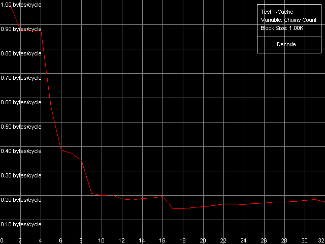 VIA C3 Ezra 866 MHz 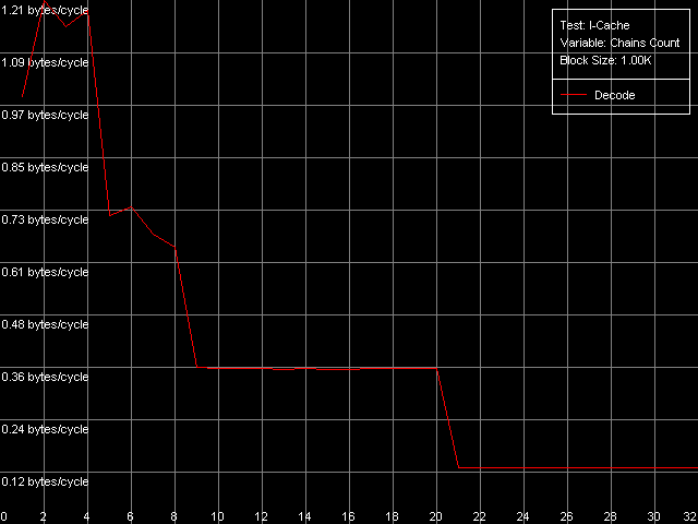 VIA C3 Antaur 1 GHz The instruction cache of Ezra/Antaur shows an adequate associativity picture. The chains 1-4 for both processors corresponds to the L1i cache with the associativity equal to 4. The second zone in case of Ezra covers 5-8 chains and corresponds to the L1i+L2 associativity equal to 8 because both caches have associativity equal to 4. The respective zone on Antaur covers 5-20 chains because the L2 associativity of this processor was increased up to 16, and the summary L1i+L2 associativity is thus equal to 20. It's not clear why the unified L2 cache performs so strangely in the d-cache associativity tests and adequately in the i-cache associativity. D-TLB parametersThere's one surprise waiting for you here - this time only from Ezra. Just have a look at the diagrams obtained in the D-TLB test, D-TLB Size preset. 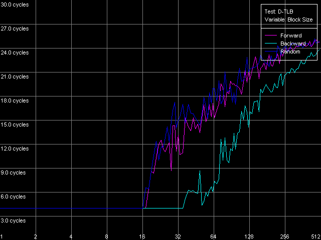 VIA C3 Ezra 866 MHz 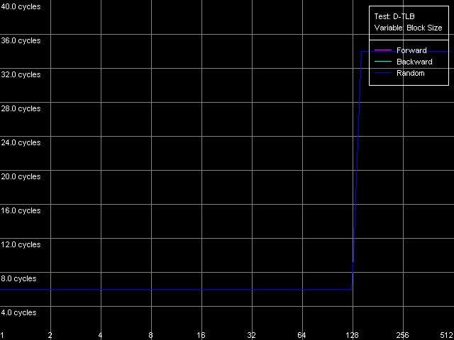 VIA C3 Antaur 1 GHz As we mentioned above, the D-TLB size of both processors must be 128 entries. And Antaur proves it. But Ezra draws beautiful curves! They indicate that the D-TLB size of the latter is only 16 entries. We can also see that the D-TLB miss is too expensive for Antaur - the L1 latency reaches 34 clocks. In case of Ezra the miss is less expensive - the L1 latency grows up to 24 clocks. Let's also measure the D-TLB associativity of the processors. D-TLB Associativity, 16 Entries preset for Ezra selected and their number is decreased to 8. 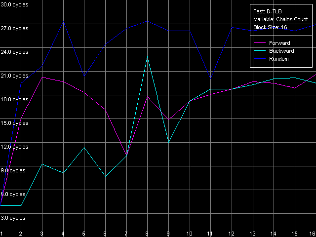 VIA C3 Ezra 866 MHz Well, we can see that the defective D-TLB of Ezra contains 16 entries and have the associativity equal to 1! The documented values of these parameters are 128 entries of pages and the associativity level equal to 8. The first is proved in the latency test, but the latter can't be measured using indirect methods. At the same time, the curves for Antaur, in D-TLB Associativity, 64 Entries preset, look much more logical. 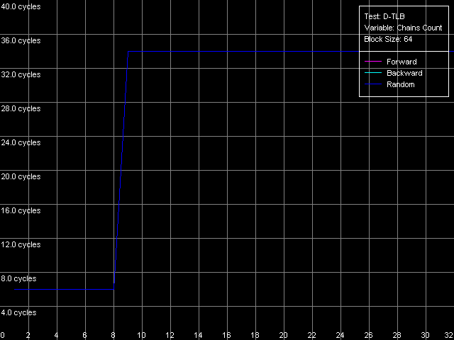 VIA C3 Antaur 1 GHz They coincide (i.e. all D-TLB modes show identical results) and allow defining the D-TLB associativity correctly (8). Besides, the D-TLB miss, at the expense of its associativity "breakdown", is followed by the same increase in L1 latency - up to 34 clocks, like a simple buffer overstep. I-TLB featuresThe I-TLB tests do not look surprising at all. They have completely expectable results, plus they uncover some additional peculiarities of realization of the Ezra/Antaur architecture. So, let's look at the curves in the I-TLB test, I-TLB Size preset. 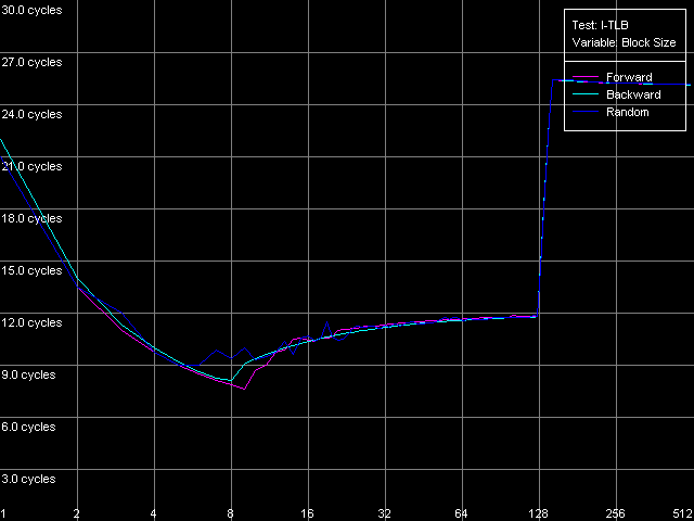 VIA C3 Ezra 866 MHz 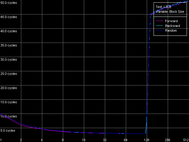 VIA C3 Antaur 1 GHz The I-TLB size of both processors is evidently equal to 128 entries. This test actually measures latency of execution of a series of operations of unconditional jumps (mov ecx, addr_val; jmp ecx). In the zone of a small number of pages where the I-TLB size is sufficient the leader is Antaur - the latency of execution of such combination of instructions is within 3-5 CPU clocks, against 9-12 clocks of Ezra. Antaur thus has a better branch prediction algorithm than Ezra (probably because of the BTA cache). At the same time, the I-TLB miss is much more expensive for Antaur (45-50 clocks latency) than for Ezra (25-26 clocks latency). The I-TLB associativity is pretty clear. Just look at the diagrams obtained with the I-TLB Associativity, 64 Entries preset. 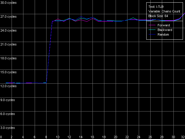 VIA C3 Ezra 866 MHz 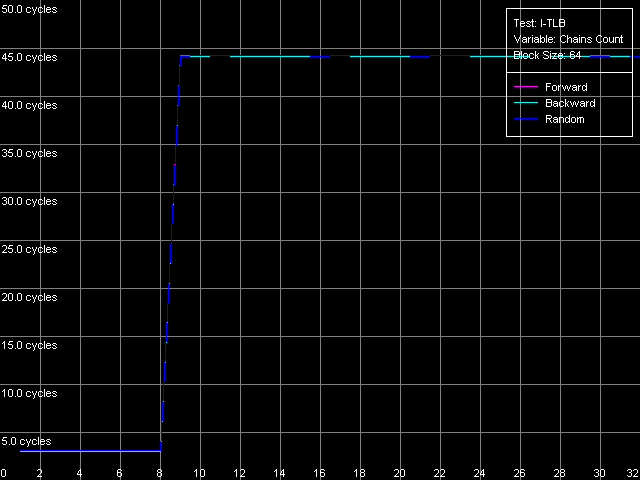 VIA C3 Antaur 1 GHz In both cases the I-TLB associativity is equal to 8 (as specified), and its "breakdown" causes the increase in latency of execution of jumps over the memory (up to 25-26 clocks for Ezra and approximately up to 44 clocks for Antaur), like the buffer overstep. ConclusionThe low-level tests of the VIA C3 Ezra/Antaur platforms prove that they
are really fully x86 software compatible processors. No transcoding of
instructions is used - all instruction are executed correctly, judging
by the I-Cache test results. It's hard to say how the 3DNow! in Ezra was
replaced with SSE in Antaur. It's probable that the execution units of
the CPU remain the same but the SSE instructions are transferred via the
same 3DNow! unit, that is why it takes at least two clocks (it can be also
a reason why the pipeline architecture is hidden). The most important improvement
of the VIA Antaur microarchitecture is the much improved L1-L2 exclusive
cache bus which made a positive effect on its bandwidth and the L2 latency,
which were bottlenecks for VIA's C3 Ezra. Finally, I must say that these
CPUs show strange results when measuring associativity of the data cache
and D-TLB size/associativity of Ezra.
|
Platform · Video · Multimedia · Mobile · Other || About us & Privacy policy · Twitter · Facebook Copyright © Byrds Research & Publishing, Ltd., 1997–2011. All rights reserved. | ||||||||||||||||||||||||||||||||||||||||||||||||||||||||||||||||||||||||||||||||||||||||||||||||||||||||||||||||||||


