 |
||
|
||
| ||
|
||
|
||
| ||
AMD And IBM Detail Early Results Using Immersion And Ultra Low-k In 45nm Chips Cooler Master Rolls Out CM Media 280 HTPC DFI Unveils LANParty UT ICFX3200-T2R/G Motherboard On RD600 Chipset NEC and NEC Electronics Develop World's First 32nm-Node Multi-Layer Interconnect Sharp Develops Basic Technology for RRAM, Next-Gen Nonvolatile Memory IBM, Macronix & Qimonda Show New Memory Chip Technology SanDisk And Sony Develop 'Memory Stick PRO-HG' Format Abit Introduces PCI-E Wi-Fi Card AMD And IBM Detail Early Results Using Immersion And Ultra Low-k In 45nm Chips At the International Electron Device Meeting (IEDM) today, IBM and AMD presented papers describing the use of immersion lithography, ultra-low-k interconnect dielectrics, and multiple enhanced transistor strain techniques for application to the 45nm microprocessor process generation. AMD and IBM expect the first 45nm products using immersion lithography and ultra-low-K interconnect dielectrics to be available in mid-2008. Current process technology uses conventional lithography, which has significant limitations in defining microprocessor designs beyond the 65nm process technology generation. Immersion lithography uses a transparent liquid to fill the space between the projection lens of the step-and-repeat lithography system and the wafer that contains hundreds of microprocessors. This significant advance in lithography provides increased depth of focus and improved image fidelity that can improve chip-level performance and manufacturing efficiency. In addition, the use of porous, ultra-low-K dielectrics to reduce interconnect capacitance and wiring delay is a critical step in further improving microprocessor performance as well as lowering power dissipation. This advance is enabled through the development of an ultra-low-k process integration that reduces the dielectric constant of the interconnect dielectric while maintaining the mechanical strength. The addition of ultra-low-k interconnect provides a 15 per cent reduction in wiring-related delay as compared to conventional low-K dielectrics. The continued enhancement of AMD and IBM's transistor strain techniques has enabled the continued scaling of transistor performance while overcoming industry-wide, geometry-related scaling issues associated with migrating to 45nm process technologies. In spite of the increased packing density of the 45nm generation transistors, IBM and AMD have demonstrated an 80 percent increase in p-channel transistor drive current and a 24 per cent increase in n-channel transistor drive current compared to unstrained transistors. This achievement results in the highest CMOS performance reported to date in a 45nm process technology. Source: AMD
Cooler Master Rolls Out CM Media 280 HTPC Cooler Master introduced the new CM Media 280, with its roomy interior capable of supporting NVIDIA SLI / ATI Crossfire Configuration and capacity to hold up to five HDDs. It is also compatible with RAID configuration. The spacious dimensions allow you to have full-length cards, including the NVIDIA G80 SLI. According to the press release, the most unique mechanical design on CM Media 280 is the two front bezels of the case. They can be removed easily to convert from a desktop to a tower case. You have the freedom to choose which style fits your needs and is best suited for your lifestyle. The thick aluminum plates include VFD and hot key module, which are automatically configured with XPs built-in drivers and its Microsoft Window Vista Ready. Features:
Source: TechMessenger
DFI Unveils LANParty UT ICFX3200-T2R/G Motherboard On RD600 Chipset The merger of ATI and AMD placed the RD600 chipset in an unusual position. Despite that DFI decided to continue production plans for the RD600. The power of the chipset's graphics processing capabilities with the incorporation of physics processing support has drawn interest from every hardcore gamer and over-clocking enthusiast around the world. The release of the LP UT ICFX3200-T2R/G combines power of ATI's chipset with support for the latest Intel CPUs, such as the Core 2 Extreme/Quad/Duo, it may very well be the grand finale of the ATI/Intel partnership but will not be forgotten. The press release claims that the performance of RD600 will easily surpass all previous ATI chipsets in every respect including overclockability, processing power and graphics quality. The LANParty UT ICFX3200-T2R/G supports all of Intel's latest Core 2 Extreme/Quad/Duo series processors using the ATI RD600 chip for the Northbridge and utilizing the SB600 for the Southbridge. 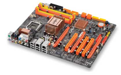 The new motherboard provides users with 3 sets of PCI Express x16 slots. Two of the slots are used for ATI Dual x8 Crossfire processing while the other PCIe slot (the 3rd slot) provides PCIe x2 for the physics rendering card. When a CPU is overclocked it not only requires more power but also demands a more stable power supply. For this reason the DFI engineers have built a Six Phase Digital PWM on the DFI LANParty UT ICFX3200-T2R/G to ensure that the power that the CPU receives is always stable. This power supply design allows users to rest assured that they will never experience "blowouts" and that the CPU will be provided with clean currents up to 200A ensuring that the extra load from CPU overclocking is completely met. The new LANParty UT ICFX3200-T2R/G motherboard supports voltage adjustments for the memory, Northbridge, HT, Southbridge as well as the CPU core. The wide range of BIOS options allows users to fine-tune the board. To maximize its overclocking potential the DFI LANParty UT ICFX3200-T2R/G motherboard is equipped with four DDR2 slots. Support is provided for single or double sided DDR2-800 and DDR2-1066 memory and also allows the memory voltage to be raised up to 3.2V. DFI's new LANParty UT ICFX3200-T2R/G motherboard is also provided with two Teaming technology equipped GbE LAN interfaces controlled by the high-performance Marvell 88E9052 GbE PCI-E and Marvell 88E8053 GbE PCI-E chips. The novelty offers a total of 8 SATA interfaces. The Southbridge chip controls 4 of the SATA-2 interfaces enabling the setup of RAID 0, RAID 1 or RAID 0+1 arrays; the other 4 SATA-2 interfaces are controlled by a Promise PDC40719 chipset that supports RAID 0, RAID 1, RAID 0+1 and RAID 5. For audio, the Karajan audio module returns once more in the DFI LANParty UT ICFX3200-T2/G motherboard. It uses the RealTek ALC885 8CH sound decoder chip certified by Microsoft as Windows Vista Premium Ready. Source: DFI
NEC and NEC Electronics Develop World's First 32nm-Node Multi-Layer Interconnect NEC Corporation and NEC Electronics Corporation today announced that they have successfully developed the world's first multi-layer interconnect for 32nm-node LSIs. The joint research verified the excellent performance and high reliability of the new interconnect, owing to a newly developed low-k dielectric technology based on a plasma co-polymerization technique. In advanced LSIs, the number of interconnects between transistors increases, while the amount of space between interconnects decreases due to miniaturization. This trend leads to higher inter-line parasitic capacitance, which may cause longer signal delays. The introduction of porous low-k dielectrics such as molecular pore stacking film is one solution to minimizing parasitic capacitance. However, existing porous low-k technologies cannot provide sufficient mechanical strength and insulation reliability at the 32nm-node and beyond. NEC and NEC Electronics have developed a technology that overcomes these issues, while simultaneously ensuring the high performance and low power consumption needed for next generation network servers and mobile terminals. Features of the new technology
As the integration density of Si LSI devices increases, the number of interconnects increases, resulting in higher parasitic capacitance and undesirable power consumption levels. One approach to decreasing parasitic capacitance is the introduction of low-k films such as organic silica films (SiOCH) with low polarizability, which have already been introduced in 90nm-node LSIs. Porous low-k films (obtained by introducing pores into low-k films) have been investigated for 65nm-node LSIs to further decrease capacitance. By further advancing low-k material technology, NEC, in collaboration with the MIRAI project, developed a molecular-pore-stack (MPS) low-k film, in which sub-nanometer pores were introduced uniformly. This film was then successfully applied to 45nm-node LSI interconnects. However, there was still a challenge that needed to be addressed before 32nm-node interconnects could be realized. In general, porous low-k films are effective in decreasing parasitic capacitance, but their mechanical strength tends to decline as the porosity increases. Therefore, porous low-k films are usually used in combination with films possessing high mechanical strength. With conventional technology, these films are deposited with different processing tools, but changing tools while the film is grown inevitably exposes the wafer surface to the air, causing residual defects between each film, and giving rise to nonideality in the insulation property. NEC and NEC Electronics' new technology achieves consecutive formation of different types of films in a single step, with a single tool, without breaking the vacuum. The density modulation technology for low-k films enables control of dielectric constants and mechanical strength of low-k films by changing the mixing ratio of two types of precursors using plasma co-polymerization technology. This single-step deposition prevents creation of defects at the interface between films, resulting in a decrease in leakage current by three orders of magnitude as compared with conventional interconnects. Moreover, the mechanical strength of the new film is twice as strong as that of conventional film, while maintaining an equal dielectric constant. Simultaneously, a novel, selective, dry-etching technique with enhanced precision was developed. This technique allows sensitive detection of the density modulation of low-k films. By combining the above achievements, a highly reliable low-k interconnect structure was realized that does not incur current leakage, despite miniaturization of the patterning dimensions down to 50nm for 32nm-node LSIs. Moreover, interline capacitance of 83fF/mm was accomplished; a level in line with that previously achieved for 45nm-node interconnects, proving successful in suppressing power consumption. In 32nm-node ULSI interconnects, integration density is equivalent to that of placing a maximum of ten thousand lines within 1mm-width. NEC and NEC Electronics will present the results of this research at the International Electron Devices Meeting (IEDM) 2006, being held from December 11 - 13 in San Francisco, USA. Source: NEC Corporation
Sharp Develops Basic Technology for RRAM, Next-Gen Nonvolatile Memory Sharp Corporation has developed basic technology for a novel high-speed programming system for RRAM (Resistance Random Access Memory), a next-generation nonvolatile memory capable of programming data at rates about 100 times faster than flash memory. Based on collaborative research with the National Institute of Advanced Industrial Science and Technology, an independent administrative agency of the Japanese government, these results are the first step toward the practical use of this memory technology. Further R&D, including IC integration and microfabrication technologies, will continue in the future aimed at bringing a commercially viable product to market. RRAM is a memory device in which electrical resistance changes of a metal oxide film are functioned as the stored information, and this device can be operated with low voltages and at high speeds. There are high expectations for RRAM to be a next-generation memory that will enable large amounts of data to be programmed into memory at high speeds with low power consumption. However, it is not yet clear how resistance changes work in the metal oxide film, the key component of RRAM, and achieving a memory device that takes full advantage of the outstanding characteristics of RRAM has proven difficult. In collaborative research with the National Institute of Advanced Industrial Science and Technology, Sharp has focused on resistor constituents other than the resistor components where the information of the RRAM memory devices is stored. The resistor constituents, which had not previously been controlled, were set to the different values when data is programmed and erased. As a result, the company has achieved a High-Speed Unipolar Switching. Programming and erasing RRAM had previously required a positive and a negative power source, but this Sharp development makes these operations possible using a single power supply. The result is memory elements that function using simple circuit architecture. Dramatically simplifying the cell structure of the RRAM, which can program data at high-speeds and low power consumption, makes it possible to reduce the cell size. This technology also uses materials that are highly compatible with conventional CMOS processes, allowing existing production lines to be used. Source: Sharp Corporation
OCZ Technology 600W EvoStream Modular SLI Power Supply Review @ Bigbruin Antec Nine Hundred Ultimate Gamer case review @ DH BFG GeForce 8800 GTS @ TrustedReviews ASUS EAX1950PRO 256MB @ Techgage OCZ Summit 2006 APAC - Memory, Motherboards and More Overclocking Goodness @ HWZ OCZ 2GB PC6400 Special Ops Edition Urban Elite Review @ Madshrimps Apevia X-Cruiser @ techPowerUp Installing Windows Vista For N00bs Posted! @ Tech ARP Creative Zen Nano Plus 1GB review @ DVHardware HEXUS Dragon Tour 2006 :: Latest articles Mod of the Year 2006 at bit-tech Sytrin KuFormula SHF1 Hard Drive Cooler @ Bjorn3D Thermaltake Toughpower 850w Modular Power Supply Review @ Tweaknews.net Technic3D / Gigabyte GA-M59SLI-S5 Mainboard Review Futurelooks News Flash - Holiday 2006 - Things You Can Buy a Computer Gamer That They'll Keep XTracPads Ripper XXL reviewed @ BurnOutPC Legion Hardware - (CPU Scaling With The GeForce 8800 GTX) Video: Jabra BT325S Bluetooth Headset @ Digital Trends AOA Forums Review: A look at aftermarket chipset cooling ATP 512MB 3-in-1 microSD Combo Flash Drive Review @ The TechZone Mushkin XP2-5300 Dual Channel DDR2 Kit @ MadBoxPC Casio EX-Z1000 10MP Digital Camera @ BonaFideReviews Gainward BLISS 7950 GT 512MB Golden Sample Review @ MVKTech Beginners Guides: Windows XP Safe Mode Explained @ PCSTATS Targus 17" XL Notebook Backpack @ GideonTech IBM, Macronix & Qimonda Show New Memory Chip Technology Scientists from IBM, Macronix and Qimonda announced joint research results that give a major boost to a new type of computer memory with the potential to be the successor to flash memory chips, which are widely used in computers and consumer electronics like digital cameras and portable music players. The advancement heralds future success for "phase-change" memory, which appears to be much faster and can be scaled to dimensions smaller than flash enabling future generations of high-density "non-volatile" memory devices as well as more powerful electronics. Non-volatile memories do not require electrical power to retain their information. By combining non-volatility with good performance and reliability, this phase-change technology may also enable a path toward a universal memory for mobile applications. 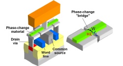 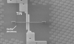 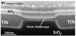 Working together at IBM Research labs on both U.S. coasts, the scientists designed, built and demonstrated a prototype phase-change memory device that switched more than 500 times faster than flash while using less than one-half the power to write data into a cell. The device's cross-section is a minuscule 3 by 20 nanometers in size, far smaller than flash can be built today and equivalent to the industry's chip-making capabilities targeted for 2015. This new result shows that unlike flash, phase-change memory technology can improve as it gets smaller with Moore's Law advancements. The new material is a complex semiconductor alloy created in an exhaustive search conducted at IBM's Almaden Research Center in San Jose, Calif. It was designed with the help of mathematical simulations specifically for use in phase-change memory cells. The technical details of this research will be presented this week at the IEEE's 2006 International Electron Devices Meeting (IEDM) in San Francisco. Source: IBM
SanDisk And Sony Develop 'Memory Stick PRO-HG' Format
Memory Stick PRO-HG media format uses an enhanced, 8-bit parallel interface in addition to a conventional serial and 4-bit parallel interface. The interface clock frequency also increases to 60MHz from 40MHz. This means that maximum data transfer speed increases up to 480Mbps, or 60MB/s (theoretical value), three times as fast as that of Memory Stick PRO media. The minimum write speed at 8-bit parallel transfer is 120 Mbps, or 15MB/s. Since Memory Stick PRO-HG is an extended format of the Memory Stick PRO format, Memory Stick PRO-HG compliant host devices support the conventional Memory Stick PRO media as well as Memory Stick PRO-HG media. In addition, the Memory Stick PRO-HG media can be used conventional Memory Stick PRO compliant host devices as well as Memory Stick PRO-HG compliant host devices. Licensing for the development of Memory Stick PRO-HG compliant host devices is scheduled to commence in January 2007. The Memory Stick PRO-HG Duo media will be made available in 2007. Specifications:
Source: SanDisk
Abit Introduces PCI-E Wi-Fi Card abit introduced its new Wi-Fi solution - the AirPace Wi-Fi card, IEEE 802.11b/g WLAN device with PCI-E interface. In addition to the common client mode, software Access Point capability is also supported. The added software Access Point function allows other networked PCs and laptops to not only use storage and data on your computer but also take advantage of its connected peripherals such as printers or Internet access. 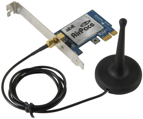 Specs:
Source: abit
Write a comment below. No registration needed!
|
Platform · Video · Multimedia · Mobile · Other || About us & Privacy policy · Twitter · Facebook Copyright © Byrds Research & Publishing, Ltd., 1997–2011. All rights reserved. |


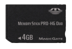 SanDisk Corporation and Sony Corporation announced the development of the Memory Stick PRO-HG format expanded from the Memory Stick PRO format.


