RV770 architecture
When engineers designed the new GPU, their main objective was to increase its efficiency. The task was to achieve two-fold advantage in theoretical performance versus the prev-gen GPU - RV670. In the light of the latest tendencies, it was also very important to improve GPU features in the field of non-graphics computing. Besides, it was the first time when they tried GDDR5 memory and crossed the psychological barrier of one teraflop (computing performance). NVIDIA almost reached it with its GT200.
The RV770 architecture combines several solutions from the previous R6xx architecture, but it has been significantly overhauled to improve its performance and efficiency. Let's have a look at the chart of the new GPU:
We can see a lot of changes in the RV770 architecture in comparison with the architecture used in the R600 and RV670, both quantitative and qualitative. Many bottlenecks were removed. But let's be consistent and examine the changes one by one...
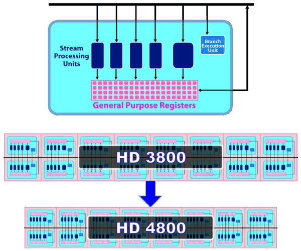
The main part of the RV770 chip consists of ten SIMD cores, each one containing 16 blocks of superscalar streaming processors, 160 all in all. The superscalar nature of these processors hasn't changed since RV670. So we can say that the GPU contains 160*5=800 scalar 32-bit streaming processors. The same units are used for 64-bit computations of double precision, only the computing rate drops.
The chip also includes other modifications: TMUs were modified and their number was increased, faster ROPs, cardinally changed memory/cache architecture, support for GDDR5, and other changes to raise the speed of executing geometry shaders and parallel non-graphics computations.
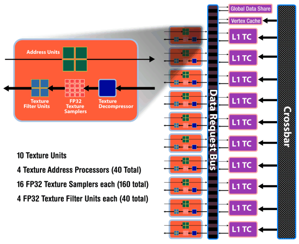
As we have already mentioned, each of ten SIMD cores contains 16 superscalar streaming processors (or 80 scalar ones), 16 KB of local memory to store data, and an individual dispatch processor. Besides, unlike R6x0 and RV670, TMUs are tied to a SIMD. Each of them has four dedicated texture units and L1 texture cache. The SIMD cores can exchange data using 16 KB of global memory. As we can see, the power of texture units in the new GPU is scaled together with the number of shader processors. ALUs relate to TMUs as 4:1.
Streaming processors haven't changed since RV670, but their density has been increased (the picture is a scaled version). So the number of streaming processors was increased to 800 with the same fabrication process. More aggressive clock gating is used to raise energy efficiency. It allows to disable logic units to reduce power consumption.
Besides, the superscalar design of streaming processors allowed AMD to implement support for double precision computing (FP64) using the same units in a more effective, easier way. As a result, RV770 offers much higher performance here, even though GT200 features special SPs for FP64 computations. The theoretical peak reaches 240 gigaflops.
Texture units have been significantly overhauled. Now they are tied to SIMD, and their efficiency is improved. Engineers removed the dedicated TMU pool, available in previous generations. So the current solution is similar to what NVIDIA did with TMUs, included into SIMD cores.
It's now impossible to fetch data without filtering, which could be done with vertex data. Texels and vertices are fetched by the same units in the new GPU, just like in the G8x and higher. On the other hand, each of 40 texture units in the RV770 is a tad weaker than each of 16 units in RV670. But there are more of them, and they operate at higher frequencies, so they should provide significant texturing performance gains.
Write a comment below. No registration needed!


