 |
||
|
||
| ||
|
||
|
||
| ||
Specifications of R[V]4XX and some RV3XX GPUs
Specifications of reference cards based on R[V]4XX and RV3XX
Details: R420, RADEON X800 SeriesR420 Specifications
R420 Flow Chart
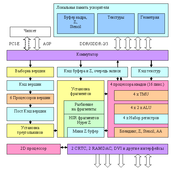 An attentive reader will notice right away that this flow chart is almost a complete match to NV40. There is nothing surprising about it - both companies try to design an optimal solution. Several generations have already used the time-proven and effective organization of the graphics pipeline general structure. Significant differences are hidden inside the units, in pixel and vertex processors in the first place. Like NV40, it has six vertex processors and four independent pixel processors, each of them working with one quad (2x2 pixel fragment). Unlike NV40, there is probably only one texture caching level. There are four independent quad processors that can be disabled. Thus, the manufacturer can lock one, two, or even three processors, depending on market demands and defective chips, to produce video cards processing 4, 8, 12, or 16 pixel per clock. And now we'll traditionally examine the most interesting places in more detail: Vertex processors and samplingHere is the flow chart of the R420 vertex processor:
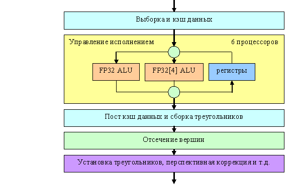 The processor itself is indicated by a yellow rectangle, the other units are shown to make the picture complete. The R420 is declared to have 6 independent processors (visualize the yellow unit copied six times). Vertex units comply neither with full VS 3.0 specifications (no texture access and dynamic branching) nor with Extended Specifications 2.0 as NVIDIA understands them (so called VS 2.0.a, which implies support for predicates and dynamic branches.) What concerns arithmetic performance - like an NV40 vertex processor, a vertex processor in the R420 can execute one vector operation (up to four FP32 components) and one scalar FP32 operation simultaneously per clock. Here is a summary table with parameters of vertex processors in modern accelerators from the point of view of vertex shaders in DirectX 9 API:
Another interesting aspect, which is analyzed in our reviews, is FFP (T&L) emulation performance. Remember that the R3XX was outperformed by NVIDIA chips in many respects due to the lack of special hardware units for calculating lighting, which had been accelerated T&L emulation in three generations of NVIDIA chips. Pixel processors and the fill processLet's analyze the pixel architecture of the R420 in the order of the data flow. That's what we get after setting up triangle parameters:  We'll dwell on the most interesting facts. Firstly, while R3XX used to have two quad processors maximum, which processed a block of four pixels (2x2) per clock, there are currently four such processors. They are completely independent, each of them can be excluded from operation (for example, to create a light version of a chip with three processors, if one of them is not effective). Note that this flow chart resembles that of the NV40 in many respects, but there are also cardinal differences, which we shall examine in more detail. So, at first a triangle is divided into units of the first level (8x8 or 4x4 depending on a rendering resolution) and the first stage of culling invisible units takes place based on the data in the integrated mini Z buffer. Its size is not published, but to all appearances it's a tad less than 200 KB in the R420. Up to four units can be culled per clock at this stage, that is up to 256 invisible pixels. Then follows the second division stage - this time into 2x2 quads. Completely occluded quads are culled based on the L2 Z Buffer (2x2 granularity) stored in video memory. Depending on MSAA mode, one element of this buffer may correspond to 4 (no), 8 (MSAA 2x), 16 (MSAA 4x), or even 24 (6x MSAA) pixels in a frame buffer. Hence it's detached into a separate structure, taking up an intermediate level between the on-chip mini Z buffer and the final Z buffer of the base level. Thus, NVIDIA products have the bi-level hierarchy of HSR and Z buffer, while ATI products offer three levels in their hierarchy. Then quads are set and distributed among active pixel processors. Now about the most important differences between R420 and NV40: Algorithm of NVIDIA's pixel processor: Cycle of shader commands
End of shader command cycle Algorithm of ATI's pixel processor
Cycle of four phases
End of cycle of the four phases. So, NVIDIA gradually executes commands (to be more exact, superscalar batches of commands, including texture sampling commands), driving all the quads to be processed through each command. ATI divides a shader into four phases (hence the limitation on the depth of dependent samples not to exceed 4), each of them starts with sampling all textures necessary for this phase and then follow calculations over the data obtained. Including calculations of new coordinates for texture sampling in the next phase. Which approach is better? We cannot say for sure. ATI's approach is ill-suited to complex shaders with instruction flow control or multiple dependent samples. On the other hand, calculations within each of the four stages are performed in the similar to CPU way - all instructions are executed one-by-one for one quad, then the next quad is processed, etc. Thus, unlike the NV40, we can use a sterling pool of temporal registers without any performance loss or penalty for using over four registers during calculations. Besides, ATI's approach requires few stages in a pipeline. Consequently, it results in fewer transistors spent and potentially higher clocks reached (or, in other words, higher yield of effective chips at the fixed clock). Shader performance is easily predictable. It's easier to program, when you don't have to take care of the even grouping of texture and math commands or the expenditure of temporal registers. Among the disadvantages are numerous limitations. Limitation on a number of dependent samples, limitation on a number of commands in one phase, requirement to store the entire microcode of the shader for the four phases "at hand", that is right in the pixel processor. Potential latencies in case of intensive successive dependent texture sampling (it's made less evident by a set of simultaneously processed quads, but their number is not as big as in NVIDIA.) In fact, ATI's approach is optimal for Shaders 2.0, without dynamic flow control and with seriously limited code length. Any attempts to add an unlimited shader length and especially unlimited flexibility of texture sampling to this pixel architecture inevitably run against problems. The flow chart of the pixel processor depicts the F-buffer mechanics - writing and restoring parameters of temporal shader variables. This trick allows to execute shaders that exceed the pixel processor limits as far as length or a number of dependent (as well as regular) texture samples are concerned, at the cost of additional passes. It's not a "free of charge" solution and is far from ideal. As a shader grows more complex, the number of passes and the volume of data stored temporarily in video memory will grow as well. It will be accompanied by growing penalties compared to NVIDIA-like architectures, which are not limited by the length or complexity of shaders But let's get back to architectural peculiarities of pixel processors in R420. Processors handle data in FP24 format. But operations with texture addresses, when a TMU samples textures, are performed with higher precision. There are two ALUs here per pixel, like in R3XX. Each ALU can execute two different operations (3+1 scheme like in R3XX, but that GPU has only one ALU). You can read about it in DX Current. Arbitrary masking and post-operational component rearrangement are not supported, only within Shaders 2.0 and a tad longer Shaders 2.0.b. Thus, depending on shader code, the GPU can execute from one to four different FP24 operations per clock over vectors (dimensionality up to 3) and scalars, plus a single access to the data, which has been already sampled from a texture in this phase. Performance of this tandem directly depends on a compiler and code. But we obviously have
The peak variant exceeds the NV40 capacities. But let's not forget that this solution is actually less flexible (always the 3+1 scheme) from the point of view of combining commands into superscalar batches during compilation. Computing efficiency of new pipelines has grown twofold in comparison with R3XX. Besides, there are twice as many of them. As they operate at higher frequency, this GPU has an advantage over the previous generation. All new improvements, such as longer shaders and new registers, are available in new Shaders 2.0.b. Let's have a look at the summary table of various shader features:
Let's return to the flow chart of pixel processors. Pay attention to the bottom part. You can see there units responsible for comparing and modifying color, transparency, Z, and Stencil values as well as MSAA. Unlike NV40 being able to generate up to 4x MSAA samples based on a single pixel, R420 generates up to 6. Like in NV40, productivity of computing Z and stencil values is doubled versus the base fill rate - 32 values per clock. Correspondingly, 2x MSAA suffers no penalty in performance, while 4x and 6x take up 2 and 3 clocks. However, this penalty is not noticeable and does not play an important role any more in case of pixel shaders at least several commands long. Memory bandwidth becomes more important. Of course, both color and Z values are compressed in MSAA modes. In the optimal case, compression ratio reaches the number of MSAA samples, that is it reaches 6:1 in MSAA 6x mode. Unlike NV40 that uses RGMS (rotated sample grid), R420 (like all R3XX chips) supports pseudo stochastic MSAA patterns on base 8x8 grid. As a result, antialiasing quality of edges and inclined lines in maximum modes is objectively higher. New drivers offer the so called Temporal AA. It consists in changing patterns from frame to frame. Thus, if your eyes or an inert LCD monitor has no problems with averaging neighboring frames (no excessive flickering), the antialiasing quality will be improved, as if we used more MSAA samples. There is no performance drop, but its effect may vary depending on a monitor and a frame refresh rate in an application. Technological Innovations in the R420Here are two main innovations in R4XX versus R3XX (the increased number of temporal registers and longer shaders in the pixel processor are evolutional rather than revolutional changes):
Details: RV410, RADEON X700 seriesRV410 Specifications
Specifications of the Reference RADEON X700XT
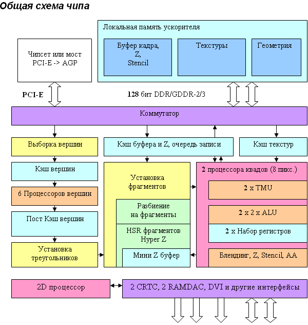 As we can see, there are no special architectural differences from R420, which is not surprising - RV410 is a scaled (fewer vertex and pixel processors and memory controller channels) solution based on the R420 architecture. The situation here resembles the one with NV40/NV43. Architecture principles of both competitors are similar in this generation. What concerns the differences between RV410 and R420, they are quantitative (bold elements on the diagram) but not qualitative - from the architectural point of view the chip remains practically unchanged. Thus, we have six vertex processors (like in R420, they may come in handy in some applications that are limited by geometry performance) and two (instead of four units in R420) independent pixel processors, each working with one quad (2x2 pixel fragment). PCI Express has become a native on-chip bus interface as in case with NV43. AGP 8x cards are equipped with an additional PCI-E -> AGP bridge (it's shown on the diagram). Architecture of vertex and pixel processors as well as of the video processor remained the same — these elements were described in detail in the review of RADEON X800 XT. And now let's talk about potential tactical considerations as to what was cut down and why. To all appearances, vertex and pixel processors in RV410 remained the same, but the internal caches could have been reduced, at least proportionally to the number of pipelines. However, the number of transistors does not give cause for trouble. Considering not so large cache sizes, it would be more reasonable to leave them as they were (as in NV43), thus compensating for the noticeable scarcity of memory passband). All techniques for sparing memory bandwidth were preserved - Z buffer and frame buffer compression, Early Z with an on-chip Hierarchical Z, etc. Interestingly, unlike NV43, which can do blending and write no more than 4 resulting pixels per clock, pixel pipelines in RV410 completely correspond to R420 in this respect. In case of simple shaders with a single texture, RV410 must get almost a twofold advantage in fillrate. Unlike NVIDIA, having a large ALU array (in terms of transistors) responsible for post processing, verification, Z generation, and pixel blending in floating point format, RV410 possesses modest combinators, and that's why their number was not cut down so much. However, the narrower memory bandwidth will not allow to write 3.8 full gigapixel per second in most cases anyway. The idea to retain all six active vertex units is no less interesting. On one hand, it's a strong point for DCC applications. On the other hand, we know that much depends on OpenGL drivers, a traditional strong point of NVIDIA solutions. Reference Information on RADEON R[V]4XX Graphics Cards Reference Information on RADEON R[V]5XX Graphics Cards Reference Information on RADEON R[V]6XX Graphics Cards Write a comment below. No registration needed!
|
Platform · Video · Multimedia · Mobile · Other || About us & Privacy policy · Twitter · Facebook Copyright © Byrds Research & Publishing, Ltd., 1997–2011. All rights reserved. | |||||||||||||||||||||||||||||||||||||||||||||||||||||||||||||||||||||||||||||||||||||||||||||||||||||||||||||||||||||||||||||||||||||||||||||||||||||||||||||||||||||||||||||||||||||||||||||||||||||||||||||||||||||||||||||||||||||||||||||||||||||||||||||||||||||||||||||||||||||||||||||||||||||||||||||||||||||||||||||||||||||||||||||||||||||||||||||||||||||||||||||||||||||||||||||||||||||||||||||||||||||||||||||||||||||||||||||||||||||||||||||||||||||||||||||||||||||||||||||||||||||||||||||||||||||||||||||||||||||||||||||||||||||||||||||||||||||||||||||||||||||||||||||||||||||||||||||||||||||||||||||||||||||||||||||||||||||||||||||||||||||||||||||||||


