iXBT Labs - Computer Hardware in Detail

Platform

Video

Multimedia

Mobile

Other

AMD(ATI) RADEON Graphics Cards


Reference Information on RADEON R[V]4XX Graphics Cards
Reference Information on RADEON R[V]5XX Graphics Cards
Reference Information on RADEON R[V]6XX Graphics Cards

R[V]5XX Specifications

Code name R580+ R580 R520 RV570 RV560 RV530 RV515
Baseline Article here here here here here here
Fabrication Process (nm) 90 80 90
Transistors (M) 384 321 330 330 157 105
Pixel Processors 48 16 36 24 12 4
Texture Units 16 12 8 4
Blending Units 16 12 8 4
Vertex Processors 8 5 2
Memory Bus 256 128
Memory Types DDR, DDR2,
GDDR3, GDDR4
DDR, DDR2, GDDR3
System Bus PCI-Express 16x
RAMDAC 2 × 400 MHz
Interfaces TV-Out
TV-In (a video capture chip is required)
2 × DVI Dual Link
Vertex Shaders 3.0
Pixel Shaders 3.0
Precision of pixel calculations FP32
Precision of vertex calculations FP32
Texture component formats FP32, FP16 (without filtering)
I8
DXTC*, S3TC
3Dc
Rendering formats FP32 and FP16 (the latter includes blending and MSAA)
I8
I10 (RGBA 10:10:10:2)
MRT available
Antialiasing 2x, 4x, and 6x MSAA
Pseudo random arrangement of samples on the 12x12 grid
Z generation 1x in Z-only mode, 2x in MSAA mode
Stencil buffer Double-sided
Shadow technologies No special technologies


Specifications of reference cards based on R[V]5XX GPUs

card chip
bus
PS/TMU/VS units Core clock (MHz) Memory frequency (MHz) Memory capacity (MB) Memory bandwidth (GB)
bit
Texel rate (Mtex) Fill
rate (Mpix)
RADEON X1300 (HM) RV515
PEG16x
4/4/2 450 500(1000) 32-128 GDDR3 4.0-16.0
(32/64/128)
1800
RADEON X1300 RV515
PEG16x/AGP
4/4/2 450 250(500) 128/256 DDR2 4.0-8.0
(64/128)
1800
RADEON X1300 PRO RV515
PEG16x/AGP
4/4/2 600 400(800) 256 DDR2 12.8
(128)
2400
RADEON X1300 XT RV530
PEG16x
12/4/5 500 390(780) 128/256 DDR2 12.5
(128)
2000
RADEON X1600 PRO RV530
PEG16x/AGP
12/4/5 500 390(780) 128/256 DDR2 12.5
(128)
2000
RADEON X1600 XT RV530
PEG16x/AGP
12/4/5 590 690(1380) 128/256 GDDR3 22.0
(128)
2360
RADEON X1650 PRO RV530
PEG16x
12/4/5 590 690(1380) 128/256 GDDR3 22.0
(128)
2360
RADEON X1650 XT RV560
PEG16x
24/8/8 600 700(1400) 256 GDDR3 22.4
(128)
4800
RADEON X1800 XL R520
PEG16x
16/16/8 500 500(1000) 256 GDDR3 32.0
(256)
8000
RADEON X1800 XT R520
PEG16x
16/16/8 625 750(1500) 256/512 GDDR3 48.0
(256)
10000
RADEON X1800 XT CFE R520
PEG16x
16/16/8 625 720(1440) 512 GDDR3 46.0
(256)
10000
RADEON X1900 GT R580
PEG16x
36/12/8 575 600(1200) 256 GDDR3 38.4
(256)
6900
RADEON X1900 XT R580
PEG16x
48/16/8 625 725(1450) 512 GDDR3 46.4
(256)
10000
RADEON X1900 XTX R580
PEG16x
48/16/8 650 775(1550) 512 GDDR3 49.6
(256)
10400
RADEON X1900 CFE R580
PEG16x
48/16/8 625 725(1450) 512 GDDR3 46.4
(256)
10000
RADEON X1950 PRO RV570
PEG16x
36/12/8 580 700(1400) 256 GDDR3 44.8
(256)
6960
RADEON X1950 XTX R580+
PEG16x
48/16/8 650 1000(2000) 512 GDDR4 64.0
(256)
10400
RADEON X1950 CFE R580+
PEG16x
48/16/8 650 1000(2000) 512 GDDR4 64.0
(256)
10400
card
chip
bus
PS/TMU/VS units
Core clock (MHz) Memory frequency (MHz) Memory capacity (MB) Memory bandwidth (GB)
bit
Texel rate (Mtex) Fill
rate (Mpix)


Details: R520, RADEON X1800

R520 Specifications

  • Codename: R520
  • Fabrication Process: 90 nm
  • 321 million transistors
  • FP¡ package (flip-chip, flipped chip without a metal cap)
  • 256 bit memory interface
  • Up to 1 GB of GDDR3 memory
  • PCI-Express x16 bus interface
  • 16 pixel processors
  • 16 texture units
  • Calculating, blending, and writing up to 16 full (color, depth, stencil buffer) pixels per clock
  • 8 vertex processors
  • FP32 processing throughout the pipeline (vertices and pixels)
  • Full SM 3.0 support, vertex texture fetch is not supported!
  • Efficient implementation of jumps and dynamic branches in pixel and vertex processors
  • Support for FP16 format: full support for data output into a frame buffer in FP16 format (including any blending and MSAA operations). FP16 texture compression, including 3Dc
  • The new integer data type, RGBA (10:10:10:2), for a frame buffer, for higher-quality rendering without FP16
  • New high-quality algorithm for anisotropic filtering (a user is given a choice between a faster or higher-quality anisotropy options), improved trilinear filtering
  • Support for a two-sided stencil buffer
  • MRT (Multiple Render Targets — rendering into several buffers)
  • Memory controller with a 512-bit ring bus, two alternate 256-bit rings (4 memory channels, programmable arbitration)
  • Efficient caching and a new more effective HyperZ implementation
  • 2 × RAMDAC 400 MHz
  • 2 × DVI interfaces supporting HDCP as well as HDMI via an adapter
  • TV-Out and TV-In, HDTV-Out
  • Video processor (for video compression, decompression, and post processing), a new generation that can accelerate operations with H.264 — a new algorithm for video compression used in HD-DVD and Blu-Ray video discs
  • 2D accelerator supporting all GDI+ functions
  • ATI CrossFire support

Details: RV530, RADEON X1600

RV530 Specifications

  • Codename: RV530
  • Fabrication Process: 90 nm
  • 157 million transistors
  • FP¡ package (flip-chip, flipped chip without a metal cap)
  • 128 bit memory interface (optional 64 bit configuration)
  • Up to 512 MB of DDR1/2 or GDDR3 memory
  • PCI-Express x16 bus interface
  • 12 pixel processors
  • 4 texture units
  • Calculating, blending, and writing up to 4 full (color, depth, stencil buffer) pixels per clock
  • 5 vertex processors
  • FP32 processing throughout the pipeline (vertices and pixels)
  • Full SM 3.0 support, vertex texture fetch is not supported!
  • Efficient implementation of jumps and dynamic branches in pixel and vertex processors
  • Support for FP16 format: full support for data output into a frame buffer in FP16 format (including any blending and even MSAA operations). FP16 texture compression, including 3Dc
  • The new integer data type, RGBA (10:10:10:2), for a frame buffer, for higher-quality rendering without FP16
  • New high-quality algorithm for anisotropic filtering (a user is given a choice between a faster or higher-quality anisotropy options), improved trilinear filtering
  • Support for a two-sided stencil buffer
  • MRT (Multiple Render Targets — rendering into several buffers)
  • Memory controller with a 256-bit (?) internal ring bus, two rings in opposite directions, (4 memory channels, programmable arbitration logic)
  • Efficient caching and a new more effective HyperZ implementation
  • 2 × RAMDAC 400 MHz
  • 2 x DVI interfaces with HDCP support
  • TV-Out and TV-In, HDTV-Out
  • Video processor (for video compression, decompression, and post processing), a new generation that can accelerate operations with H.264 — a new algorithm for video compression used in HD-DVD and Blu-Ray video discs
  • 2D accelerator supporting all GDI+ functions
  • ATI CrossFire support

Details: RV515, RADEON X1300

RV515 Specifications

  • Codename: RV515
  • Fabrication Process: 90 nm
  • 105 million transistors
  • FP¡ package (flip-chip, flipped chip without a metal cap)
  • 128 bit memory interface (optional 64 and 32 bit configurations)
  • Up to 256 MB of DDR1/2 or GDDR3 memory
  • HyperMemory support
  • PCI-Express x16 bus interface
  • 4 pixel processors
  • 4 texture units
  • Calculating, blending, and writing up to 4 full (color, depth, stencil buffer) pixels per clock
  • 2 vertex processors
  • FP32 processing throughout the pipeline (vertices and pixels)
  • Full SM 3.0 support, vertex texture fetch is not supported!
  • Efficient implementation of jumps and dynamic branches in pixel and vertex processors
  • Support for FP16 format: full support for data output into a frame buffer in FP16 format (including any blending and even MSAA operations). FP16 texture compression, including 3Dc
  • The new integer data type, RGBA (10:10:10:2), for a frame buffer, for higher-quality rendering without FP16
  • New high-quality algorithm for anisotropic filtering (a user is given a choice between a faster or higher-quality anisotropy options), improved trilinear filtering
  • Support for a two-sided stencil buffer
  • MRT (Multiple Render Targets — rendering into several buffers)
  • Memory controller with a 4-channel 4*32 bit crossbar (four memory channels, programmable arbitration)
  • Efficient caching and a new more effective HyperZ implementation
  • 2 × RAMDAC 400 MHz
  • 2 × DVI interfaces with HDCP support
  • TV-Out and TV-In, HDTV-Out
  • Video processor (for video compression, decompression, and post processing), a new generation that can accelerate operations with H.264 — a new algorithm for video compression used in HD-DVD and Blu-Ray video discs
  • 2D accelerator supporting all GDI+ functions

R520/RV530/RV515 Architecture

We are not going to publish our own diagram this time. Instead, we'll publish the scheme provided by ATI — it offers a praiseworthy detailing level and shows all necessary issues.
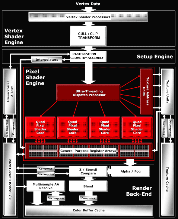


Architecture of vertex processors

There are eight identical vertex processors (they are inside the Vertex Shader Processors unit on the diagram). They comply with SM3 requirements and are based on ATI's standard 3+1 scheme (ALU of each vertex processor can execute two different operations simultaneously over three vector components and the fourth component or a scalar). In fact, vertex processors have become similar to what we saw in NV4X and G7X, but without texture fetching. There is another exception — NVIDIA offers the 4+1 scheme (a four-component vector and scalar are processed per clock), while this solution is based on the 3+1 scheme. The G70 scheme can potentially offer higher performance. But the real difference may be practically unnoticeable, especially now that vertex processors rarely act as a rendering bottleneck.

Architecture of the pixel part

That's the most interesting part. Have a look at the diagram — unlike NVIDIA, the texture units are outside the common pipeline. This architecture may be called distributed. There is no common long pipeline to run quads through, as in case of NVIDIA. The texture part exists separately — texture address units and TMUs. The same concerns pixel processors responsible for math and other operations, and data registers. This scheme has its pros and cons. The main disadvantage — it suits well the phase mechanism, when active texture sampling precedes texture calculations (Shaders 1.X and old programs with stages). But it is fraught with unjustified latencies in dependent texture sampling, which can be often found in modern Shaders 2.X and 3.0. Think about it — one texture fetch command actually calls a lengthy operation for many cycles and the shader processor should stand idle all this time? Nothing of the sort — ATI settles the point smartly! Moreover, it's a universal solution. Not only does it effectively execute dependent samples, it also increases efficiency of the pixel part in shaders with conditions and branches (compared to NVIDIA's approach). ATI calls this technology Hyper-Threading. Let's see how it works...

The magic box (Ultra Threading Dispatch Processor) directs the execution process — it processes 512 quads simultaneously, each of them can be at a different shader execution stage. Each quad is stored together with its current status, current shader command, values of previously checked conditions (information on the current branch of a conditional jump). NVIDIA chips run quads in circle, one after another. The best they can do is to skip quads that don't fall under the current branch of a condition. The R520 operates differently — our magic box constantly monitors free resources (be it texture or pixel units) and directs queued quads into free devices. If a quad fails a condition and should not be processed by this or that shader part, it will not hang about in circles, taking up room and time, together with the other quads, which need to be processed. It will just skip unnecessary commands and will not load a texture or pixel unit. If a quad waits for data from a texture unit — it will let other quads forward, which will load pixel units.

This approach kills two birds with one stone — it hides texture access latency and allows efficient usage of computing and texturing resources when shaders with conditions and branches are executed. Efficiency of both issues depends directly on the number of quads that our magic box can process. 512 looks like an imposing set, we can get textures for four quads and process four quads in pixel processors per cycle; thus up to 8 quads are processed each cycle, while the rest of the quads wait for their turn or wait for data from texture units.

Out of doubt, this unit is complex and the dispatching logic for this quad set takes up a considerable part of the chip, probably comparable with texture and pixel processors. Especially as register arrays actually belong to this unit as well — there must be lots of them to store efficiently all preliminary calculations for the 512 quads in queue.

And now let's examine changes in pixel processors and ALUs. As we have already seen, pixel processors are grouped in four — that is we actually have four quad processors processing four pixels per cycle rather than 16 separate processors. Each quad processor consists of the following units:


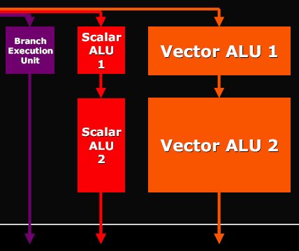
and can execute the following operations over four pixels per cycle:

  • VEC3 ADD + modify and rearrange components (Vector ALU 1)
  • Scalar ADD + modify components (Scalar ALU 1)
  • VEC3 ADD/MUL/MAD and other operations (Vector ALU 2)
  • Scalar ADD/MUL/MAD and other operations (Scalar ALU 2)
  • Conditional or unconditional branch

Besides, don't forget that texture addressing (requesting data from TMU) can be done simultaneously with these five operations. Thus, in case of optimal shader code we get peak performance of six operations per cycle - it's similar to G70, if we take into account the difference in architectural approaches to branch execution. But as we have already mentioned above, the scheme from ATI is better at branching.

Interestingly, ATI is true to its approach — 3+1 (two different operations can be executed, one - over three components of a vector, the other - over a scalar, being the fourth component). In the majority of cases, the approach taken by NVIDIA (an option of 2+2 or 3+1) can be considered more efficient, but this difference will have a little effect on typical graphics tasks.

Another major issue of the new architecture — caching compressed data — Z / Frame buffer data as well as texture data are stored in caches in compressed form. They are decompressed on the fly, when they are accessed from the corresponding units. Thus caching efficiency grows higher. You can say that the cache sizes are virtually increased several-fold.

It would be logical to assume that such an architecture with separated texture and pixel units will be easily scalable:


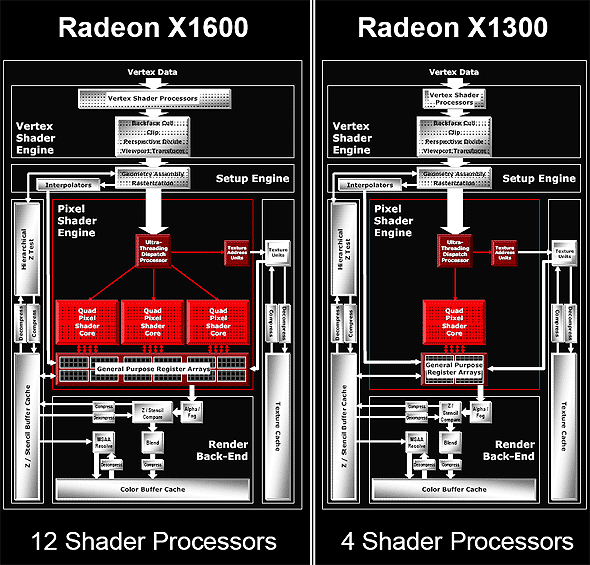
As we can see, RV530 and RV515 are built on the same scheme. There is only one quad left in the RV515 — it simplifies many aspects, including the magic box of the dispatcher. The situation with the RV530 is more complex — it has three pixel quad processors, but only one texture unit. That is we have 12 pixel processors and 4 TMUs, even if used in the optimal way, nearly without downtime. Of course, in case of simple shaders without complex calculations, pixel processors will be idle waiting for texture data. But modern shaders, for which this GPU is intended, are often up to much computing (5-8 commands) per one texture access, justifying this scheme. To all appearances, the number of transistors spent on the texture part of the chip is greater than in case of pixel ALUs. That's why this disbalance is justified from the point of view of ATI engineers.

In fact, giving up 6-8 texture units allows to have 12 (instead of 8 or 4) pixel processors, sticking to the same GPU complexity. How justified it is in practice depends on efficiency of ATI texture units, on efficiency of the dispatcher, and on the ratio of various commands in executed shaders.

Output interfaces

All new graphics cards support HDCP format for both DVI interfaces. Top R520-based models are capable of outputting HDMI (High Definition Media Interface, the interface for outputting video and audio to digital theatres and other audio-video playback devices of the new generation) to DVI connectors. You can read about popular interfaces in our R520 preview.

Conclusions on the R520/RV530/RV515 Architecture

  • New interesting architecture offering high scalability and efficiency of pixel and texture resources
  • There has finally appeared support for SM 3.0. Moreover, sterling operations with an FP16 frame buffer in any modes, including MSAA and texture compression
  • Branches and execution of complex Shaders 3.0 are more efficient than in the latest NVIDIA GPUs. Performance with Shaders 2.0 and lower will be at least comparable, with the odds in favor of ATI on a pipeline basis.
  • Unfortunately, the launch of this series was delayed, which affected competition and popularity of R[V]5XX-based cards. Some cards appeared a couple of months after the announcement
  • Four texture units in the 12-pipeline RV530 seems a disputable decision. Practical tests show that such configuration was not justified for the time the cards were launched on the market.
  • Unfortunately, there is no vertex texture fetch (this feature is available to NV4X and G70), and there is no filtering for FP16 textures

Details: R580, RADEON X1900

R580 Specifications

  • Code name: R580
  • Fabrication Process: 90 nm
  • 384 million transistors
  • FP¡ package (flip-chip, flipped chip without a metal cap)
  • 256 bit memory interface
  • Up to 1 GB of GDDR3 memory
  • PCI-Express x16 bus interface
  • 48 pixel processors
  • 16 texture units
  • Fetching four neighboring texture samples instead of one per cycle, in case of no filtering (it accelerates filtering programmed in a pixel shader, for example, for FP16)
  • Calculating, blending, and writing up to 16 full (color, depth, stencil buffer) pixels per clock
  • 8 vertex processors
  • FP32 processing throughout the pipeline (vertices and pixels)
  • SM 3.0 support, including dynamic branches in pixel and vertex processors. Still no vertex texture fetch.
  • Efficient implementation of jumps and dynamic branches in pixel and vertex processors
  • Support for FP16 format: full support for data output into a frame buffer in FP16 format (including any blending and even MSAA operations). FP16 texture compression, including 3Dc+. Hardware filtering for FP16 texture fetch is not supported!
  • The new integer data type, RGBA (10:10:10:2), for a frame buffer, for higher-quality rendering without FP16
  • New high-quality algorithm of anisotropic filtering (a user is given a choice between a faster or higher-quality anisotropy options), improved trilinear filtering
  • Support for a two-sided stencil buffer
  • MRT (Multiple Render Targets — rendering into several buffers)
  • Memory controller with a 512-bit ring bus, two 256-bit rings in opposite directions (4 memory channels, programmable arbitration)
  • Efficient caching and a new more effective HyperZ implementation (according to ATI, inter-GPU HyperZ buffers were doubled compared to the R520)
  • 2 × RAMDAC 400 MHz
  • 2 × DVI interfaces supporting HDCP as well as HDMI via an adapter
  • TV-Out and TV-In, HDTV-Out
  • Video processor (for video compression, decompression, and post processing), a new generation that can accelerate operations with H.264 — a new algorithm for video compression used in HD-DVD and Blu-Ray video discs
  • 2D accelerator supporting all GDI+ functions
  • ATI CrossFire support

The R580 is sort of a refined modification of the R520. It's the fastest modification with an increased number of pixel processors (a number of texture units remains the same). The only significant difference from the previous ATI flagship is three times as many pixel processors. But the number of texture units was not increased. That is this situation resembles what we had with RV530, where the 3:1 ratio was already obtained, even if with fewer pipelines. Our article analyzes how well this architectural solution performs versus its competitor. It also publishes performance analysis, caused by those additional 32 pixel processors in the R580. You should read about the R520 architecture above, because it's similar to R580, and it's described in more detail.


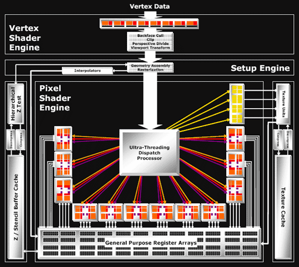
We can see on the diagram more pixel processors. But the number of texture processors remains the same - 4 quads (that is 16 textures fetched per cycle). There is direct evidence of disbalance, which was examined in our reviews by the RV530 example. ATI engineers are of the opinion that it's a reasonable compromise - computing/texturing ratio in modern games may reach 7-to-1 already. It's not easy to say how well this architecture is justified. We check it up in our articles with tests, both synthetic and gaming. We published a unique comparison of R520 and R580 operating at identical frequencies - they differ only in the number of pixel processors. This comparison shows where the additional computing power gives us an advantage, and where it's wasted. It goes without saying that only programmers of future applications will decide whether to prefer computing or no. But it will evidently happen sooner or later.

Details: R580+, RADEON X1950

R580+ Specifications

  • Code name: R580+
  • Fabrication Process: 90 nm
  • 384 million transistors
  • Flip-chip package (flipped chip without a metal cap)
  • 256-bit memory interface
  • Up to 1 GB of DDR2, GDDR3, or GDDR4 memory
  • PCI-Express x16 bus interface
  • 48 pixel processors
  • 16 texture units
  • 8 vertex processors
  • Calculating, blending, and writing up to 16 full (color, depth, stencil buffer) pixels per clock
  • FP32 processing of vertices and pixels
  • SM 3.0 support, including dynamic branches in pixel and vertex processors. The only limitation is no vertex texture fetch
  • Efficient implementation of jumps and dynamic branches in pixel processors
  • Rendering into an FP16 frame buffer, including blending and multisampling; a new integer data type - RGBA (10:10:10:2) for a frame buffer, which provides higher rendering quality without FP16
  • FP16 textures, including texture compression for FP16 textures and the 3Dc+ technology. Hardware filtering for FP16 texture fetch is not supported
  • Fetching four neighboring texture samples instead of one per cycle in case of no filtering (it accelerates filtering programmed in a pixel shader, for example, for FP16 format)
  • New high-quality algorithm of anisotropic filtering (a user is given a choice between a faster or higher-quality anisotropy options), improved trilinear filtering
  • Support for a two-sided stencil buffer
  • MRT (Multiple Render Targets — rendering into several buffers)
  • Memory controller with a 512-bit ring bus, two 256-bit rings in opposite directions, 4 memory channels, programmable arbitration
  • Efficient caching and a more effective HyperZ implementation (according to ATI, HyperZ buffers were enlarged again compared to the R580)
  • 2 × RAMDAC 400 MHz
  • 2 × DVI Dual Link interfaces with HDCP/HDMI support
  • TV-Out and TV-In, HDTV-Out
  • The latest generation of the video processor responsible for compression, decompression, and post processing of video data, supporting hardware-assisted H.264 decoding (the most progressive video format)
  • 2D accelerator supporting all GDI+ functions
  • ATI CrossFire support

Specifications of the reference RADEON X1950 XTX

  • Core clock: 650 MHz
  • Effective memory clock: 2.0 GHz (2*1000 MHz)
  • Memory type: GDDR4, 0.91 ns (the stock frequency is up to 2*1100 MHz)
  • Memory size: 512 MB
  • Memory bandwidth: 64.0 GB/sec
  • Maximum theoretical fillrate: 10.4 gigapixel per second
  • Theoretical texture sampling rate: 10.4 gigatexel per second
  • 2 × DVI-I (Dual Link, 2560×1600 video output)
  • PCI-Express 16x bus
  • TV-Out, HDTV-Out, HDCP support
  • Power consumption: over 100 W, just like the RADEON X1900 XTX

Specifications of the reference RADEON X1950 CrossFire Edition

  • Core clock: 650 MHz
  • Effective memory clock: 2.0 GHz (2*1000 MHz)
  • Memory type: GDDR4, 0.91 ns (the stock frequency is up to 2*1100 MHz)
  • Memory: 512 MB
  • Memory bandwidth: 64.0 GB/sec
  • Maximum theoretical fillrate: 10.4 gigapixel per second
  • Theoretical texture sampling rate: 10.4 gigatexel per second
  • 1 × DVI-I (Dual Link, 2560×1600 video output)
  • PCI-Express 16x bus
  • CrossFire connector
  • Power consumption: over 100 W, just like the RADEON X1900 XTX

It's a modification of the R580. There are few changes this time, none of them significant. The main and only significant difference consists in a modified memory controller and some GDDR4 bug fixes. Now the updated memory controller in the R580+ supports three memory types: DDR2, GDDR3, and GDDR4. According to ATI, the R580+ also has some minor changes: some caches were enlarged, HyperZ now works in up to 2560×1600. The other features remain the same: the number of transistors, pixel/texture/vertex processors, fabrication process. Some time ago many sources assumed that R580+ would be manufactured by the 80 nm fabrication process to cheapen its production costs, reduce its power consumption, and probably to increase its frequency in new products. But these expectations did not come true. Perhaps, the 80 nm fabrication process will be used in the next-gen GPUs (R600) and chips from the other price segments between R580+ and the next generation.

As R580+ is almost an exact copy of the R580, which in its turn was a modified R520 solution, we recommend you read the corresponding reviews: RADEON X1800 (R520) and RADEON X1900 (R580). A CrossFire modification of the card has more differences now. GPU and memory clocks are identical in these cards. The only difference consists in one DVI and CrossFire connector instead of two DVIs and one TV-out. Recommended prices for these two models are also the same, both will come at $449.

As we can see, specifications of R580+ and RADEON X1950 XTX are almost a complete copy of R580 and the RADEON X1900 XTX. The only difference from ATI's previous top model is GDDR4 memory. The core clock remains the same. The RADEON X1950 XTX and the RADEON X1900 XTX operate at the same clock - 650 MHz. But memory clock has been changed to 1000(2000) MHz, which seemed unattainable not long ago. Such a high operating frequency has become possible owing to the new memory type. The reference card RADEON X1950 XTX uses GDDR4 memory chips with 0.9 ns access time, which corresponds to 1100(2200) MHz. It's a tad higher than the operating frequency in our model.

GDDR4 (Graphics Double Data Rate, Version 4) - a new generation of graphics memory, designed for 3D graphics cards. It's almost twice as fast as GDDR3. The main differences between GDDR4 and GDDR3 are increased operating frequencies (consequently, higher bandwidth) and reduced power consumption. Technically, GDDR4 memory does not differ much from GDDR3. It's just another evolutional step, which simplifies adaptation of the existing chips and development of future products supporting this new memory type. The RADEON X1950 XTX has become the first graphics card with GDDR4 chips. NVIDIA is planning to launch such products a tad later. They will most likely be graphics cards based on NVIDIA G80.

The new memory type has been developed by Samsung and Hynix in cooperation with ATI, which orchestrated the process within the bounds of JEDEC. GDDR4 chips are currently manufactured by these two companies. But only Samsung has started their production on a mass scale. Big memory shipments to graphics card manufacturers started not long ago. Production of 1.2(2.4) GHz modules has been commenced in June. The company also announced its successful development of (1.6)3.2 GHz chips, twice as fast as GDDR3 can offer. Samsung currently manufactures three types of GDDR4 memory: 0.71 ns, 0.83 ns, and 0.91 ns ones, with operating frequencies varying from 1100(2200) to 1400(2800) MHz. We can only hope that problems with availability of GDDR4 memory (it's manufactured in limited volumes) will be solved.

Advantages of the new memory modules over GDDR3 include not only performance - their power consumption is approximately 30-40% as low as the one demonstrated by GDDR3. Lower power consumption of GDDR4 memory allows to relieve requirements to power supply and cooling, or to increase power consumption of a GPU and retain the overall power consumption of the card. Power consumption can be reduced owing to lower nominal voltage VDD for GDDR4 - 1.5 V. So we can speak of power saving compared to GDDR3. But early chips installed on the RADEON X1950 cards use 1.8 V, just like GDDR3 memory. The most powerful solutions may use 1.9 V. That's why the X1950 XTX now consumes no less than the X1900 XTX, even though GDDR4 potentially consumes less power than the previous version of graphics memory.

Increased memory frequency resulted in higher bandwidth. It's 64 GB/s for the RADEON X1950 XTX, higher than in any other single-GPU graphics card. For comparison, memory bandwidth of the NVIDIA GeForce 7800 GTX is 51.2 GB/s, the GeForce 7800 GTX 512Mb - 54.4 GB/s (the latter is equipped with the fastest GDDR3 memory). GDDR4 memory installed on the RADEON X1950 XTX has almost a 30% advantage in memory bandwidth over the previous flagship from ATI. It allows the new solution to enjoy a 15% advantage over the X1900 XTX under a heavy video memory load, such as high resolutions with antialiasing.

Details: RV570, RADEON X1950 PRO

RV570 Specifications

  • Code name: RV570
  • Fabrication Process: 80 nm
  • 330 million transistors
  • 256-bit memory interface
  • Supports DDR, DDR2, or GDDR3 memory
  • PCI-Express x16 bus interface
  • 36 pixel processors
  • 12 texture units
  • 8 vertex processors
  • Calculating, blending, and writing up to 12 full (color, depth, stencil buffer) pixels per clock
  • FP32 processing of vertices and pixels
  • SM 3.0 support, including dynamic branches in pixel and vertex processors. The only limitation is no vertex texture fetch
  • Efficient implementation of jumps and dynamic branches in pixel processors
  • Rendering into an FP16 frame buffer, including blending and multisampling; a new integer data type - RGBA (10:10:10:2) for a frame buffer, which provides higher rendering quality without FP16
  • FP16 textures, including texture compression for FP16 textures and the 3Dc+ technology. Hardware filtering for FP16 texture fetch is not supported
  • Fetching four neighboring texture samples instead of one per cycle in case of no filtering (it accelerates filtering programmed in a pixel shader, for example, for FP16 format)
  • High-quality algorithm of anisotropic filtering (a user is given a choice between a faster or higher-quality anisotropy options), improved trilinear filtering
  • Support for a two-sided stencil buffer
  • MRT (Multiple Render Targets — rendering into several buffers)
  • Efficient caching and a more effective HyperZ implementation
  • 2 × RAMDAC 400 MHz
  • 2 × DVI Dual Link interfaces with HDCP/HDMI support
  • TV-Out and TV-In, HDTV-Out
  • The latest generation of the video processor responsible for compression, decompression, and post processing of video data, supporting hardware-assisted H.264 decoding (the most progressive video format)
  • 2D accelerator supporting all GDI+ functions
  • Integrated support for ATI CrossFire

Specifications of the reference RADEON X1950 PRO

  • Core clock: 580 MHz
  • Effective memory frequency: 1.4 GHz (2*700 MHz)
  • Memory type: GDDR3, 1.4 ns (the stock frequency is 2*700 MHz)
  • Memory: 256 MB
  • Memory bandwidth: 44.8 GB/sec
  • Maximum theoretical fillrate: 7.0 gigapixel per second
  • Theoretical texture sampling rate: 7.0 gigatexel per second
  • 2 × DVI-I (Dual Link, 2560×1600 video output)
  • PCI-Express 16x bus
  • TV-Out, HDTV-Out, HDCP support

Details: RV560, RADEON X1650 XT

  • Code name: RV560
  • Fabrication Process: 80 nm
  • 330 million transistors
  • 128-bit memory interface
  • Supports DDR, DDR2, or GDDR3 memory
  • PCI-Express x16 bus interface
  • 24 pixel processors
  • 8 texture units
  • 8 vertex processors
  • Calculating, blending, and writing up to 8 full (color, depth, stencil buffer) pixels per clock
  • FP32 processing of vertices and pixels
  • SM 3.0 support, including dynamic branches in pixel and vertex processors. The only limitation is no vertex texture fetch
  • Efficient implementation of jumps and dynamic branches in pixel processors
  • Rendering into an FP16 frame buffer, including blending and multisampling; a new integer data type - RGBA (10:10:10:2) for a frame buffer, which provides higher rendering quality without FP16
  • FP16 textures, including texture compression for FP16 textures and the 3Dc+ technology. Hardware filtering for FP16 texture fetch is not supported
  • Fetching four neighboring texture samples instead of one per cycle in case of no filtering (it accelerates filtering programmed in a pixel shader, for example, for FP16 format)
  • High-quality algorithm of anisotropic filtering (a user is given a choice between a faster or higher-quality anisotropy options), improved trilinear filtering
  • Support for a two-sided stencil buffer
  • MRT (Multiple Render Targets — rendering into several buffers)
  • Efficient caching and a more effective HyperZ implementation
  • 2 × RAMDAC 400 MHz
  • 2 × DVI Dual Link interfaces with HDCP/HDMI support
  • TV-Out and TV-In, HDTV-Out
  • The latest generation of the video processor responsible for compression, decompression, and post processing of video data, supporting hardware-assisted H.264 decoding (the most progressive video format)
  • 2D accelerator supporting all GDI+ functions
  • Integrated support for ATI CrossFire

Specifications of the RADEON X1650 XT

  • Core clock: 600 MHz
  • Effective memory frequency: 1.4 GHz (2*700 MHz)
  • Memory type: GDDR3, 1.4 ns (the stock frequency is 2*700 MHz)
  • Memory: 256 MB
  • Memory bandwidth: 22.4 GB/sec
  • Maximum theoretical fillrate: 4.8 gigapixel per second
  • Theoretical texture sampling rate: 4.8 gigatexel per second
  • 2 × DVI-I (Dual Link, 2560×1600 video output)
  • PCI-Express 16x bus
  • TV-Out, HDTV-Out, HDCP support

Both GPUs belong to the new generation, they are manufactured by the 0.08 µm fabrication process. The core is absolutely the same in size and the number of transistors. Physically, RV560 and RV570 are the same GPUs in different packages. The RV560 uses a 128-bit package for X1600 PCBs (these chips are cut down - one third of pixel and texture units). And the RV570 is packaged for 256 bit with a protective frame, for simplified X1900 PCBs.

The new Mid-End GPUs from ATI were delayed several times. Perhaps it had to do with the new fabrication process - in other respects they have nothing new. The RV570 is almost identical to the existing RADEON X1900 GT, which is based on the cut-down R580. Now it's replaced with the RV570 with its 36 pixel and 12 texture units, that is featuring the same ratio of pixel/texture shaders used in the latest ATI solutions. But the chip has become much smaller, and its manufacturing is now much cheaper. The core clock remains the same, while the memory frequency has grown from 1200 MHz to 1400 MHz. The X1950 PRO has a similar PCB design to the one used in expensive X1900 cards. But the PCB was significantly simplified. Memory chips were rotated by 90°. The power supply unit is also simplified - it now has fewer analog elements. As the new GPUs are cheaper, and their PCB design is simplified, we get a good solution with the recommended price of $199.

The RADEON X1650 XT takes up the place of the X1600 XT, which was renamed into the X1650 PRO. That is, the X1650 PRO and the X1650 XT are not based on the same chip operating at different frequencies, as we had thought, but they are two absolutely different GPUs. The X1650 PRO is based on RV530 with 12 pixel, 5 vertex, and 4 texture units. And the new card is based on RV560 with 24 pixel, 8 vertex, and 8 texture units. Some characteristics have grown almost twofold, but memory frequency and memory bus width are the same. So the computing power has grown much, while memory bandwidth may hamper performance significantly. If we take into account the recommended price of $149, this solution will be interesting anyway. The X1650 XT PCB differs from the board used in the X1600 and X1650 cards only in the layout of CrossFire connectors, because RV560 does not require a master card to support this mode. The other elements of design are not modified, except for a number of power line nuances.

It should be mentioned that designs of both PCBs (for RV560 and RV570) now have connectors for special CrossFire cables. Support for CrossFire without master cards and GPUs is integrated into the GPU. There has finally appeared an option to join two usual ATI cards into CrossFire, as NVIDIA SLI has allowed from the very beginning. PCB designs allow to plug two adapters or a single wide adapter. The matter is that SLI can transmit signals only one way at a time, while the new CrossFire is able to send them both ways simultaneously. Besides, adapters will be actually flexible cables. So the distance between graphics cards doesn't matter. And SLI usually uses rigid adapters of fixed length.


Reference Information on RADEON R[V]4XX Graphics Cards
Reference Information on RADEON R[V]5XX Graphics Cards
Reference Information on RADEON R[V]6XX Graphics Cards


Alexander Medvedev (unclesam@ixbt.com)

Alexei Berillo (sbe@ixbt.com)

Updated on August 6, 2007


Write a comment below. No registration needed!


Article navigation:


blog comments powered by Disqus

  Most Popular Reviews More    RSS  

AMD Phenom II X4 955, Phenom II X4 960T, Phenom II X6 1075T, and Intel Pentium G2120, Core i3-3220, Core i5-3330 Processors

Comparing old, cheap solutions from AMD with new, budget offerings from Intel.
February 1, 2013 · Processor Roundups

Inno3D GeForce GTX 670 iChill, Inno3D GeForce GTX 660 Ti Graphics Cards

A couple of mid-range adapters with original cooling systems.
January 30, 2013 · Video cards: NVIDIA GPUs

Creative Sound Blaster X-Fi Surround 5.1

An external X-Fi solution in tests.
September 9, 2008 · Sound Cards

AMD FX-8350 Processor

The first worthwhile Piledriver CPU.
September 11, 2012 · Processors: AMD

Consumed Power, Energy Consumption: Ivy Bridge vs. Sandy Bridge

Trying out the new method.
September 18, 2012 · Processors: Intel
  Latest Reviews More    RSS  

i3DSpeed, September 2013

Retested all graphics cards with the new drivers.
Oct 18, 2013 · 3Digests

i3DSpeed, August 2013

Added new benchmarks: BioShock Infinite and Metro: Last Light.
Sep 06, 2013 · 3Digests

i3DSpeed, July 2013

Added the test results of NVIDIA GeForce GTX 760 and AMD Radeon HD 7730.
Aug 05, 2013 · 3Digests

Gainward GeForce GTX 650 Ti BOOST 2GB Golden Sample Graphics Card

An excellent hybrid of GeForce GTX 650 Ti and GeForce GTX 660.
Jun 24, 2013 · Video cards: NVIDIA GPUs

i3DSpeed, May 2013

Added the test results of NVIDIA GeForce GTX 770/780.
Jun 03, 2013 · 3Digests
  Latest News More    RSS  

Platform  ·  Video  ·  Multimedia  ·  Mobile  ·  Other  ||  About us & Privacy policy  ·  Twitter  ·  Facebook


Copyright © Byrds Research & Publishing, Ltd., 1997–2011. All rights reserved.