 |
||
|
||
| ||
|
||
|
||
| ||
Reference Information on RADEON R[V]4XX Graphics Cards R[V]6XX Specifications
Specifications of reference cards based on R[V]6XX
* - The unified architecture implies having unified processors stream-process vertices, pixels, and other data. Details: R600, RADEON HD 2900 SeriesR600 Specifications
Reference RADEON HD 2900 XT Specifications
Details: RV630, RADEON HD 2600 seriesRV630 Specifications
RADEON HD 2600 XT Specifications
RADEON HD 2600 PRO Specifications
Details: RV610, RADEON HD 2400 SeriesRV610 Specifications
RADEON HD 2400 XT Specifications
RADEON HD 2400 PRO Specifications
R600/RV630/RV610 ArchitectureThe R6xx architecture combines some old solutions (R5xx and Xenos - GPU from Microsoft Xbox 360) and various innovations: a more powerful dispatch processor, super scalar architecture of shader processors with dedicated branch execution units, an updated 512-bit ring bus. That's how the architecture of the top R600 GPU looks like: 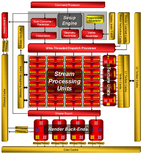 We can see that the main computing power is 64 superscalar streaming processors, each one containing five ALUs and a dedicated branch execution unit. AMD prefers to specify their number in total - 320 stream processing units. We all know that manufacturers like to publish large numbers. So the peak performance of a single R600 is said to be 475 GigaFLOPS. This result is hardly attainable in real algorithms. The Ultra-Threaded Dispatch Processor controls how the execution units process streams. It decides how to load a given unit depending on requirements and priorities. The new dispatch processor, implemented in R6xx, can service thousands of streams simultaneously. Here is its diagram: 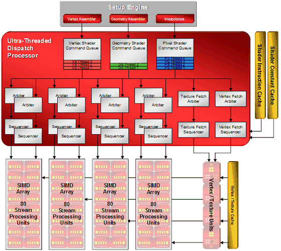 The other changes from previous generations include the Command Processor, which processes commands of a video driver. It executes microcode to offload a CPU and to increase performance in case of many draw calls with few processed geometry (the small batch problem in Direct3D). The effect from the command processor is said to appear in Direct3D 9 and Direct3D 10 applications. Theoretically, reducing overheads on various checks may bring up to 30% of performance gain. But the real numbers will certainly be much lower. The new architecture seems to scale well both ways, we can see it in low-end and mid-end solutions. Diagrams of RV630 and RV610: 

I wonder how real applications will balance the load between vertex, pixel, and geometry shaders - in case of the unified architecture, developers must take care of the efficient distribution of streaming processors between various types of shaders. When performance is limited by pixel computations, an increased load on vertex units of the traditional architecture does not result in a performance drop. What concerns the unified architecture, it will change the balance so that fewer resources will be available to pixel computations. Shader Processors (ALU)In the previous generation of its GPUs, ATI changed the traditional design used by NVIDIA. R580 contained 48 shader units and 16 texture units, while G70 used to have 24 TMUs and pixel processors and 16 ROPs. In fact, this difference in the approaches appeared in the times of RV530/RV560, which also had this ratio of TMUs and shader processors. NVIDIA traditionally pays a tad more attention to texturing and fill rate, while AMD(ATI) prefers pixel and vertex operations. Shader processors in the previous ATI solutions contained vector and scalar execution units that could execute two instructions per cycle over 3+1 or 4+1 components. And now each processor (out of 64) can execute five instructions over five components. Each stream processing unit consists of five independent scalar ALUs, which can execute five MAD (Multiply-Add) instructions per cycle. One of five ALUs can execute a more complex instruction: SIN, COS, LOG, EXP, etc. The processor also contains a branch execution unit that offloads ALUs and clears performance drops from jumps in the shader code. 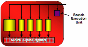 R6xx GPUs have standard ALUs for DirectX 10 solutions, FP32 precision, support for computations in new integer formats, IEEE 754 compliance (important for scientific, statistical, economical, and other computations.) The number of these execution units in R600 is very big. But compared to the rival solution from NVIDIA, we should take into account its doubled frequency of shader processors. We should also be careful with the comparison of scalar and superscalar architectures. Both of them have pros and cons. For example, each unit in the superscalar architecture can process several independent instructions (up to five math instructions and one branch in our case) per cycle. But this architecture has a weakness - an application and a driver must feed it constantly with as many independent instructions as possible to keep the units working and maintain high efficiency. The scalar architecture does not have this limitation. It's more flexible. Its efficiency will always be higher, because 3D applications use various combinations of commands, many of which depend on preceding commands. So it's not easy to feed 4-5 independent commands in succession. In order to raise efficiency of a superscalar architecture, we need a high-quality optimizing recompiler for shaders and optimizations in applications. A bright example here is the NV3x superscalar architecture, which benefits much from its recompiler and optimizations. R6xx does not have such crying bottlenecks as in NV3x, of course. But its architecture still benefits from optimizations. In fact, it's wrong to compare so different modern architectures only by the number of execution units. We should analyze results of synthetic tests and games. And it must be perfectly clear what they mean and what units in what test act as bottlenecks. All these big figures are important for marketing rather than for determining the real speed. TMUThe R6xx architecture uses new texture units (to be more exact, texture/vertex fetch units in the unified chips). They are separated from the stream processors, so they can start fetching data before they are requested by a shader unit (the dispatch processor is in charge of everything, so it can set a task ahead of time), which can theoretically raise performance. R6xx texture units have the following configuration (by the example of the top R600 GPU): 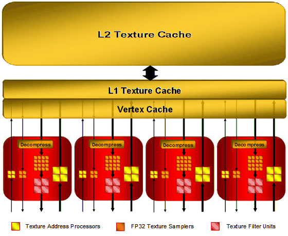 There are four texture units all in all, each unit consists of the following elements: 8 texture address units (32 in total), 20 texture samplers (80 in total), 4 filter units (16 in total). Vertices and textures are usually sampled separately. Some texture address units and texture samplers in a TMU are intended for vertices (they are not connected with filter units on the diagram) or for non-filtered textures. Four texture address processors and four texture samplers in each TMU work with vertex fetches, which do not need texture filter units. The remaining four texture address processors, 16 texture samplers, and four filter units belong to texture fetches, which need filtering. That is 64 out of 80 texture samplers fetch 16 pixels for 16 filter units. And the remaining 16 units fetch vertex data (or textures without filtering). As TMUs are separated from ALUs in the R6xx GPUs, they can fetch vertices and pixels at the same cycle. Each sampler can fetch one value per cycle, and a texture filter unit can filter one 64-bit value per cycle or one 128-bit value each two cycles. Considering the above-mentioned details, each unit can sample up to two texels per cycle, if one of them does not require filtering. As you can see on the diagram, texture fetches use two-level caches. L2 texture caches, shown on the diagram, have the following capacities: 256 KB in R600, 128 KB in RV630. RV610 use one cache level, shared by vertex and texture data. Vertex cache in R600 is said to be enlarged eightfold versus the one used in R580. It's done because performance of unified processors allows to process data several times faster than dedicated units of geometry shaders in previous architectures. Texture units in the R6xx GPUs are improved. One of their main advantages is that they can sample and bilinear-filter FP16 textures at the same speed as 32-bit ones, FP32 textures - at half the speed, that is like in G80. These GPUs support new 32-bit HDR texture formats, which appeared in DirectX 10; trilinear and anisotropic filtering for all supported texture formats. Maximal resolution of textures has reached 8192x8192 (as in G80). Company representatives speak of higher quality of texture filtering. We'll test it in one of the next parts of this article. By the way, AMD materials do not mention free trilinear filtering, so it most likely reduces peak performance of TMUs, like in all GPUs except G80. Texture units in RV630 and RV610 offer the same functionality as units of the top solution from this family (except for cache implementation in RV610), but there are fewer of them. The number of TMUs is one of potential weak spots of the new family. High computing performance is good, of course. But this power alone is necessary only for non-graphical calculations. Texture sampling rate and filtering speed are still very important for 3D graphics. Modern games use not only complex pixel and vertex shaders, they also apply several textures per pixel: main textures, specular textures, normal maps, bump maps, cubic maps of reflections and refractions, etc. Sixteen texture units may be insufficient for such a powerful GPU as R600 to reveal its computing potential. We'll check it up in synthetic and game tests. ROPROP units in the R6xx did not suffer many changes compared to the previous GPUs. The R600 has four ROPs. Each unit writes four pixels. So we've got 16 processed pixels written into a frame buffer. RV630 and RV610 have one ROP, it can write only four pixels. ROPs support double performance in Z-only mode, that is 32 pixels for R600 and 8 pixels for RV610/RV630 correspondingly. It can use up to eight MRTs (rendering buffers) with multisampling. This requirement is put forward by DirectX 10, so we cannot expect other numbers here. There is sterling support for rendering into a FP16/FP32 frame buffer, of course, including antialiasing. 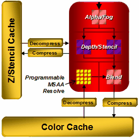 What concerns interesting innovations in ROPs, AMD declares improved compression of Z and stencil buffers, up to 16:1 versus 8:1 in previous solutions, and up to 128:1 with MSAA 8x. Data in Z and stencil buffers are compressed separately to increase compression efficiency. The resolution threshold available for compression was also traditionally increased. It had been limited to 5 Mp, but now this threshold is not specified. A lot of optimizations were added for Z buffer. Most of them accelerate stencil shadows in popular applications (DOOM 3, F.E.A.R., Unreal Engine 3, etc). We'll benchmark R600 in them in our article. New antialiasing modesThe R6xx chips support multisampling with eight samples maximum. In order to keep up with its rivals and CSAA, engineers introduced new modes with up to 24 samples, Custom Filter Anti-Aliasing (CFAA). These are special post processing modes intended to improve antialiasing quality, with programmable layout of subpixels, sampling outside pixel borders, various sample weights.  Depending on a selected mode, CFAA chooses 4-8 neighboring samples outside a pixel. Even though these samples have lower weights than internal samples, this method will still blur the entire image. The more samples outside a pixel, the blurrier an image. One of the key advantages of this approach is improving antialiasing quality with driver updates. Besides, multisampling control options will become available to developers in the next versions of DirectX. It goes without saying that all previously added features (adaptive antialiasing, temporal antialiasing, gamma correction for MSAA, etc) are also supported by the new GPUs. The main drawback of CFAA is that additional samples outside pixel borders may deteriorate image quality. Remember the special antialiasing mode called Quincunx in NVIDIA cards? It also used sampling outside pixel borders and blurred the image, so most people didn't like it. AMD's approach is more flexible, of course. Samples outside pixel borders will have lower weights than those inside a pixel. But the image will still be blurred. We'll see whether the effect will be irritating in a section devoted to render quality. In our opinion, there is a more interesting new antialiasing feature in the R6xx GPUs. It's not ready in current drivers yet - antialiasing with the edge detect adaptive filter. In this case, a rendered image is filtered with edge detection. Pixels with high frequencies detected by the filter (polygon borders and sharp transitions on some textures that usually need antialiasing) use higher-quality antialiasing method with more samples, the other pixels use fewer samples. This approach resembles the one used in FAA from Matrox Parhelia. Theoretically, it must demonstrate excellent results, both in antialiasing quality and in performance, because it works intensively exactly where it should, it reduces texture noise, and it shouldn't deteriorate details. But this is theory, we'll see what's going on in practice in the quality section of the article. 512-bit ring busOne of indubitable advantages of the R600 is its 512-bit ring bus. It's the first video chip supporting 512-bit access to video memory. Now the ring bus includes eight 64-bit channels connected with an internal 1024-bit bus (two 512-bit directions), there is no central hub. This solution scales well and provides very high effective bandwidth. It's over 100 GB/s for the first R600-based graphics cards with usual, not-very-fast GDDR3 memory. This figure may grow in future solutions, because the controller supports fast GDDR4 memory. 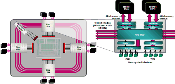 AMD representatives say that the ring bus is modified to reach higher efficiency. These results can be obtained with a 384-bit bus, of course, as NVIDIA did in the GeForce 8800 Ultra. But it requires much more expensive and rare memory. On the other hand, the 512-bit solution has a drawback - it requires a more complex PCB, as well as a more expensive manufacturing process. In return, high bandwidth will certainly show its worth in high resolutions, with high-level antialiasing, and HDR. We can expect a higher advantage of the RADEON HD 2900 XT over NVIDIA rivals in these resolutions. Programmable tessellatorXenos inheritance of the R6xx shows in a programmable tessellator in the RADEON HD 2000 cards. It's a new unit for PCs. You can learn basic information about tessellation in the following articles:
Tessellation is used to increase geometric complexity of models, to make complex models out of low-polygon ones. Tessellation can reduce expenses on animation, add details to models at a small performance costs, improve LOD algorithms. A fully hardware solution allows developers send data to a GPU with fewer details. Then a GPU tessellates them to necessary complexity and applies displacement mapping (see the link above). It reduces the load on a CPU and the amount of data transferred via the buses. Tessellation does not have a single algorithm, it can be done with several methods. There are several types of higher order surfaces: Bezier, N-Patches, B-Spline, NURBs, subdivision surfaces, which can be split into polygons by a GPU. As the tessellator in the R6xx GPUs can be programmed, it can be used for various algorithms, which gives more flexibility and control to 3D developers. AMD publishes the following flow chart of the pipeline:  The R6xx GPUs do not need new shader types in API to use the tessellator, the required vertex shader is written by developers. I don't understand how a usual vertex shader does tessellation. But it's up to developers to understand. The programmable tessellator has big advantages. Tessellation can raise geometry details of a scene without a significant increase of bus and CPU loads. Tessellation is especially effective in combination with displacement mapping. But this is all theory, reality is usually much less peachy. I wonder how to use the tessellator in different APIs (Direct3D 9, Direct3D 10, OpenGL). But the most important question is whether developers will use GPU features of one of two vendors. Games ported from Xbox 360, which use tessellation on the native platform, will certainly benefit from it. But what about the other graphics cards? Improved CrossFire supportWhile we're describing peculiarities of the new solutions from AMD, we should also mention the improved support for CrossFire. All new GPUs do not need special master cards. At last native CrossFire support has appeared in GPUs of this family in all price ranges. As in case with RV570-based cards, users can connect usual graphics cards with bridges (similar to those used for NVIDIA SLI). The new GPUs support all old rendering modes: Alternate Frame Rendering, SuperTile, Scissor, SuperAA. Maximum resolution in CrossFire modes is 2560x2048@60 Hz. The most interesting thing in the description of the updated CrossFire is its support for more than two GPUs rendering the same image. We'll gladly test it, when we have an opportunity. ATI Avivo HDThere are also some improvements in multimedia features of the new GPUs. All R6xx GPUs contain special units: UVD (Universal Video Decoder) and AVP (Advanced Video Processor). ATI Avivo technology has been preserved. Like PureVideo in competing products, it develops and expands. Now it has got a fashionable addon - ATI Avivo HD. The previous generation of GPUs can only accelerate some video decoding stages, leaving the most resource-intensive stages to a CPU. The new generation of GPUs features a dedicated unit for video decoding (UVD), which does all the main work: hardware-assisted statistical decoding VLC/CAVLC/CABAC, iDCT, motion compensation, and deblocking, to offload a CPU and a 3D pipeline of a GPU. The latter is especially important for Windows Vista, which uses 3D features of graphics cards to draw the Aero interface. The entire family of new GPUs support the updated technology. They offer fully hardware-assisted decoding of resource-intensive video formats (H.264 and VC-1) with the highest bitrate - main formats for Blu-ray and HD-DVD. Support for hardware-assisted video decoding is expanded with the above-mentioned new units. Unlike the previous generations of Avivo, they can execute statistical decoding functions (very important for modern video formats) on the hardware level. ATI Avivo HD technology allows to decode all mentioned formats with the resolution of up to 1920x1080 at 30-40 Mbps. Everything necessary is supported by all GPUs of this family. AMD publishes the following table, where is compares its GPUs with competing products:  Unlike similar video processing units in NVIDIA G84 and G86, AMD solutions support hardware-assisted statistical decoding of the VC-1 format. he company publishes similar CPU load figures as NVIDIA. According to their data, fully software decoding of HD DVD loads a modern dual core processor by 80%. Hardware-assisted video decoding in prev-gen GPUs loads a CPU by 60-70%. And a purely hardware solution (UVD) loads a CPU by a little more than 10%, which allows to play all existing discs even on mediocre PCs. We'll try to check it up in our articles. And now we can only take it on trust. Non-graphical computationsHuge floating-point math performance of modern graphics cards and flexibility of unified architectures gave impetus to GPU usage in computing physics in games and serious applications: mathematical and physical modelling, economic and statistic models and calculations, OCR, image processing, science graphics, etc. That's why all GPU manufacturers have paid much attention to non-graphical computations on graphics cards of late. ATI(AMD) launched special RADEON X1900 cards (Stream Processor) based on R580 with 1 GB of GDDR3. The new GPUs possess all necessary features for such products, of course. Even their higher floating-point computing power can be used in many applications: computing physics in games, processing media data (for example, re-encoding, capturing and encoding HD video) and images, voice recognition and OCR, medicine tasks (virtual endoscopy, interactive visualization), meteorology, liquid/gas dynamics, etc. Perhaps, the RADEON HD 2000 cards will be followed by new "Stream Processor" products based on R600 with support for integer and floating-point computing (it appeared in the new architecture), which will use the significantly increased power of 320 stream processors. Abbreviated list of new features in the R6xx GPUs, which are important for non-graphical computing: integer operations, support for 8192x8192 textures, unlimited shader length, unlimited memory for registers, command processor to reduce time losses on checking calls and states. In a little digression we again complain about the lack of real examples of GPUs computing physics in games. We just don't feel like publishing images provided by GPU manufacturers, because nothing has changed for common users - GPUs are unfortunately useless for non-graphical computing in modern games. Support for HDMI and other external interfacesOne of long-awaited solutions in the HD 2000 family is the built-in audio chip necessary for transmitting audio via HDMI. Solutions based on R600, RV610, or RV630 do not need external audio and corresponding cables, there is no need to transmit audio from an integrated solution or an external sound card to the motherboard. Besides, Vista Premium certification requires the entire audio section to be integrated and HDCP-protected. AMD's solution supports the following 16-bit PCM formats: 32 kHz, 44.1 kHz, and 48 kHz, as well as AC3 compressed streams, such as Dolby Digital and DTS. Transmitting video and audio signals via the same HDMI connector can be convenient in many cases - a single cable replaces many wires. Interestingly, the HD 2000 cards do not have HDMI connectors, only DVI. A special bundled DVI-to-HDMI adapter is used to output HDMI signal, it's also used for audio output (it's a digital format, its bandwidth is sufficient both for video and audio). Usual adapters cannot do that. The new adapters are compatible with usual DVI without audio. This new feature is really useful, but not in all cases. It will be necessary in Mid- and Low-End cards, which can be installed into small and quiet barebones used as media centers. Because there is no need to buy a High-End graphics card just to watch video on a big HDTV screen. The RADEON HD 2400 and HD 2600 cards may become popular owing to their built-in audio, because these solutions offer excellent video decoding features and can transmit protected video and audio via the same HDMI connector. Unlike the NVIDIA GeForce 8800, all new AMD solutions support Dual-Link DVI outputs with HDCP. Just like the GeForce 8600 GTS, which was the first graphics card with such features. Top graphics cards come with two DVIs with bundled DVI-to-HDMI adapters. Cheap cards use a conservative solution - one D-Sub and one DVI. Details: RV670, RADEON HD 3800 SeriesRV670 Specifications
RADEON HD 3870 Specifications
RADEON HD 3850 Specifications
RV670 ArchitectureYou can read about architectural peculiarities of AMD R6xx family above. RV670 offers the same features as the previous solutions (320 unified processors, 16 texture fetch units, 16 ROPs, programmable tessellator, etc), but with minor changes to support Direct3D 10.1, they will be described below. The diagram of RV670 is absolutely identical to that of R600. In fact, RV670 does not differ from R600 at all, it has just as many units (ALU, ROP, TMU). The only setback in the new mid-end GPU is no support for a 512-bit bus. It can use only a 256-bit one. The other features described in this article can be applied to the new product without any reservations. Of course, AMD claims that the controller in RV670 has been optimized for more efficient usage of bus bandwidth, that the 256-bit bus operates as a 512-bit one inside, etc. One of the slides at the presentation even runs that the equally-clocked HD 3870 performs on a par with RADEON HD 2900. Direct3D 10.1 SupportThe updated DirectX version will be released only in the first half of 2008, together with the service pack for MS Windows Vista. Service Pack 1 with DirectX 10.1 will take time to appear, to say nothing of new API features in real games. The main changes in this version are some improvements: Shader Model 4.1, independent blending modes for MRT, cube map arrays, reading and writing values to buffers with MSAA, fetching several texture values simultaneously - Gather4 (previously known as FETCH4 in ATI GPUs), mandatory blending for integer 16-bit formats and filtering for 32-bit floating-point formats, support for MSAA with at least four samples, etc. The new features of DirectX 10.1 will facilitate some rendering techniques (for example, global illumination in real time). All new features can be divided into the following groups: improvements in shading and texturing, changes in antialiasing and specifications. Let's go into details now.
As we have already mentioned above, some of the new features in DirectX 10.1 simplify implementation of algorithms to raise 3D graphics quality. For example, AMD gives an example of global illumination (Global Illumination, GI) and ambient occlusion, they are described in detail in the baseline article about RV670. The advantage of DirectX 10.1 in computing GI is as follows: developers can use cube map arrays with geometry shaders in an efficient real-time GI algorithm. DirectX 10.1 also allows to use special antialiasing filters from pixel shaders. Such methods improve image quality when a regular MSAA algorithm runs into problems, for example, in case of HDR or deferred shading. Such algorithms use access to all screen buffers from shaders that appeared in DX 10.1, the previous version allowed to read and write data only to multisampling color buffers. Direct3D 10.1 allows to read and write data from Z buffer for each sample, so 3D developers can use advanced antialiasing methods in their algorithms and even combine regular and shader antialiasing methods. Many innovations in DirectX 10.1 are very useful. But we should not forget that the updated API will appear only in six months, graphics card with its support will also take some time to appear in stores (by the way, NVIDIA plans to launch DirectX 10.1 cards in the next GPU generation, which representatives will appear only after Service Pack 1 for Vista). Besides, the first graphics cards will not support all features of the new API fast enough for real applications. PCI Express 2.0RV670 features PCI Express 2.0 bus support. The second version of PCI Express doubles the standard bandwidth from 2.5 Gbps to 5 Gbps. As a result, the standard x16 slot for graphics cards can transfer up to 8 GB per second in each direction (marketing specialists like to sum up these numbers to 16 GB/s), unlike 4 GB/s provided by PCI Express 1.x. Besides, PCI Express 2.0 is compatible with PCI Express 1.1. Old graphics cards will work with new motherboards, and new graphics cards will still support old motherboards. Provided the external power is sufficient, of course. Besides, you won't enjoy the double bandwidth of the interface. It's not easy to evaluate the real effect of higher PCI Express bandwidth on performance, we need tests in identical conditions, which is a tricky part. But higher bandwidth won't hurt, especially for SLI/CrossFire systems that use PCI Express as one of the ways to exchange data. Many modern games require lots of fast memory, so when the local video memory is not enough, they use system memory. In this case PCI Express 2.0 will be quite helpful. 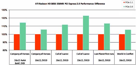 AMD publishes the following data for RADEON HD 3850 with 256 MB of memory: performance difference between systems with PCI Express 1.x and 2.0 in Company of Heroes, Call of Juarez, Lost Planet, and World In Conflict varies from 5% to 25%, about 10% on the average. It happens in high resolutions, of course, when the frame buffer and ancillary buffers take up most of the local video memory, and some resources are stored in system memory. To provide backward compatibility with existing PCI Express 1.0 and 1.1 solutions, Specs 2.0 support both 2.5 Gbps and 5 Gbps modes. Backward compatibility with PCI Express 2.0 allows to use old 2.5 Gbps solutions in 5.0 Gbps slots, which will work at lower speed. Devices compliant with Specs 2.0 support both 2.5 Gbps and 5 Gbps speeds. As it usually happens, it sounds great, but in practice there may be possible compatibility problems with some combinations of motherboards and expansion cards. ATI PowerPlayAnother real improvement for common users is the ATI PowerPlay technology - it's dynamic power management technology that came from GPUs for notebooks. A special control circuit in a GPU monitors its load (by the way, GPU usage is shown on the Overdrive tab in CATALYST Control Center) and determines a necessary operating mode by controlling clock rates of a GPU, memory, voltages, and other parameters, optimizing power consumption and heat release. In other words, the voltage and clock rates as well as the fan speed will be minimized in 2D mode, when the GPU is not loaded much. In some cases the fan may be even stopped. Under some 3D load all parameters will be set to medium. And when the GPU works at full capacity, voltages and clock rates will be set to maximum. Unlike the previous solutions from AMD and NVIDIA, these modes are controlled by the GPU itself, not by the driver. That is this control is more efficient, with shorter delays, and without the notorious problems with detecting 2D/3D modes, when a 3D application in a window is not detected by the drivers as a 3D application. AMD compared power consumption of HD 2900 XT and HD 3870 in its presentation. While the difference in power consumption and heat release in 2D and intensive 3D modes is the usual twofold, in the light game mode (frankly speaking, I don't understand what games are meant here, probably very old projects and modern casual 3D games) the difference reaches fourfold. RADEON HD 3870 X2
RADEON HD 3870 X2 Specifications
ArchitectureWe have nothing to add to what we have already published. RV670 hasn't been modified. Its architecture has been described in detail in the corresponding article. To give a recap, RV670 is little different from R600, it has the same number of all units (ALU, ROP, TMU). The only setback in the new GPU is its 256-bit bus versus 512-bit bus. Just like the single-GPU product, RADEON HD 3870 X2 fully supports DirectX 10.1 API, which new improved features were described in the previous article devoted to RADEON HD 3850 and 3870. AMD is also very proud that its dual-GPU solution combines 640 streaming processors, which peak performance in certain operations reaches one teraflop, it's an absolute record for a single card. I don't know why would a common user want this teraflop, especially as a CrossFire system suffers from apparent drawbacks versus single-GPU top cards... Interestingly, this dual-GPU card has problems with supporting the second version of PCI Express. Even though one of the most important innovations in RV670 is support for PCI Express 2.0, this solution cannot boast of improved bandwidth. RADEON HD 3870 X2 uses a special PCI Express bridge (PLX PEX 8547) to connect its two GPUs, which supports 48 lanes of PCI-E 1.1. This chip (37.5 x 37.5 mm) consumes approximately 5 W in addition to the total power consumption of two GPUs and their memory chips. By the way, AMD plans to integrate this PCI Express bridge into future GPUs to simplify PCB layouts and reduce manufacturing costs. Even though it does not support PCI Express 2.0 (only PCI Express 1.1), we can say that the new graphics card possesses this feature. It just won't provide increased bandwidth. However, the effect of higher bus bandwidth is little noticeable in practice. On the other hand, it might help CrossFire systems, which GPUs exchange lots of data along the bus. We'll try to determine a performance difference between Versions 2.0 and 1.1 in our tests, but it will hardly be bigger than several percents... HD 3870 X2 itself operates as a dual-GPU system, but new features of ATI CrossFireX allow to connect two such cards on a single motherboard. RV670-based solutions were announced to be the first graphics cards to support 4 x single-GPU or 2 x dual-GPU cards configurations. Manufacturers consider multi-GPU configurations as one of the simplest ways to increase performance, in benchmarks in the first place. Although both main GPU manufacturers claim that their technologies are highly efficient, and that performance gains reach 80-90%, these results are demonstrated only in high resolutions and mostly in benchmarks, not in all games. Good news - HD 3870 X2 still supports ATI PowerPlay. This is a dynamic power supply management technology - a special control circuit in a GPU monitors GPU load and changes operating frequency and voltage (as well as other parameters) of the GPU and memory accordingly, optimizing power consumption and heat release of a graphics card. A dual-GPU card would have consumed much more power in 2D mode without this technology. Reference Information on RADEON R[V]4XX Graphics CardsReference Information on RADEON R[V]5XX Graphics Cards Reference Information on RADEON R[V]6XX Graphics Cards Write a comment below. No registration needed!
|
Platform · Video · Multimedia · Mobile · Other || About us & Privacy policy · Twitter · Facebook Copyright © Byrds Research & Publishing, Ltd., 1997–2011. All rights reserved. | |||||||||||||||||||||||||||||||||||||||||||||||||||||||||||||||||||||||||||||||||||||||||||||||||||||||||||||||||||||||||||||||||||||||||||||||||||||||||||||||||||||||||||||||||||||||||||||||||||||||||||||||||||||||||||||||||||||||||||||||||||||||||||||||||||||||||||||||||||||||||||||||||||||||||||||||||||||||||||||||||||||||||||


