|
||
|
||
| ||
|
||
|
||
| ||
Part 2: Video cards' features (including BFG models), synthetic tests
 TABLE OF CONTENTS
NVIDIA GeForce 8600 GTS (G84). Part 1. Theoretical info
NVIDIA GeForce 8600 GTS (G84). Part 2. Video card's features and synthetic tests
So, we've already covered all architectural details of the new products in the first part of the article. We know that the new G84 series from NVIDIA includes the following cards now:
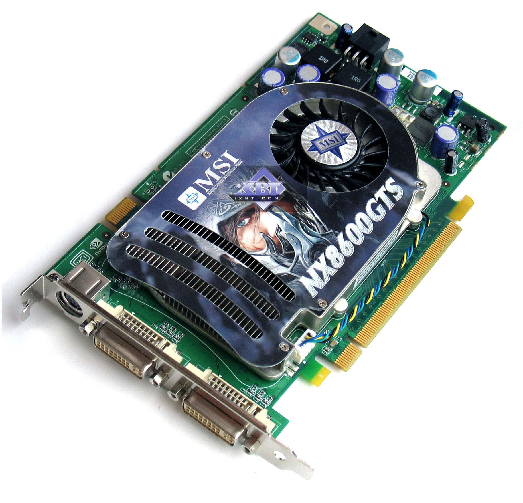
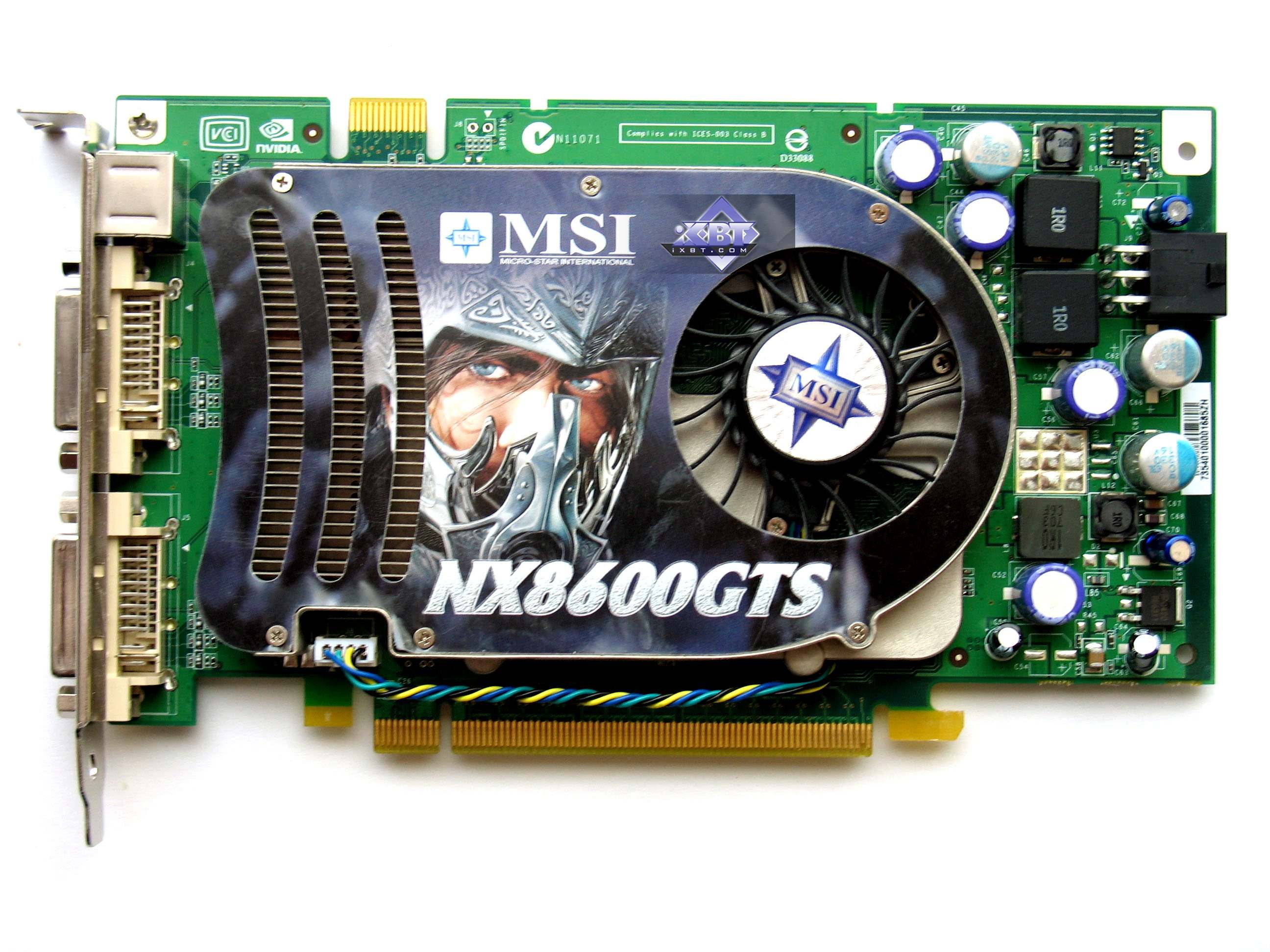
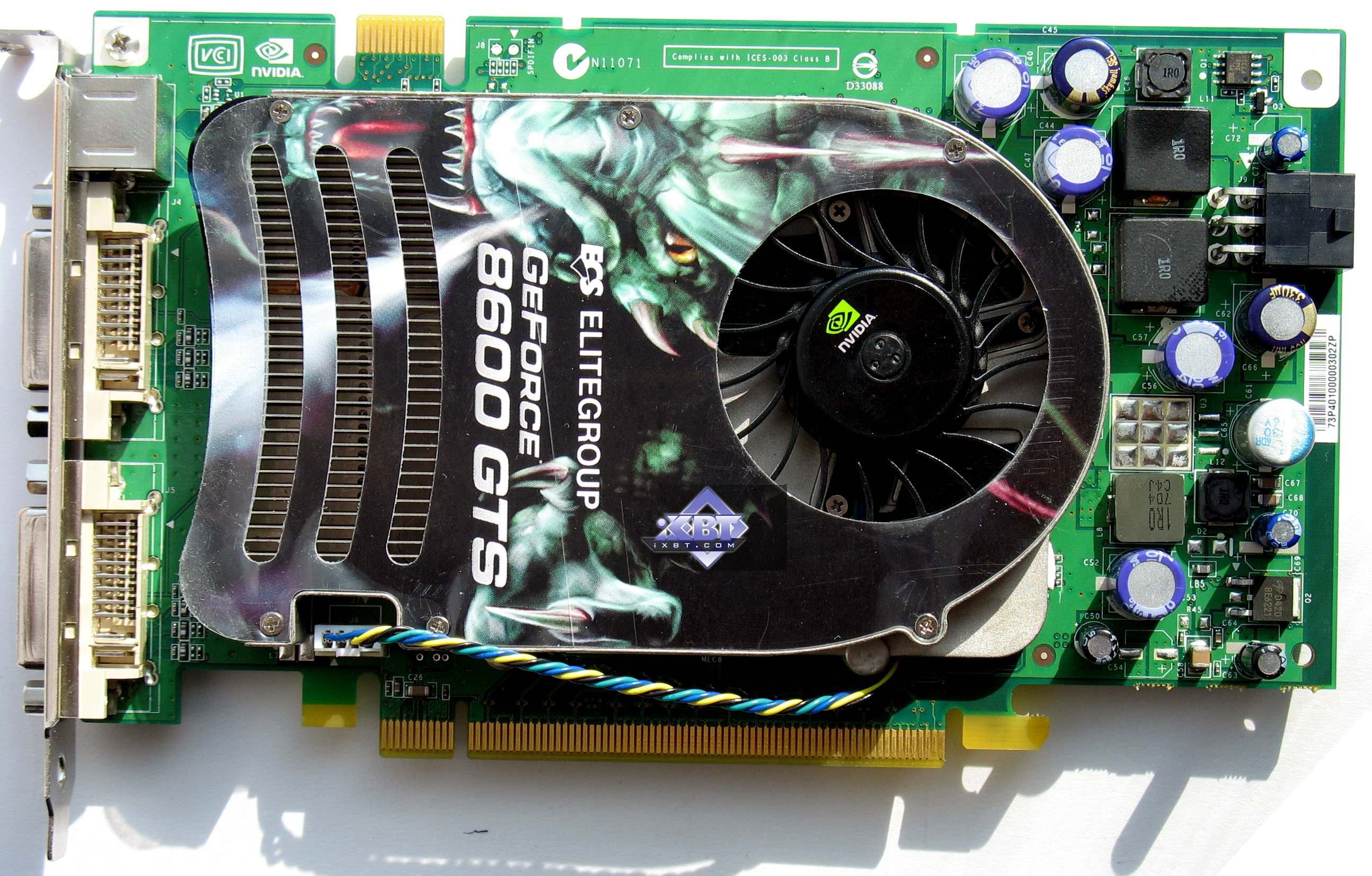
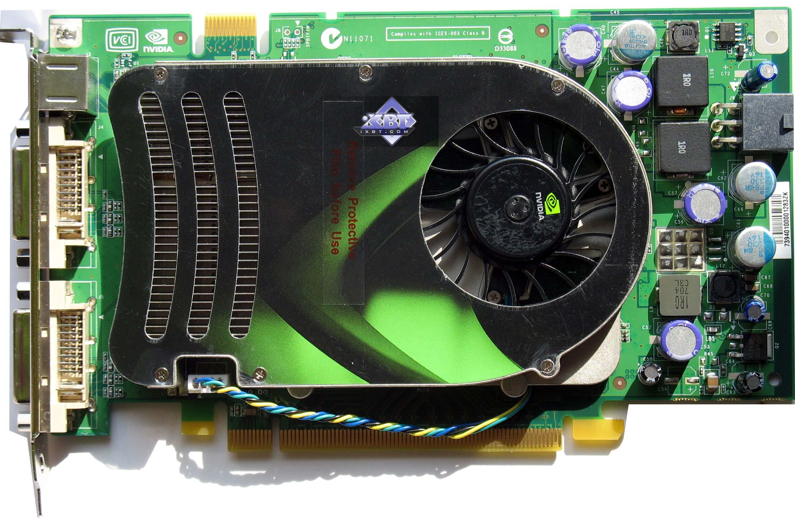
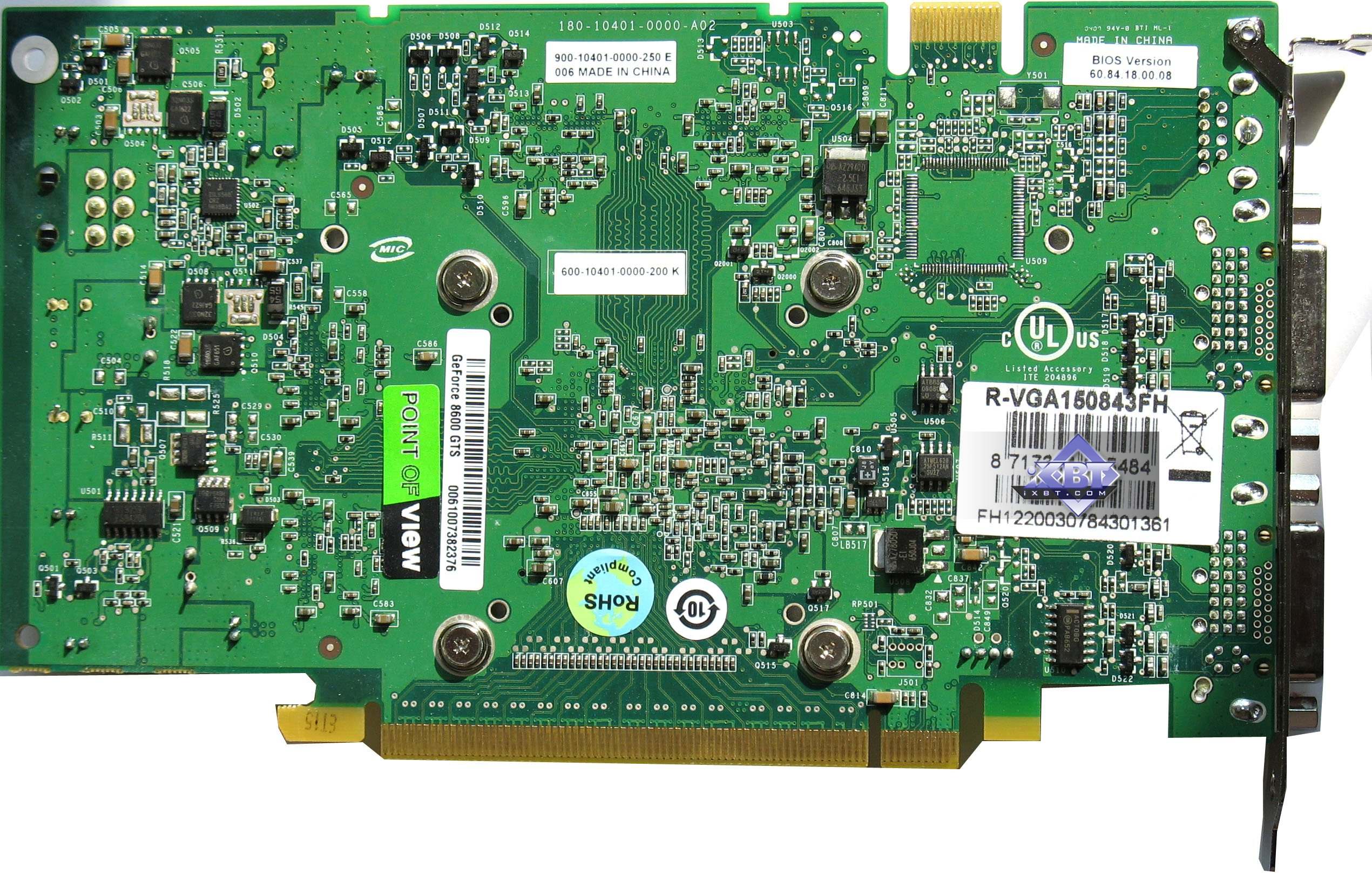
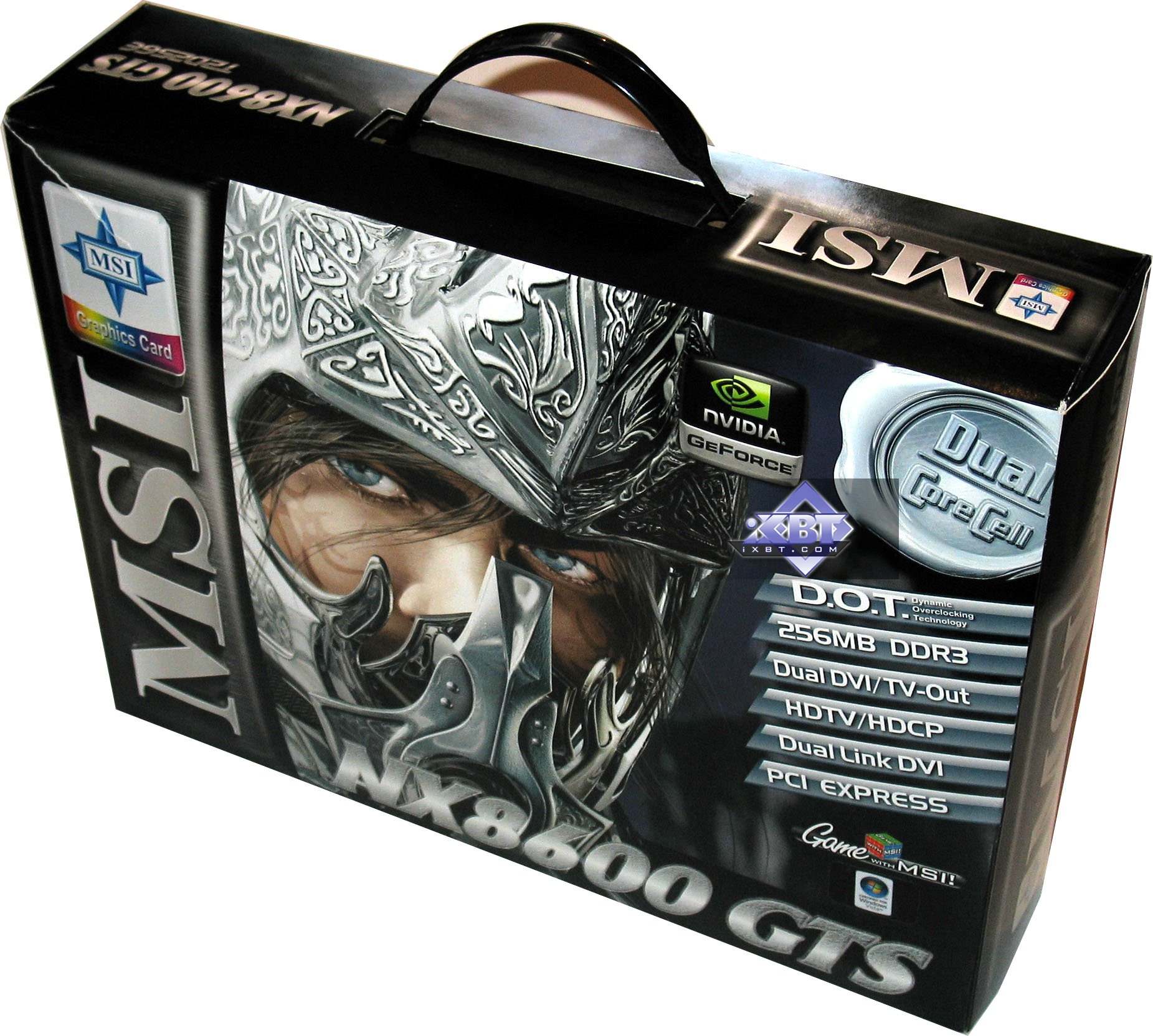
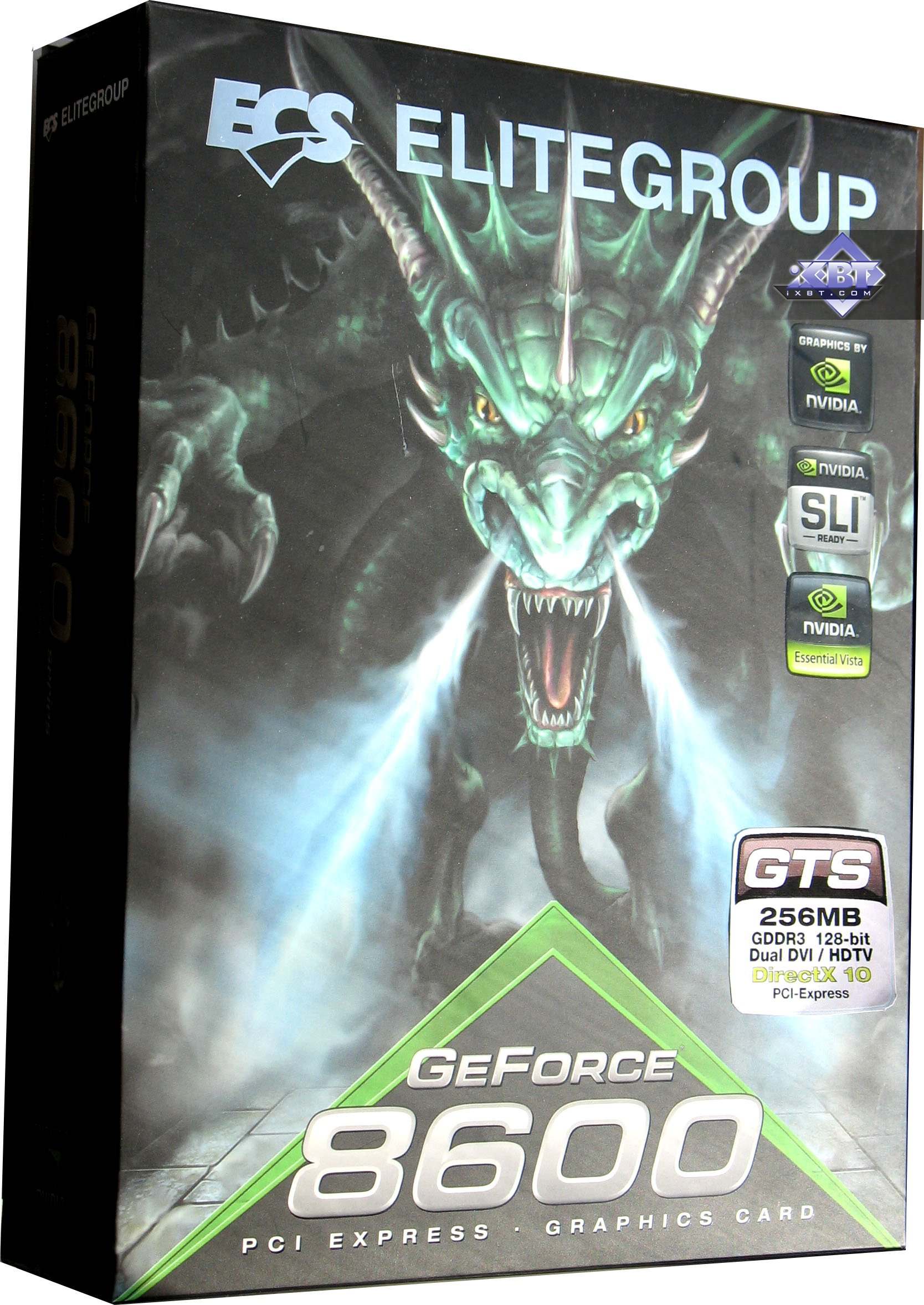
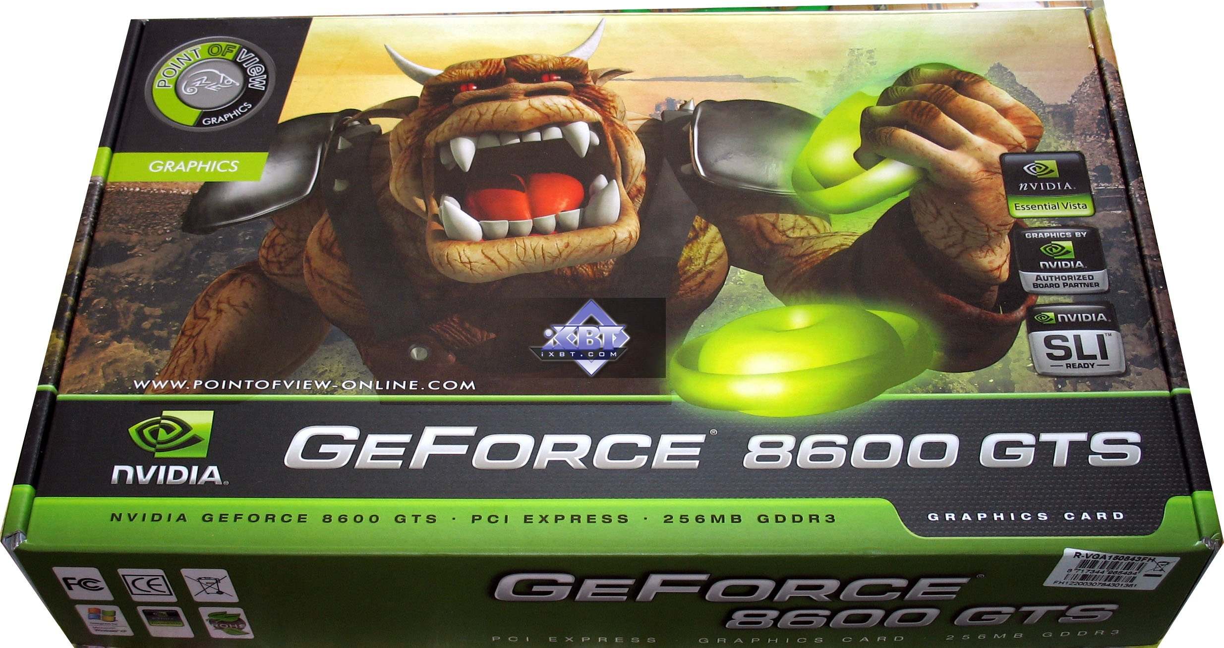
We've tested three video cards from MSI, ECS and Point Of View. Running a few steps forward, I can tell that they are all practically identical (reference cards), the differences come down to frequencies in some cards. We should also note that cards from MSI and ECS offer increased frequencies, although they are marked as regular, and MSI will have a special 8600 GTS OC card with increased frequencies. I wouldn't like to think that NVIDIA arranged press samples to work at higher frequencies than the future production-line cards. Or to make it impossible for any partner to present an overclocked card right after the announcement, to look better than competitors. This way or another, it does not look nice.
So you should keep in mind the following: production-line frequencies of the 8600 GTS are 675/2000 MHz. Only overclocked cards can offer higher frequencies... Drivers used in our tests did not allow to control frequencies. (Deliberately!) Fortunately, the author of RivaTuner, Alexei Nikolaychuk, added support for this card to his utility:
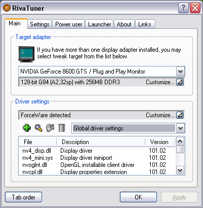
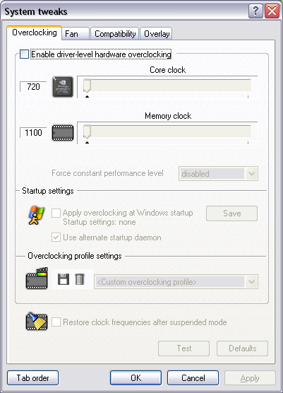 So we used it to reduce the frequencies to the reference level. Why? A video card with normal frequencies was the last to appear in our testlab, when we had already run all our tests. At increased frequencies, of course, and... That's a special case. Yep, we can use RivaTuner to reduce frequencies to 675/2000 MHz, but BIOS of the first cards operating at 725/2200 MHz is locked to a certain frequency proportion between ROP and Shader units. Namely, 1 to 2. That is when ROP operates at 725 MHz, the shader unit operates at 1450 MHz. Have a look at the specifications - this very frequency of the shader unit is necessary. But ROP should have operated at 675 MHz. And in our case it's 725 MHz. When ROP frequency is decreased to 675 MHz, shader frequency also drops to 1350 MHz. So we were about to publish results of these two cards for both frequencies and warn users that the real performance would lie somewhere within these limits. But fortunately, the problem was resolved, because there appeared a card operating at production-line frequencies - 675/1450/2000 MHz.
Video Cards
We can see well that the 8600 has a more complex design than the 7600 GT, because the core/memory kit requires additional power supply. It means that the power supply unit of the video card has been enlarged, which made the PCB bigger.
You can see on the photos that the card needs one 6-pin PCI-E cable from a PSU. You should keep it in mind. PSU requirements: you need a 350W (or higher) PSU with the 12V channel supporting at least 18-20A. The cards have TV-Out with a unique jack. You will need a special adapter (usually shipped with a card) to output video to a TV-set via S-Video or RCA. You can read about TV Out here. The cards are equipped with a couple of DVIs. They are Dual link DVI, to get 1600×1200 or higher resolutions via the digital channel. Analog monitors with d-Sub (VGA) interface are connected with special DVI-to-d-Sub adapters. Maximum resolutions and frequencies:
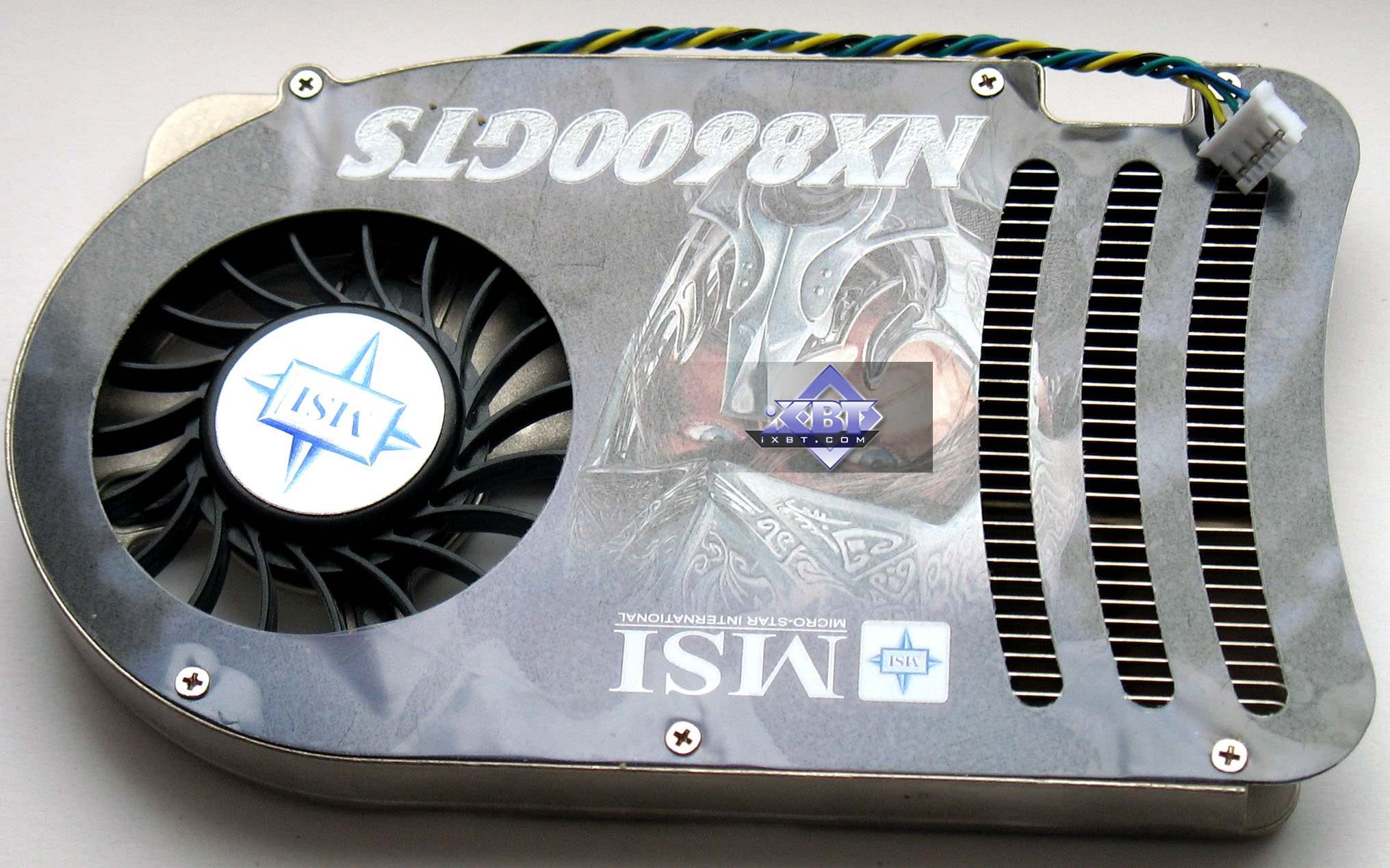
I remind you that only THESE two cards from MSI and ECS operate at 725/1450/2200 MHz. The same production-line models will operate at standard 675/1450/2000 MHz. Now what concerns the cooling system. As it's identical in all the three cards, we'll examine it in the MSI product:
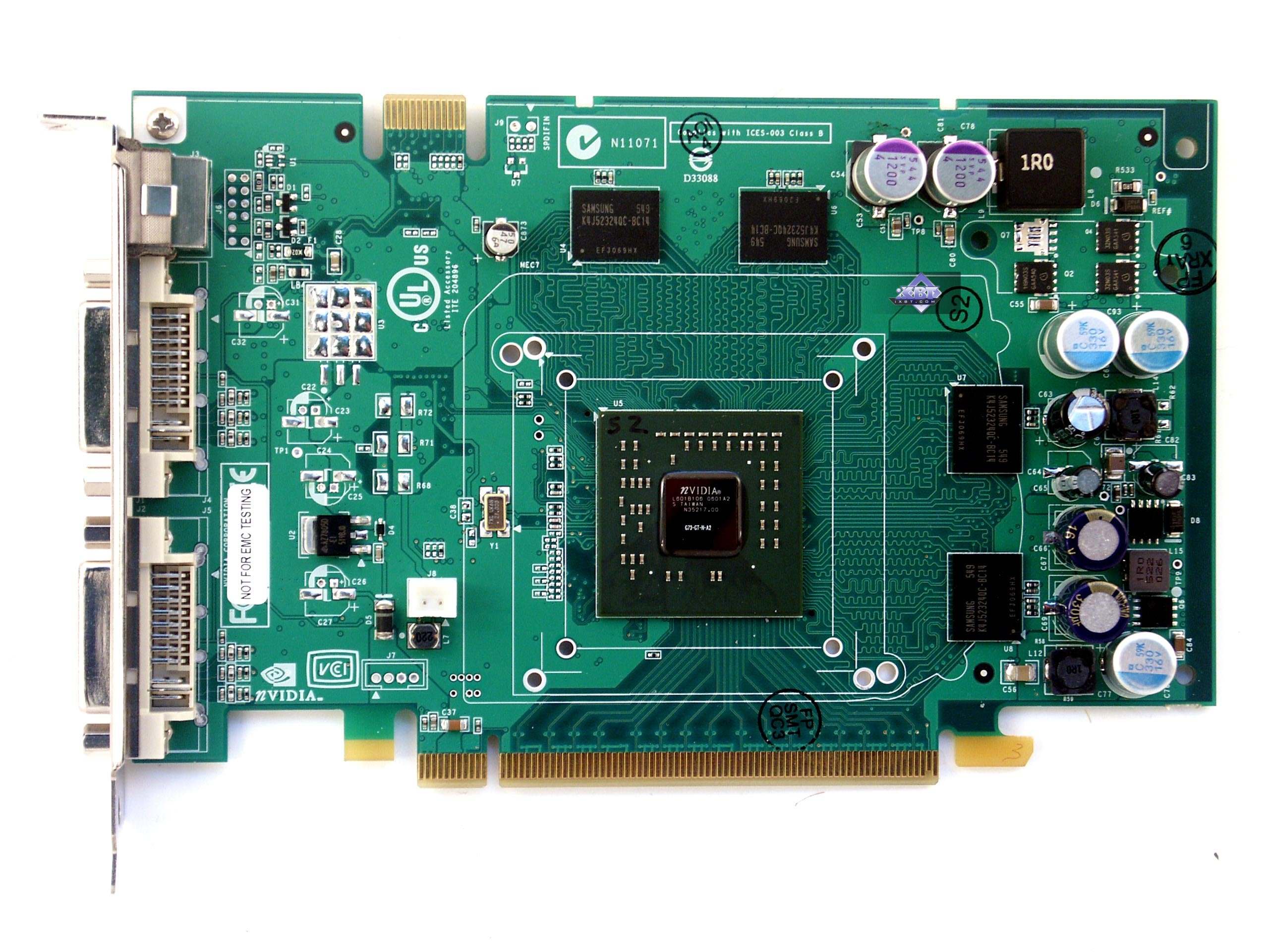
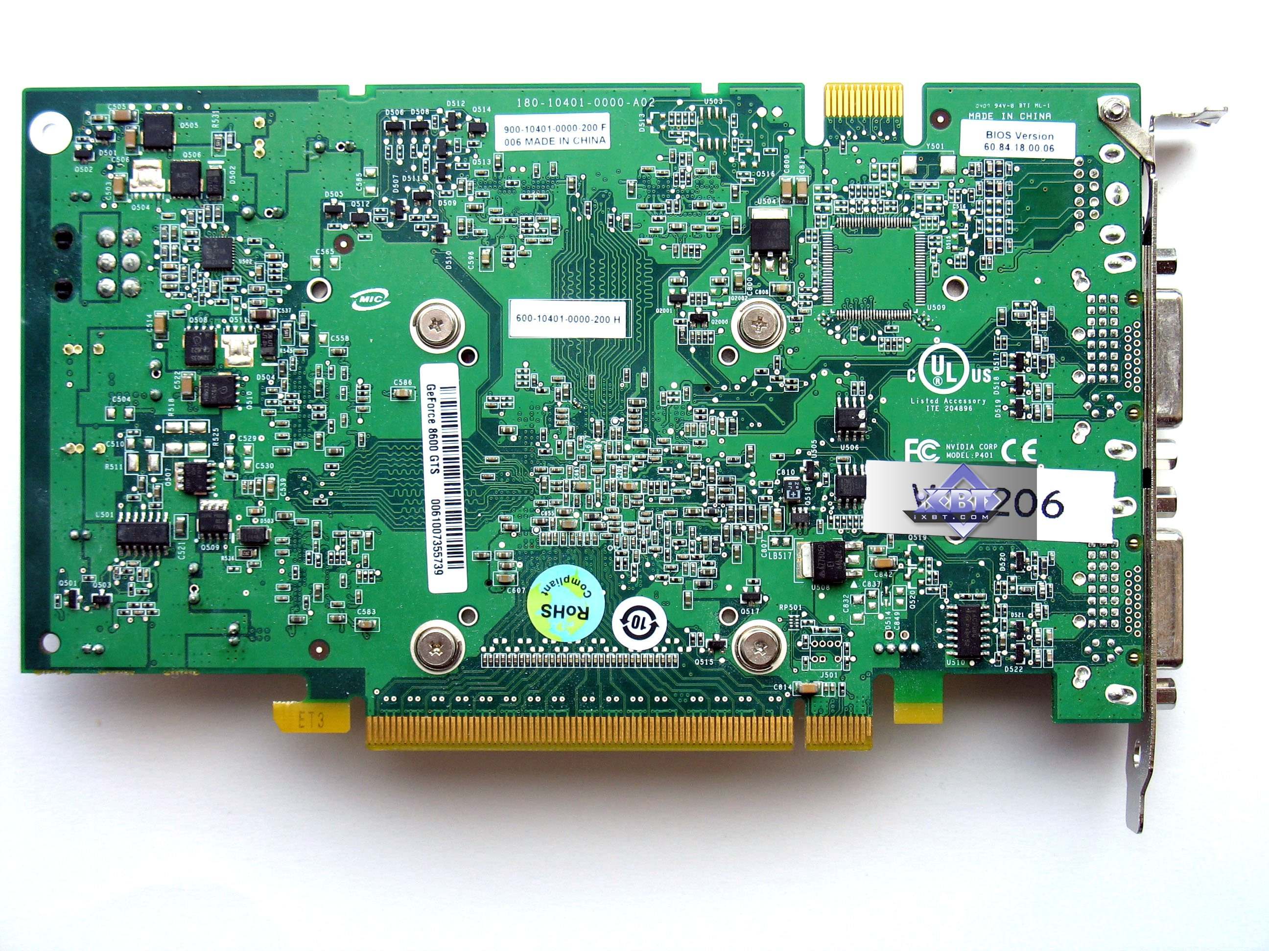
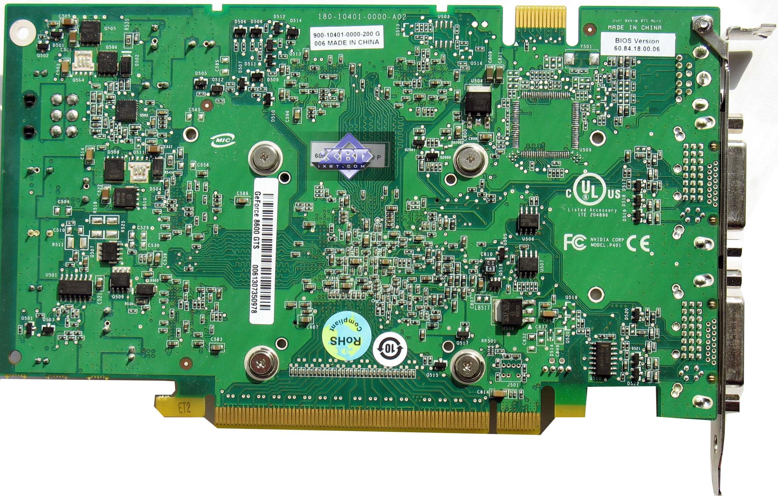
Now have a look at the processor. 8600 GTS — G84 is manufactured on Week 6, 2007. It's February, that is the GPU is just a tad older than 2 months
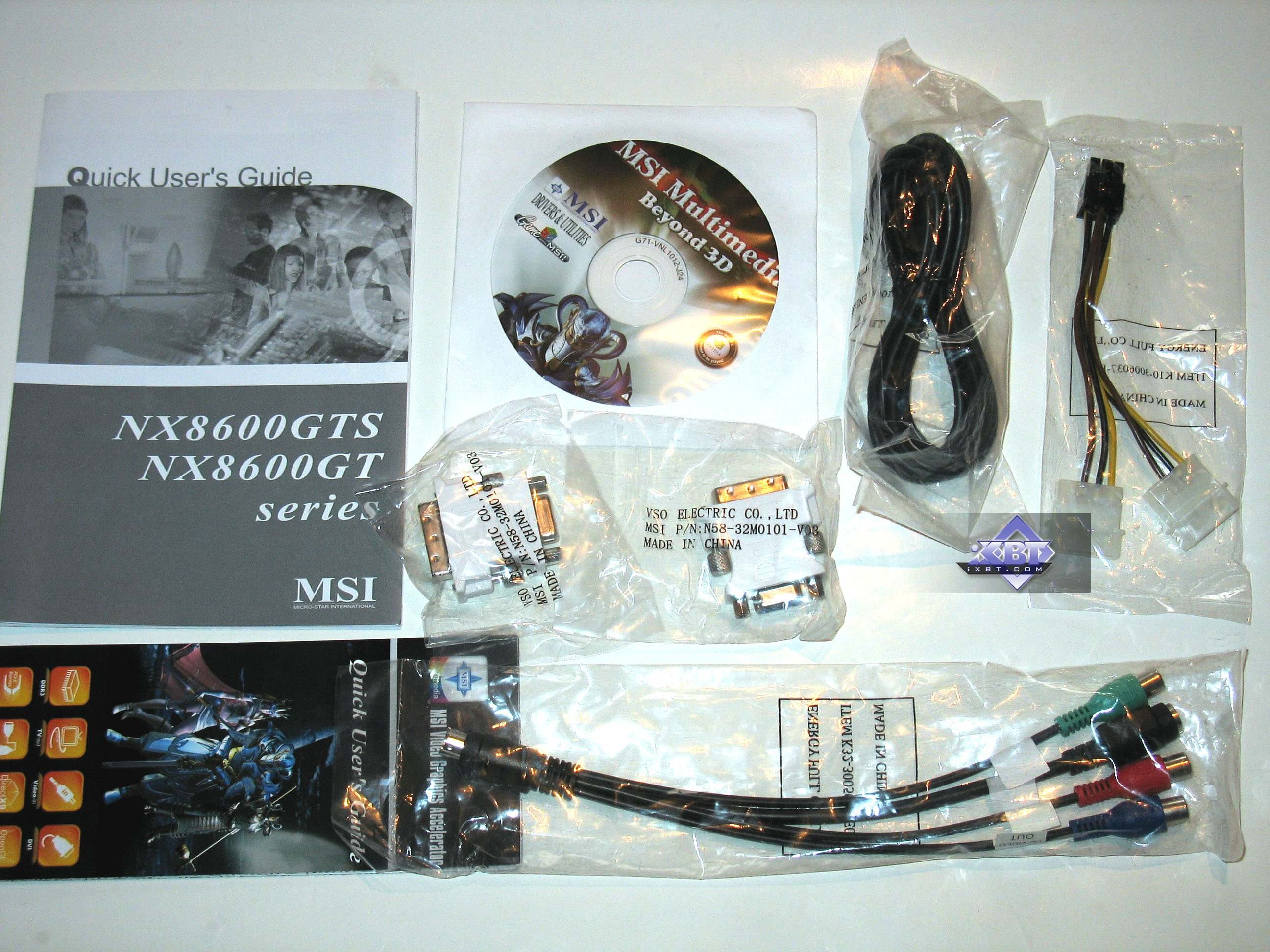
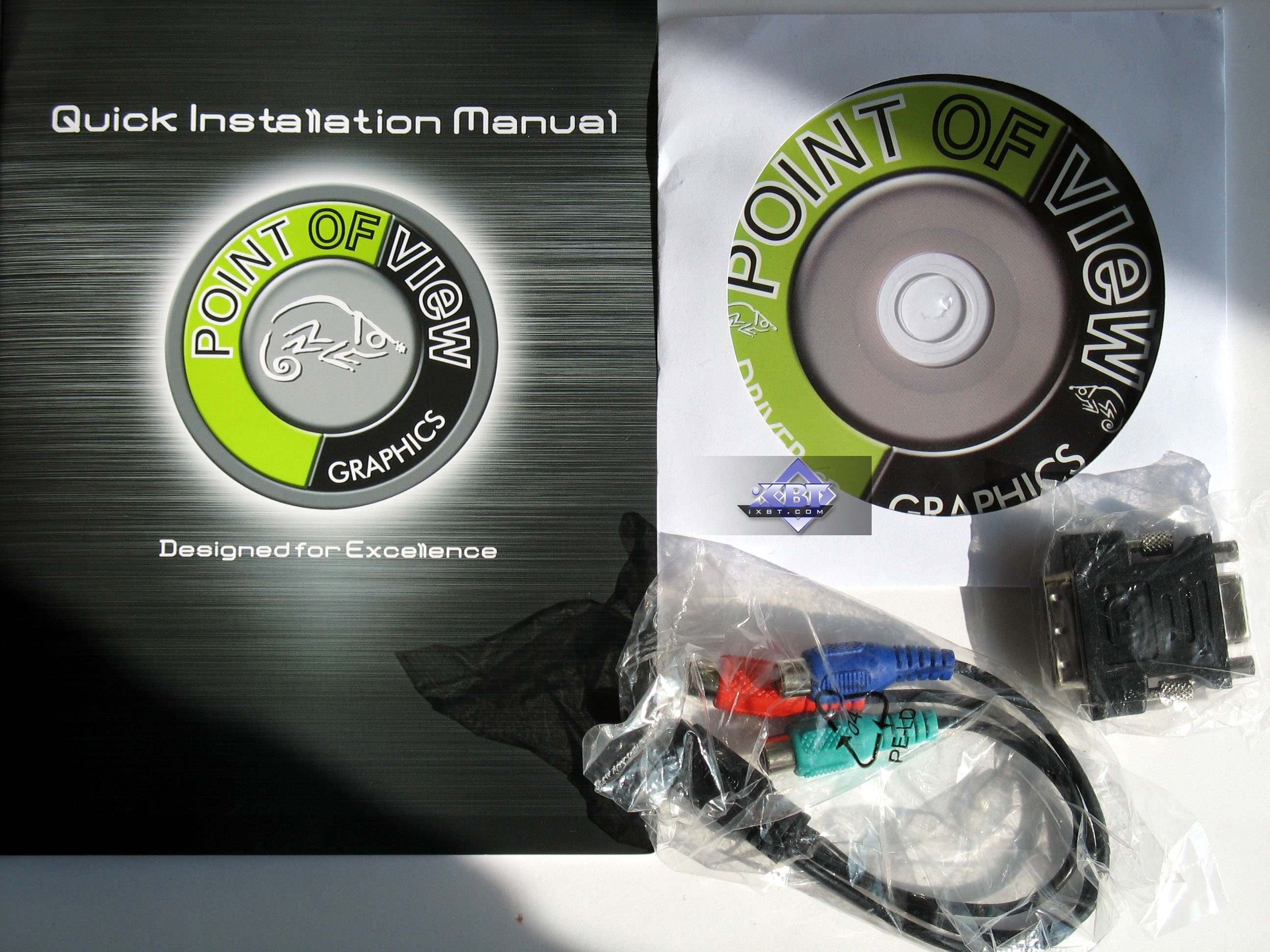
Bundle
Box.
Installation and DriversTestbed configuration:
VSync is disabled.
I should repeat that the latest RivaTuner beta, written by Alexei Nikolaychuk, now supports this accelerator.
NVIDIA GeForce 8600 GTS (G84) 256MB PCI-E
675/1450/2000 MHz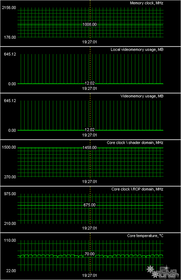 725/1450/2200 MHz The first screenshot shows how the card performs at the standard frequencies. We can see that maximal core temperature is quite low, but the cooler remains noisy (I don't understand why choose such a high rotational speed). The second screenshot shows operation of the card at increased frequencies, maximum core temperature is even a tad lower than in the previous case.
Synthetic testsD3D RightMark Beta 4 (1050) and its description (used in our tests) are available at http://3d.rightmark.org We also used more complex tests of pixel shaders 2.0 and 3.0 — D3D RightMark Pixel Shading 2 and D3D RightMark Pixel Shading 3 correspondingly. Some of the tasks that appeared in these tests are already used in real applications, the rest shall appear soon. These tests can be downloaded from here. We are planning to use updated D3D RightMark in the nearest future. It's developed to test Direct3D 10 compatible video cards in Windows Vista. The old tests in it will be rewritten for DX10, geometry shader tests will be added. We'll try to analyze results of the new tests in one of the future articles, probably the one devoted to DirectX 10 solutions from AMD. Synthetic tests were run on the following video cards:
There is a simple explanation to two results of GeForce 8600 GTS at different frequencies. The nominal GPU frequency in this model is 675 MHz and 1450 MHz for unified shader processors. But our sample operated at 725/1450 MHz. The sample with nominal frequencies appeared later, when all the work had been already done. To make the comparison well posed, we reduced GPU frequencies to 675/1350 MHz (the frequency ratio between core and unified processors is unchanged) and tested the card at this frequency as well. In order to evaluate performance of GeForce 8600 GTS at the nominal frequency, we should watch the fillrate results of G84(675). Synthetic tests that show performance of vertex and pixel shaders will be close to G84(720) results. One can make things easier and take average values, as the difference is not that big. Pixel Filling test
This test determines a peak texel rate in FFP mode for a various
number of textures applied to a single pixel: 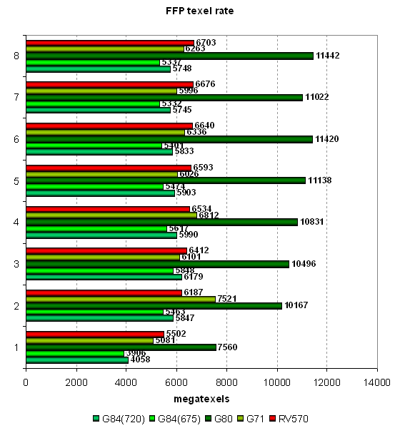 We can see well that 24 texture units in GeForce 8800 GTS are fast, high memory bandwidth does not limit performance, so the results are close to the theoretical maximum. RV570 is also very efficient, its sampling rate almost reaches the theoretical maximum. GeForce 7900 GS demonstrates worse results. It has 20 texture units, but their efficiency in synthetic tests is lower. What concerns the main hero of the review (G84), the peak sampling rate measured
in our tests does not confirm that its texture units can fetch 16
samples. Judging by our results, the chip can sample only 8 texels
per cycle (8 * 675 = 5400 mtex/s), not 16 (16 * 675 = 10800 mtex/s),
even though our tests use bilinear filtering, which theoretically
shouldn't affect performance. Either NVIDIA specs contain a mistake,
and the GPU actually has only 8 sampling units instead of 16, or the
drivers are too buggy — that's a great mystery so far. But the
fact is we cannot see the effect of 16 texture units. 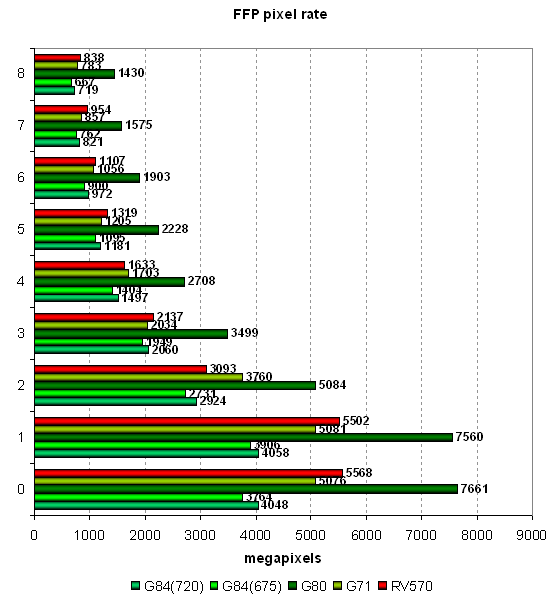 Our second fillrate test demonstrates a similar situation, but from the angle of pixels written into a frame buffer. In case of 0 and 1 texture, RV570 and G71 gain some advantage owing to higher bandwidth. Then the situation settles down. G80 shoots far forward with a lot of textures, and G84 is still almost twice as slow and competes with GPUs of the previous generation. Let's test the same task executed by Pixel Shader 2.0:  Nothing changed much. FFP and shaders operate on a par (probably FFP is emulated by an effective shader) and the cards demonstrate similar results. G84 slumps in the PS 2.0 test (compared to FFP) only in case of one and two textures — that's the only interesting result here. In fact, you should treat synthetic tests on a unified architecture with extreme care. They usually load certain parts of a chip, while real applications use all its resources. While a GPU of an old architecture can demonstrate peak performance in a well-balanced game, a unified GPU may yield worse results than in synthetic tests. It's was a foreword to geometry tests. Geometry Processing Speed test
First of all, let's analyze the simplest vertex shader that shows
maximum possible triangle bandwidth: 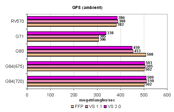 In the light of the above-said, no wonder that unified GPUs G80 and
G84 are leading. But their results are evidently limited by API and
platform resources, not by the speed of corresponding GPU units. On
the whole, GPUs offer similar execution efficiency in various modes,
peak performance in FFP, VS 1.1 and VS 2.0 is little different. Interestingly,
results of G84 in VS 1.1 and 2.0 are even higher than in G80 —
that's evidently the effect of badly tuned drivers. Let's see what
will change in a complex test with a single diffuse light source:
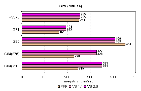 The layout of forces here starts to resemble the real situation, although G80 has not revealed its full potential yet. G84 is outperformed by the top solution here, but it's faster than traditional architectures - which is only natural. We are again surprised by relatively slow performance of FFP. Perhaps, driver optimizations are shifting towards programmability. We'll see what will happen in heavier conditions. The third diagram (GPS)
shows a more complex shader with a single light source and a specular
component: 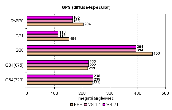 Now we can be sure that G80 is the evident leader in geometry performance. The unified architecture has fully revealed its potential, although G84 might have been faster. On the other hand, we can see well that 32 unified scalar processors are not enough, when 7-8 vector processors are dedicated to geometry. Interestingly, a mixed light source reveals optimized FFP emulation, which is available in all GPUs except G84. Let's analyze a still more complex geometry task that includes static and
dynamic branches: 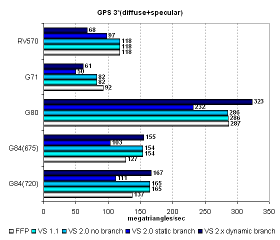 We've got a similar situation here. The unified architecture G8x reveals its force in synthetic tests. The more complex a task, the better results compared to traditional GPUs. G84's results are close to those demonstrated by G80, except for the difference in FFP emulation and dynamic branches, which are anomalously fast in G80. We can again see inverse weak spots of vertex units in the existing architectures from AMD(ATI) and NVIDIA — dynamic branches lead to a significant performance drop in GPUs from the former, while static branches slow down GPUs from the latter. Let's hope that the situation with "dynamics" will improve with the release of new unified GPUs from AMD. Let's draw a bottom line under geometry tests: G84 demonstrates unexpectedly strong results in synthetic geometry tests. Owing to its unified architecture, this GPU performs well in such lop-sided tests. It can use all 32 ALUs operating at high frequency to solve geometry. The unified architecture demonstrates excellent flexibility and capacities for complex vertex shaders. But let's see what happens in real games. The strength of the unified architecture is also its weakness — ALUs will mostly execute pixel shaders... Pixel Shaders Test
The first group of pixel shaders to be analyzed is very simple for
modern GPUs. It includes various versions of relatively simple pixel
programs: 1.1, 1.4, and 2.0. 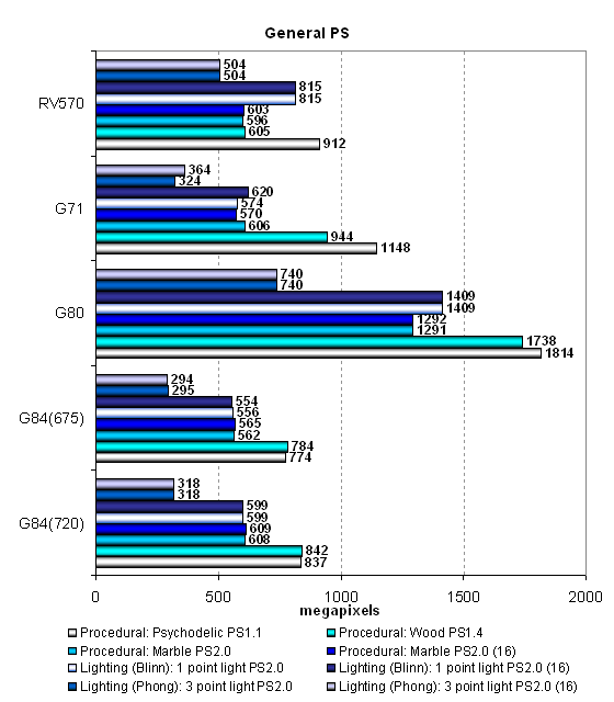 Here is the first alarm that indicates too few execution units in G84. Yes, GeForce 8600 GTS is approximately on a par with GeForce 7900 GS in most tests. But is it what users really expect from it? Even the competing solution of the previous generation outperforms the new cards in the most complex cases! G84 is more than twice as slow as the cheapest G80. It was to be expected judging by the number of unified processors and their operating frequency. Perhaps, these tests are too simple for G8x, and they cannot reveal full potential of the architecture. But the result put us on guard. By the way, shaders with reduced precision are executed faster on G71. NVIDIA's old architecture gains advantage of the reduced number and precision of temporal registers, while the new architecture computes FP32 just like FP16. Let's have a look at results of more complex pixel programs: 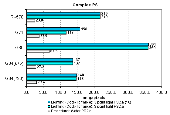 It's confirmed that the unified architecture G8x does not depend on precision, and results are identical for any precision. G84 is outperformed by G71 in the texturing-intensive procedural Water test (dependent sampling of nested textures), and it's on a par with G71 and heavily outperformed by RV570 in the compute-intensive test. What concerns G80, it's way ahead. It's another proof that no matter how wonderful a unified architecture is, insufficient number of ALUs has a strong negative effect on results. The situation may change in real applications, of course, but the overall tendency is noticeable: GeForce 8600 GTS is on a par with GeForce 7900 GS and RADEON X1950 PRO, nothing more. Of course, the new solutions support DirectX 10 and other features, but why forget about performance? Considering that the series offers nothing between GeForce 8600 GTS and GeForce 8800 GTS with 320 MB of memory, the performance gap between these solutions becomes obvious. They shouldn't have cut the new chips down so much or they should have offered still slower solutions based on G80. New Pixel Shaders testsThese new tests were introduced not long ago. We are planning to pay more attention to them. We are going to give up early synthetic tests with outdated shaders (lower than SM 2.0) and use SM 2.x, 3.0 and 4.0 written for HLSL. Performance of old shader versions can be benchmarked in games, where they have been used for a long time already. And synthetic tests must face the future. These tests are divided into two categories. We'll start with simple Shaders 2.0. There are two new tests, which implement effects that are already used in modern 3D applications:
Both shaders are tested in two modifications: arithmetic-intensive and texture
sampling intensive. We also test the difference for reduced and normal
precision. Let's analyze arithmetic-intensive modifications, they
are more promising from the point of view of future applications:
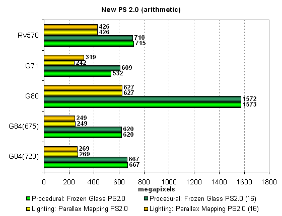 G84 results are not comforting again. The first place always belongs to G80, especially in the Frozen Glass test. Then follows RV570 with many pixel shader units (that's where we see benefits from the 3:1 proportion between pixel and texture units). G71 and G84 demonstrate very close results. We have an impression that NVIDIA deliberately made GeForce 8600 GTS perform on a par with GeForce 7900 GS. We are particularly disappointed with the results of G84 in parallax mapping... And now let's analyze the texturing-intensive modification of the same tests:
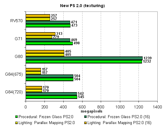 The situation is a little different here, it hasn't changed for the better for our contenders. Performance in tests is now limited by texturing units, so the AMD solution has come close to G71. G80 is traditionally way ahead. But G84 is now in a worse position, heavily outperformed by all cards in the parallax mapping test. We can see that G84 has no obvious strong sides, it has too few ALUs, and TMU capacities are rather weak. Unless it's intended to compete with the cut-down G71... We'll digress a little from G84. Let's remember the situation with the arithmetic and texturing preferences. These two diagrams show well that the arithmetic-intensive shader operates faster even on G71, the texturing-intensive modification makes no sense. The unified architecture of G8x evidently prefers computing to texturing. Much will depend on programmers' preferences as well. Arithmetic-intensive algorithms should be used to reveal full potential of the new chips. And now we'll analyze results of two more tests of Pixel Shaders 3.0, the most complex synthetic tests for the moment. D3D RightMark includes two shader programs - long, complex, lots of branches:
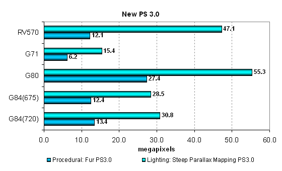 The load of these tests is worthy of G80, to say nothing of other solutions. The architecture of G8x evidently works better with dynamic branches in pixel shaders and is well suited for such tasks, especially compared to G7x. Although RV570 efficiently executes complex Pixel Shaders 3.0 with lots of branches. What concerns G84, it demonstrates good results in the Fur test, similar to RV570. But in the steep parallax mapping test it's outperformed by the GPU from AMD and defeats G71. Interestingly, the difference between G84 and G80 is smaller in these tests than in previous ones. Conclusions on pixel shader tests: G8x is a powerful computing system, of course. It's well suited to execute complex pixel shaders. The more computations in a task, the better. But the number of execution units and TMUs in the new Mid-End GPUs is too small, so they cannot outperform prev-gen cards in most tests. Most sorrowfully, G84 has few texture units as well as ALUs. The first fact does not allow the cards to demonstrate very good results in modern games, which still depend much on texturing performance. The second fact will not allow to succeed in games to appear in the nearest future. We'll see whether this assumption is confirmed in modern games in the next part of the article... Hidden Surface Removal test
Peak HSR performance (without/with texturing) depending on geometry
complexity: 
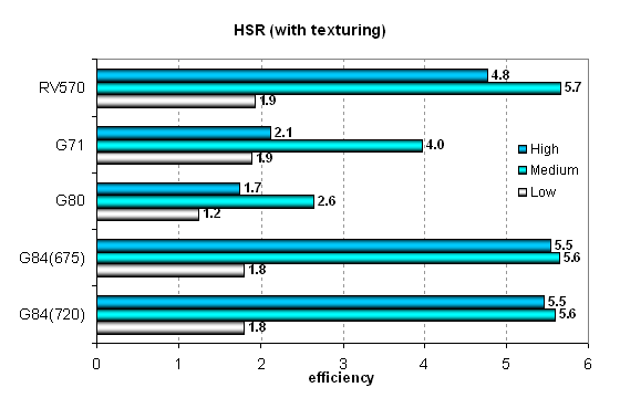 That's a nice surprise! It's actually the first significant change in behavior of the new solutions compared to G80. We can see well that G84 has much higher HSR efficiency than G80 and G71. Moreover, NVIDIA's GPU not just caught up with AMD's GPU (they have always been leading in these tests) in this parameter, but it demonstrates higher HSR efficiency in some cases. I wonder what has been changed in the GPU? Have they added hierarchical HSR from NVIDIA or some units in G80 did not work as they had been intended and were disabled? NVIDIA does not mention it in its articles. But we double checked the results — no mistakes. Compared to the previous GPUs, G84 works much better with complex scenes. Perhaps, the balance has been changed to comply with modern requirements to the increasing geometry complexity in games. Have a look at the absolute values obtained in HSR tests: 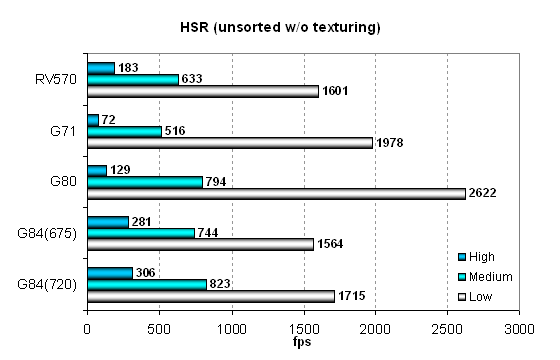
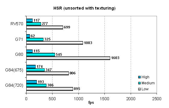 The results are very interesting! While G84 is outperformed in easy scenes by one or two prev-gen solutions, it already wins in scenes of medium geometry complexity, and it demonstrates absolutely the best results in the heaviest scenes - it even outperforms G80! We can see well that the balance has shifted to more complex geometry, which is good news. I think that NVIDIA made the right move. Of course, such complex scenes are not used in real applications so far, and G80 will often be the leader, even though it doesn't have the most efficient HSR. Point Sprites test
 Point sprites are used in a few real applications. We'll analyze their operation on various GPUs. Results of all our previous tests are confirmed — NVIDIA GPUs outperform AMD solutions with small sprites owing to more efficient operations with a frame buffer. As sprites grow in size and lighting becomes more complex, the latter starts to win. G84 performs like G80, corrected for frequencies and the number of units. So we'll see nothing interesting here. This test is limited only by the fillrate with small sprites. Conclusions on the synthetic tests
So, NVIDIA did well from the architectural point of view. It scales well both ways, it's unified, it's designed for complex shaders and other computations. But why did NVIDIA cut Mid- and Low-End solutions down so severely in execution units? There are evidently fewer ALUs and TMUs than expected. Can this potential mistake show up after competing solutions are launched? We'll analyze results of DirectX 10 tests and games, of course. Only they can show what the new GPUs are worth for, they can fully reveal potential of the new architecture. And now we are to analyze the situation in games and determine whether our synthetic conclusions are true. The next part will reveal all that remains hidden so far. In fact, it's the main part of the article, because users should make their choice on game results. NVIDIA GeForce 8600 GTS (G84). Part 3. Game tests (performance)
Andrey Vorobiev (anvakams@ixbt.com)
May 29, 2007 Write a comment below. No registration needed!
|
Platform · Video · Multimedia · Mobile · Other || About us & Privacy policy · Twitter · Facebook Copyright © Byrds Research & Publishing, Ltd., 1997–2011. All rights reserved. | ||||||||||||||||||||||||||||||||||||||||||||||||||||||||||||||||||||||||||||||||||||||||||||||||||||||||