 |
||
|
||
| ||
Part 2: Video cards' features, synthetic testsTABLE OF CONTENTS
NVIDIA GeForce 7900 GTX/GT (G71), GeForce 7600 GT (G73). Part 1. Theoretical materialsNVIDIA GeForce 7900 GTX/GT (G71), GeForce 7600 GT (G73). Part 2: Video cards' features and synthetic testsAll architectural peculiarities have been already described by Alexander Medvedev in the first part of the article. So, the new NVIDIA family currently consists of the following cards:
Note that the recommended price is always specified for the North American market, so you shouldn't expect such prices in Russia or Europe. You should take into account tax and customs specifics in a given country. That's why these prices are nothing more than a reference point. I guess that the 7900 GTX will appear in Russia for about $750, 7900 GT - for $450-$500, 7600 GT - for $250. Alas, that's specifics of the Russian market: the silliest new customs regulations (they seem to have been compiled by a person, who have never seen a video card, but who considers himself a specialist) as well as the desire of retailers to get super profits (however, the price is determined by the demand: if 7800 GTX 512MB cards were swept from the shelves for $850, why should retailers drop prices? - it's a logical move).
We got two bundles with such cards at NVIDIA Editor's Day (we'll describe it in Part IV of our review). The second bundle is to test the SLI mode. All the three product have different designs and different PCBs, so we shall thoroughly examine each of them. Video Cards
As you can see well on the photos, only the 7900 GTX design is actually a copy of the preceding 7800 GTX 512MB card. The other PCBs are unique. 7900 GT card has become more compact, it's simplified even compared to the 7800 GT PÑB. But the key issues, namely the layout of memory chips and the core is nearly the same. This PCB layout takes into account new memory form factors (136-pin chips instead of the old 144-pin ones). What concerns the 7600 GT, we can see that only the new memory chips affected the PCB layout. Everything else is practically unchanged. Note that the 7900 GTX card is equipped with excessively fast 1.1ns memory. 1.2ns would have been enough for 1600 MHz. But from the reliability point of view, this solution is probably justified. Besides, prices for these memory chips are similar. The cards have TV-Out with a unique jack. You will need a special adapter to output video to TV both through S-Video as well as RCA (usually shipped with the bundle). It also allows Video-In to convert analog video stream into digital form (If you have it. Unfortunately, Philips 7115 codec was installed on only one card - 7600 GT). You can read about Video-In in more detail here. TV-Out details are published here. We can see that all the three cards are equipped with a couple of DVI jacks. They are Dual link DVIs (except for 7600 GT), which allow resolutions above 1600õ1200 via the digital channel. Analog monitors with d-Sub (VGA) interface are connected with special DVI-to-d-Sub adapters. Maximum resolutions and frequencies:
We should mention core frequencies separately. Nearly all previously reviewed GT/GTX cards allow to specify all the three core frequencies at 27 MHz steps and the geometry unit frequency was always higher by 40 MHz. We already wrote about it in detail before. But in this case the 40 MHz difference was removed from the 7600 GT card as well as the 27 MHz step. Now all the three frequencies can be changed at 1-2 MHz steps. All the frequencies are the same in the 7600 GT card and change synchronously. But in the 7900 GTX card the difference between the geometry unit frequency and the other frequencies of the core has even grown to 50 MHz. The 27 MHz step has been also removed. This difference in the 7900 GT card is 20 MHz, there is also no 27 MHz step. That's why the above mentioned core frequencies are real, they do not come down to one of the values from the row 432-459-486-513 MHz.
Now let's have a look at the processors.
Here it is, the intrigue of the day! Just have a look! The surface area of the G71 die has been significantly reduced relative to the G70! We calculated that the reduction amounts to 1.44 times! Besides, we already know that the number of transistors in a core has been reduced from 305 to 279 mln. NVIDIA experts designed the new chip well. As a result, we got just as efficient chip, operating at a higher frequency. But the die is very cheap and consumes very little power.
I guess there is no point in describing this GPU, as it's a copy of the previous model. That's actually the same chip, but operating at lower frequencies. It's crystal clear that the company will use 7900 GTX rejects (frequencies) for this chip.
Even though G73 has 12 pixel pipelines and 5 vertex pipelines versus 8 pixel and 3 vertex pipelines in the 6600 GT, the surface area of the core got smaller due to a thinner process technology and good design. Moreover, GPU operates at much higher frequencies relative to the 6600 GT. Using the new beta of RivaTuner we found out that G73 contains four quads instead of three (16 pipelines)! One quad is just disabled (locked on the hardware level and cannot be unlocked). It all means that in future we may see something like 7600 GTX with 16 pixel pipelines, as the process technology is streamlined. In that case there will rise a question whether the memory bandwidth is sufficient for this core (the bus is 128-bit). But first of all, it's just an assumption, such GPU may be never launched; secondly, as memory prices go down, these cards may be equipped with the fastest memory, which will make up for the narrow bus; thirdly, there appear new games, which require GPU performance in the first place, not memory bandwidth; fourthly, there is some chance that designers made a mistake in registers and that's why the program detects an extra quad, which does not exist (that's not likely, but to err is human).
Installation and DriversTestbed configuration:
VSync is disabled. To evaluate efficiency of the new core, we have also run tests on the 7900 GTX card at reduced frequencies to the 7800 GTX 512 level (550/1700 MHz). As I have already noted above, the latest beta version of RivaTuner (written by A.Nikolaychuk) supports these three products.
NVIDIA GeForce 7900 GTX 512MB PCI-E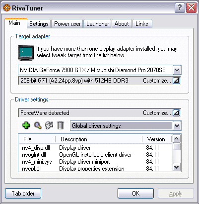 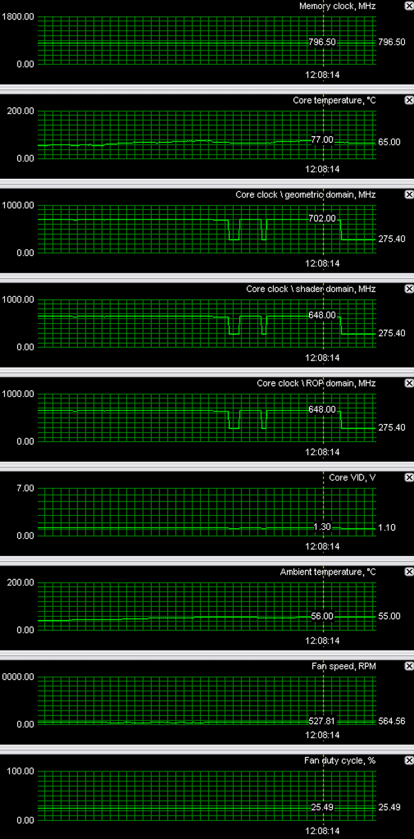 Note that we used RivaTuner to set the low rotational speed of the cooler to 25% of the nominal! The core temperature under load never exceeded 70°C at only 500 rpms! An excellent result! In fact, the card feels much cooler compared to 7800 GTX (the card is just warm - when you switch the computer off, you can easily remove it without burning your hands).
NVIDIA GeForce 7900 GT 256MB PCI-E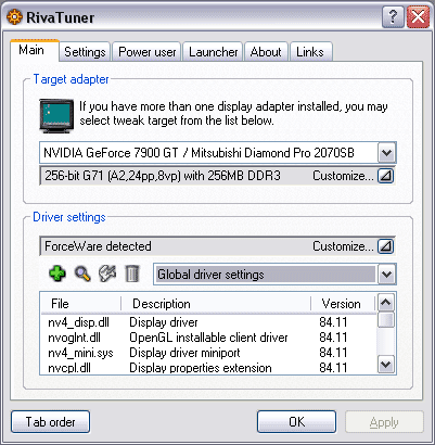 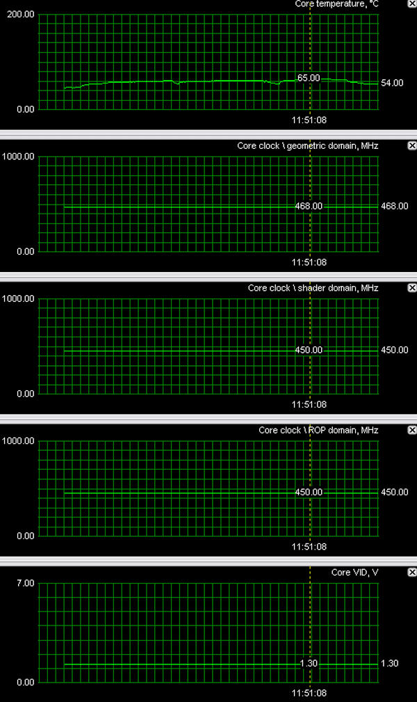 Unfortunately, the rotational speed of the fan is not detected by the monitoring chip, so we cannot publish the results. As we can see, the temperature under load even with such a small cooler (compared to the one on 7800 GTX; it's actually the same device, only modified a little) does not exceed 65°C (the fan speed is not high, so there is no noise).
NVIDIA GeForce 7600 GT 256MB PCI-E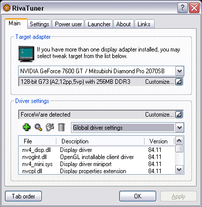 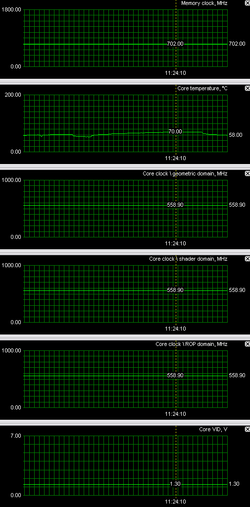 The situation with monitoring is the same here, but the cooler starts rotating much faster, when a 3D application is started. As I have already said, that's not a problem. RivaTuner can set the rotational speed down to 25% of the nominal value to stop the noise. Even in this case the core temperature does not exceed 70°C (we took the readings when the fan speed was limited to 25% of its maximum).
In the beginning of this part I wrote that we got two bundles. That's why we could analyze SLI mode in each card.
Synthetic tests
D3D RightMark Beta 4 (1050) and its description (used in our tests) are available at http://3d.rightmark.org
We also used new, complex tests of Pixel Shaders 2.0 that are adequate to present-day tasks - D3D RightMark Pixel Shading 2 and D3D RightMark Pixel Shading 3 tests, intended for the future. Now these tests are in beta stage and available to download here: We tested the following High-End cards:
Middle-End cards:
Pixel Filling test
Peak texelrate, FFP mode, various numbers of textures applied to a single pixel:
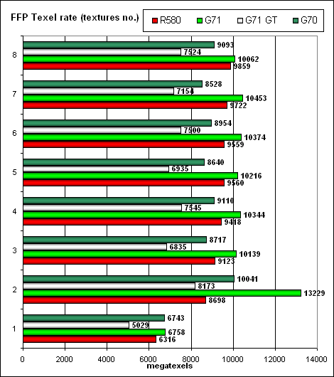
While the increased frequency of the core in the new G70-based card allowed us to speak of parity, the G71 is certainly a new leader. In this test. There are no innovations concerning mutual behaviour of ATI and NVIDIA or hints at architectural changes of G71 versus G70 (we have tested these chips at the same frequency and have found out that they are completely identical in everything, except for geometry performance; but it can be easily explained - a small difference in geometry unit frequencies between G71 and G70, all other frequencies being equal). So, there are no architectural differences, but the difference in the clock frequency makes the new chip a true leader. 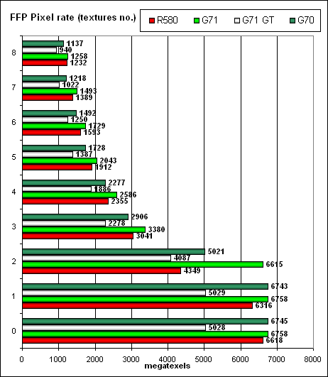 The same situation here, but in terms of the number of pixels written into a frame buffer. In peak cases – 0, 1, and 2 textures, G71 shoots forward.
Let's run the same task with PS 2.0:
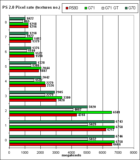 So we can establish a fact that nothing has changed — FFP as well as shaders operate in the same way (in terms of hardware FFP is emulated by a shader) and demonstrate the same results. Higher clock frequency of the G70 makes it dominant. Now let's have a look at the situation in the Middle-End segment: 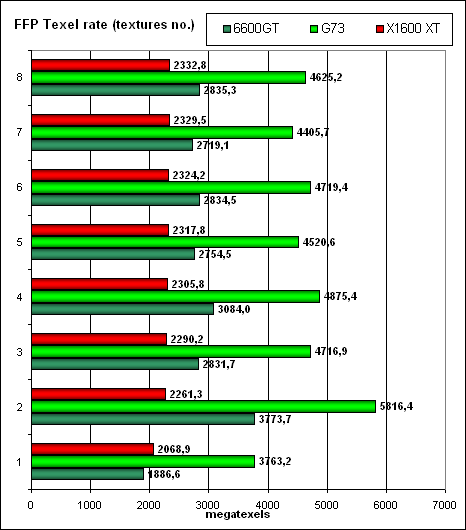 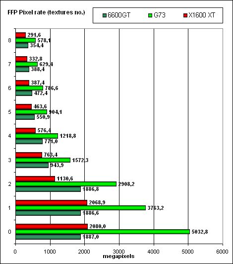 NVIDIA is doing even better in this segment, the new Middle-End hero (G73) is just beyond competition. Two-fold advantage without exceptions, that's great! ATI will be in difficult straits - R520- or R580-based solutions in this price segment will look awkward and will not bring much profit. Besides, we can see that RV530 competitiveness is dubious (we shall analyze this situation below). Geometry Processing Speed test
The simplest shader — maximum bandwidth in terms of triangles:

Everything is according to clock frequencies and a number of vertex units. R580 still leads in peak memory bandwidth. But as we know, it is not critical in modern games. Let's proceed to a more complex shader — a single mixed-light source:
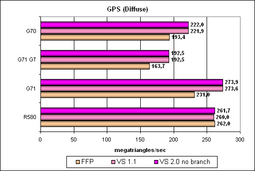
Tendencies are the same, but the increased frequencies of the G71 allow us to speak of parity. Let's complicate the task:
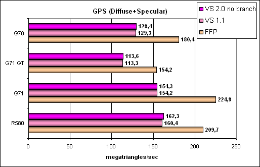 Hardware optimization of FFP emulation makes itself felt in case of a mixed light source – both NVIDIA and ATI offer this feature in the current generation of their chips. The cards fair strictly according to their frequencies. We can see that vertex architecture of the G71 suffered no changes, but the vertex unit offers higher performance. It's parity again. It's a more complex task, including branches: 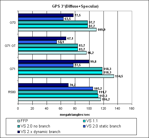 Here we can see again that branching is a weak spot of the ATI vertex unit. Together with the increased G71 core frequency, it's a no win situation on the verge of parity. High memory bandwidth for triangles does not save ATI in complex vertex tests. As in case with the G70, G71 prefers dynamic branching to static. Conclusions on geometry tests: the situation has not changed much on the qualitative level, but the quantitative difference between G71 and G70 brings to naught all R580 advantages, which we could mention in the previous comparison. We can see no architectural innovations or changes. Everything is just the same, but you'd better remember the epigraph to Part I. And now what concerns Middle-End: 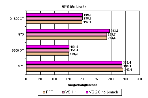 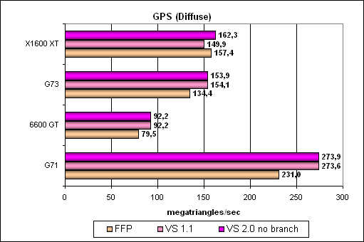 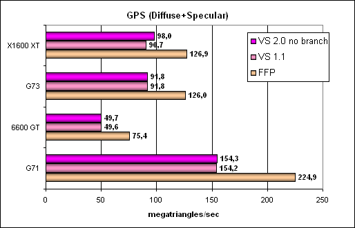 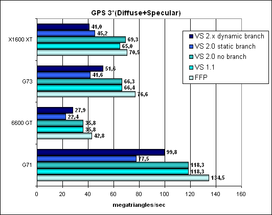 On the whole we can speak of parity between G73 and X1600 (RV530). G73 is the leader in absolute triangle memory bandwidth, but the other tests demonstrate stable parity. All our considerations about the architectural features remain true - RV530 and G73 units are inherited from top models. Just note that geometry performance in the Middle-End sector has even less effect on the results of real game tests - 128 bit memory buses make themselves felt and often act as rendering bottlenecks. G73 gains twice as much as NV43 - this chip was noticeably outperformed by ATI. Now the parity is restored. This fact will affect professional video cards (a traditionally successful domain for NVIDIA) based on G73 - geometrical performance is very important there. Pixel Shaders Test
The first group of shaders, which is rather simple to execute in real time, 1.1, 1.4, and 2.0:
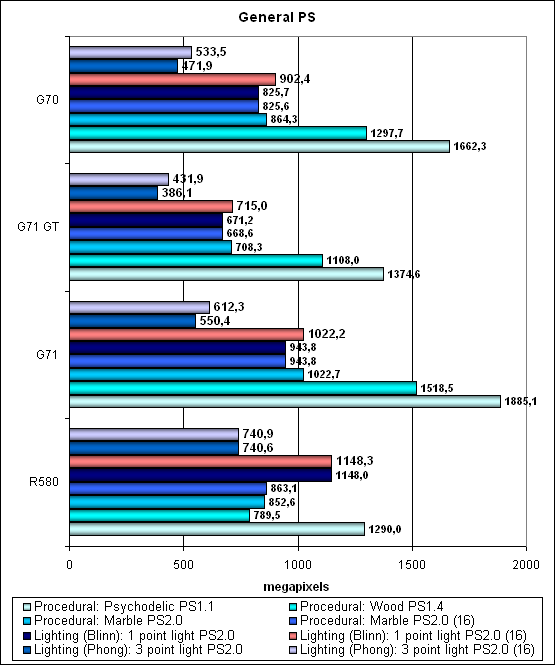 The situation hasn't changed versus the previous X1900 review - G71 just became a tad faster according to the increased clock frequency.
Let's have a look at longer shaders:
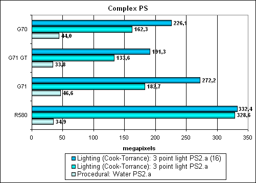 This situation again repeats the previous review - NVIDIA gains an advantage due to 16 bit precision (don't forget that intensive intermediate computations of this precision may result in noticeable deterioration of rendering performance; the current standard de facto and requirement to all future APIs is internal computations in FP32 format). R580 noticeably outperforms NVIDIA in complex PS, especially if we don't take FP16 results into account. That's laudable. Anyway, the layout of forces in pixel shader domain hasn't changed, everything will be up to applications. R580 is indeed a shader king and still outperforms G71 in many computations, which are not limited by texture sampling.
And now what concerns Middle-End:
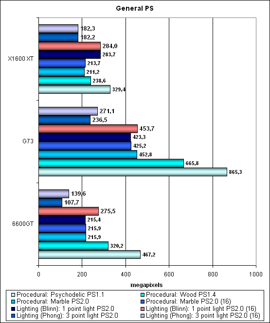 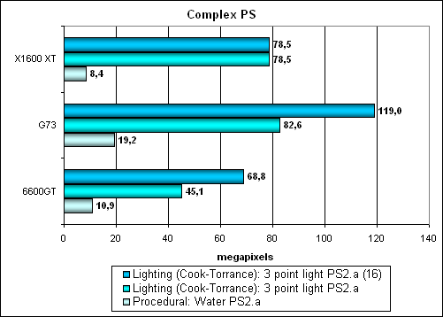 Despite the advanced X1600 architecture, 12 STERLING (unlike RV530) G73 pipelines make themselves felt. It's obviously superior to its competitor. The advantage varies from noticeable to considerable depending on a test. While ATI can challenge the GeForce 6600 series, it will be very hard to cope with G73. The company again faces the unfavorable question about cheap modifications based on R520 or R580. It's already clear that G73 is sort of a local sensation - it's stable, inexpensive, and very good! It's so good that it is unchallenged in this price segment, we cannot even compare it to any other card. To all appearances, real applications will only back up this conclusion. Our new shader testsThe new tests, which will gradually replace the old ones in our future reviews, can be downloaded (see above) as part of the archive with D3D RightMark beta. In future we are going to give up synthetic tests with earlier SM models and we shall focus on HLSL shaders for SM 2.0 and 3.0. Older shaders can be tested in existing applications, while synthetic tests (intended for the present-day situation or even for the future) must be adjusted to the spirit of the times - that's what we have done. Let's start with simple PS 2.0. There are two new tests with topical effects:
We test both shaders in two modifications: maximum priority to arithmetic and texture sampling. Besides, we check the results for FP16 and for FP32.
Here is the arithmetic-intensive modification of the task:
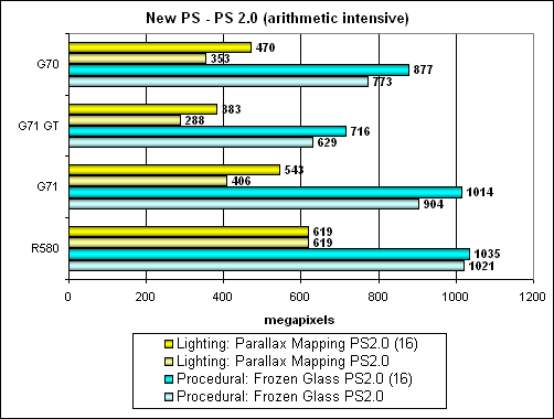
As we can see, R580 is a steady leader (it's especially good at parallax mapping), followed by G71. G71 performance noticeably depends on precision. We detected no architectural differences from G70. And now a texturing intensive modification of the same tests:
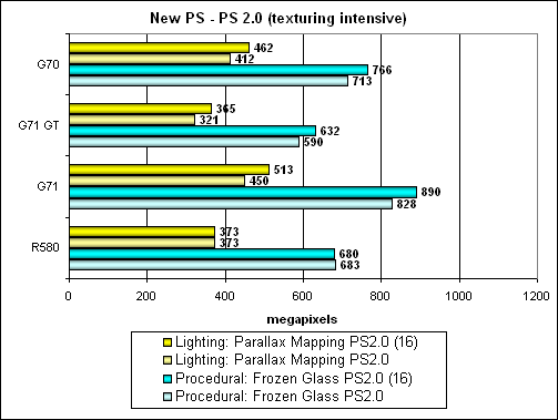 R580 advantage comes to naught here. It's an interesting situation – too much depends on context and programmers' preferences. We'll see what ways they will follow in their applications.
Conclusions: the increased clock makes itself felt, but the situation is still dubious, ATI's advantage in some cases is high. That's an evident reserve for the future – for complex cinematic shaders and an excellent head start for modern state-of-the-art games. But will it be used – the number of texture units in the R580 is still 16. In our game tests we shall see how modern applications feel about the 3:1 ratio, adopted by ATI, and how successful the increased G71 frequencies are at bringing this architectural advantage to naught in real games. HSR test
Peak efficiency (with and without textures) depending on geometry complexity:
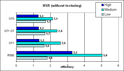 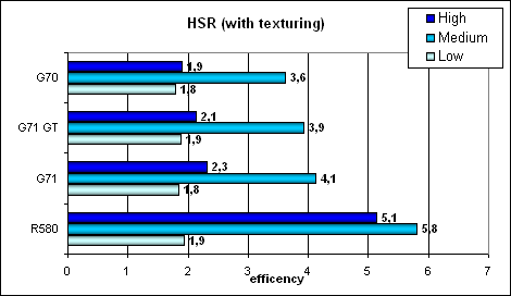 As we can see, there are no changes in the layout of forces. Hierarchical HSR from ATI looks better than a single-level HSR from NVIDIA, especially in complex and average scenes. NVIDIA rights itself in texturing thanks to more efficient (for simple fill) integration of texture units into the pixel pipeline.
And now what concerns Middle-End:
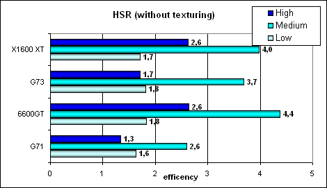  Despite the potentially lower architectural HSR efficiency, G73 can fight back. That's an evident parity with ATI. Interestingly, HSR efficiency is higher in Middle-End solutions from NVIDIA (NV43 and G73) versus High-End G71. But that's natural - scenes with lower resolutions and the same geometry complexity are typical of Middle-End, sparing memory bandwidth is very important here (HSR plays its role too). Point Sprites test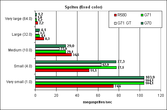 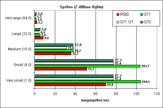 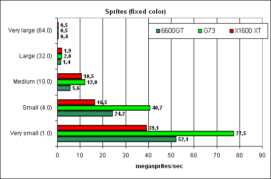 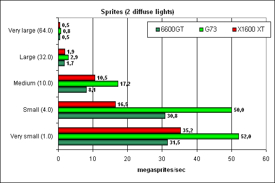 The data are published for High-End and Middle-End cards. Everything is as usual – NVIDIA leads with small sprites thanks to more efficient frame buffer operations. In case of High-End cards, it starts losing ground as sprites grow larger and lighting becomes more complex. But not fatally. In Middle-End segment G73 presses ATI. Just look, it's an obvious leader here. Conclusions on the synthetic tests
The next part is the most important - game tests. Read on! NVIDIA GeForce 7900 GTX/GT (G71), GeForce 7600 GT (G73). Part 3: Game tests (performance)Write a comment below. No registration needed!
|
Platform · Video · Multimedia · Mobile · Other || About us & Privacy policy · Twitter · Facebook Copyright © Byrds Research & Publishing, Ltd., 1997–2011. All rights reserved. | |||||||||||||||||||||||||||||||||||||||||||||||