 |
||
|
||
| ||
|
||
|
||
| ||
Part 1. Theory and architectureThe more transistors per pixel,
The more anisotropic and antialiased it is G71 - everything is the same, but noticeably better (to be tested in this article). 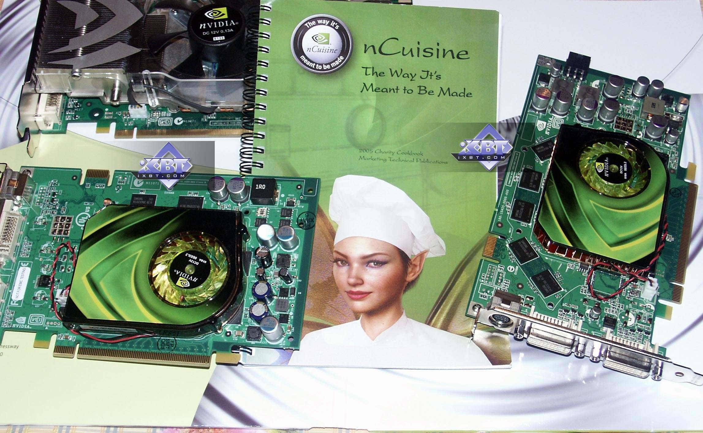
Microsoft Windows Vista is round the corner, it will bring new 3D technologies. But it will happen in over six months and companies carry on streamlining new process technologies, reducing, refining, and optimizing their profits. Faster, better, cheaper - sounds like an Olympic motto. ATI did well, when it upgraded its process technology from 0.15 micron to 0.13 low-k. The new products (RADEON X800 (R420)) offered very good characteristics, first of all in power consumption relative to their competitors. But starting from 0.11 microns, the Canadian company suffered a failure after failure. In the final analysis, R430 turned out a failure and was discontinued (speaking of top products). ATI didn't manage to launch a top product by the 0.11 process technology. Upgrading to 0.09 micron was even more painful. R520 was delayed for several months, which allowed NVIDIA (who also switched to the same 0.11 micron process technology) to outscore its competitor by launching G70 (7800 GTX). As we have already seen, the top accelerator from ATI (X1900 XTX), which was launched not long ago, gets very hot during operation and demonstrates record-breaking power consumption even though it's manufactured by the 0.09 micron process technology. It has already become a usual thing - Canadians introduce new process technologies more painfully and prime costs of their new graphics cores are very high, meaning a significant profit crunch or lower market flexibility of their products. Fighting against excessive transistor weight for a smaller waist... that is its process technology, NVIDIA easily copes with power consumption as well as heat dissipation issues, not forgetting about excellent performance. Indeed, this refined lady possesses enviable power properties. Here she is, a serious competitor to RUBY. Nobody questions the colossal capacity of RADEON X1900 XTX, 48 pixel pipelines are no babyhood. In the nearest future we may see games that will require this computational capacity. In this case, RUBY will have no equal in its lunge. But who knows what is better: an enviable potential together with huge heat dissipation and power consumption or a product with a lower potential, but quiet and requiring much less power from a PSU... And most importantly, much cheaper. Besides, how can we compare potentials: nobody knows what we'll need in half a year or all the more so in a year. We have only numbers and guesses: 48 and 16 or 24 and 24... What's better?
Our article will help you gain an understanding in this opposition. We have already examined RADEON X1900/1800 XT/XTX. The new guard has been launched by NVIDIA today. It also promises to have interesting issues and to break some records.
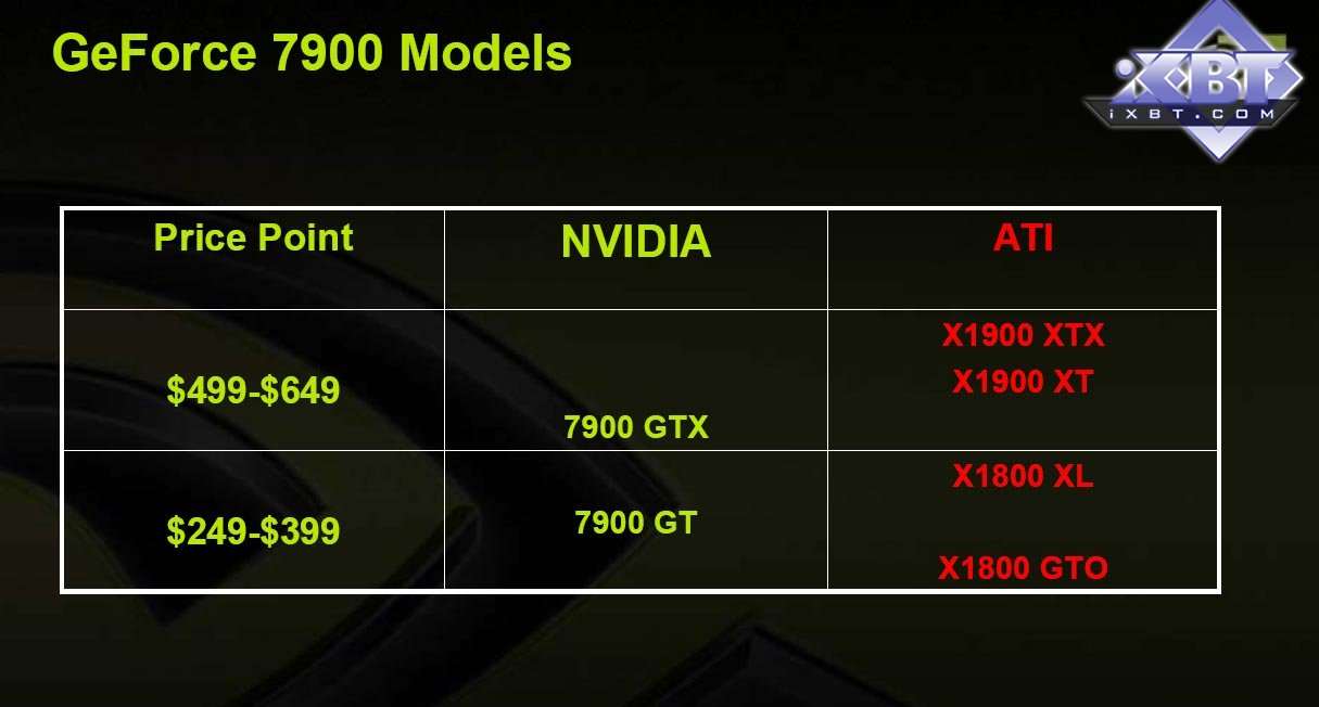
We give the floor to our colleague, Alexander Medvedev. He will describe the new products: Not much time has passed since the announcement of RADEON X1900 (R580), not so disputable a solution as R520 that doesn't even pretend for leadership, as NVIDIA decided to batter in another nail to the foggy marketing prospects of ATI in this season. Nobody doubts that ATI is technologically at the frontiers of graphics acceleration, but will it be successful in terms of commercial output and mass popularity? NVIDIA announces two new chips. The key issue is the 90nm process technology (=0.09 micron). It has stopped being ATI's prerogative. One of the chips is a top solution, even though it's called G71. It's actually positioned as a stronger solution than the G70 (GeForce 7900). Later on we'll discuss it in detail. The second solution is G73 (GeForce 7600) - a curtailed modification of the G71, which should push all its competitors in the middle end segment, especially in price/performance ratio. Let's waste no time and proceed to the specifications. GeForce 7900 (codename G71) and GeForce 7600 (G73) Series SpecificationsBefore you read this article, you had better look through the fundamental materials on DX Current,
DX Next and Longhorn
that describe various aspects of modern hardware video accelerators in general and architectural features of NVIDIA and ATI's products in particular. Information about NVIDIA's flagship architecture and the previous G70 chip can be found in the corresponding article: And now let's proceed to the specifications of the new product: Official GeForce 7900 Specifications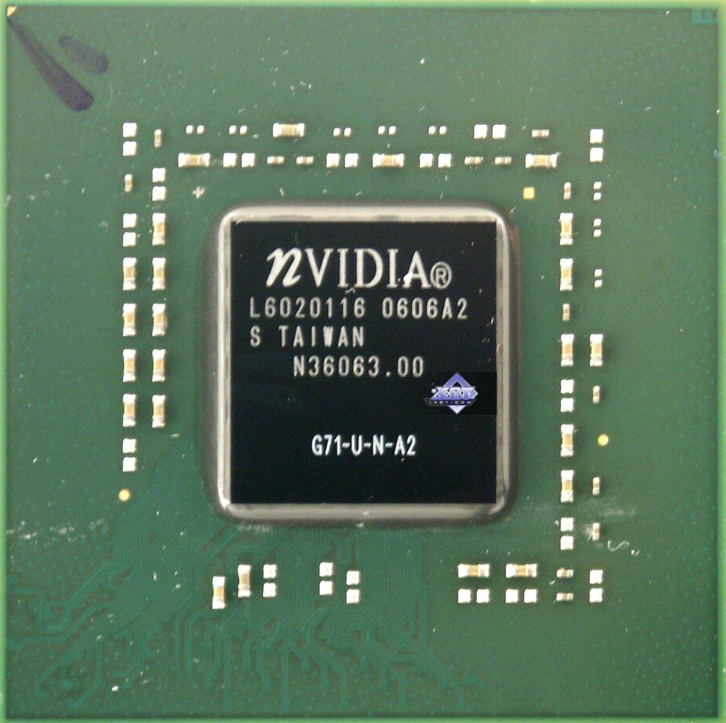
Reference card GeForce 7900 GTX specifications
Reference card GeForce 7900 GT specifications
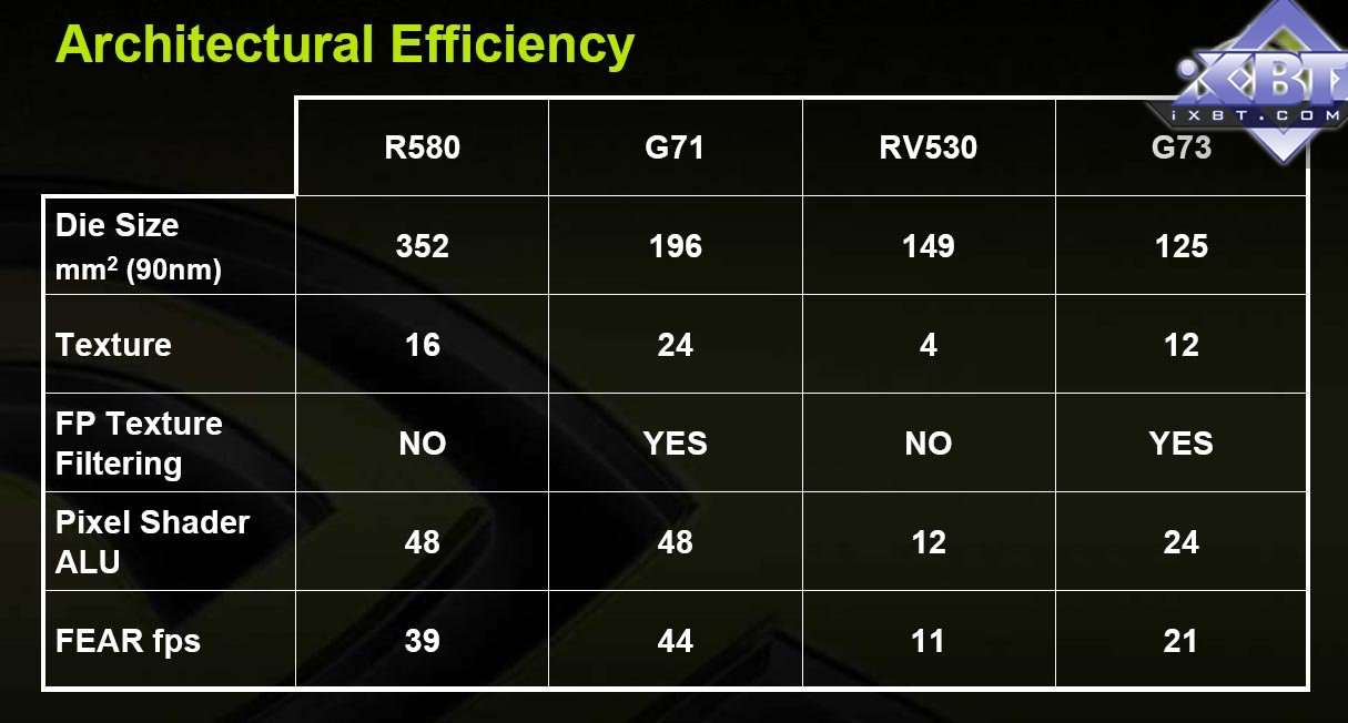
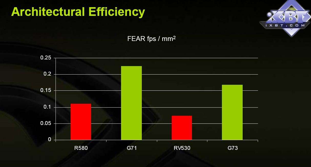
That's obviously the same architecture as in the G70. It's just manufactured by the 90nm process technology with minor modifications (in bold). Wait, minor changes - how is that? Why are there noticeably fewer transistors? Will it affect performance? Running a few steps forward I can say that it does not. Perhaps, the G70 reserved some units (for example, there were 7-8 pixel quads instead of 6, and 9-10 pixel quads instead of 8) to provide higher yield of effective chips or even for the potential Ultra modification, in case ATI had decided to launch a superior solution. To all appearances, the new G71 is equipped with units to the eyeballs - either the yield of effective 90nm chips is that good, or NVIDIA can afford more rejects (as the chip cost has dropped due to the considerably smaller surface area). Another answer to this question (considerable optimization) is also possible. But it's less likely, as it's difficult to cut down a number of transistors by 25 millions without losing performance and keeping the same architecture. But it may just be possible, let's not turn down this version from the very beginning. So, indirect reasons indicate high yield of effective chips and no manufacturing problems as well as noticeably cheaper prime costs of the new chip compared to G70. Thus, now we understand its codename (G71) - the chip is indeed simpler in terms of transistors, though it's faster thanks to the higher frequency. So, from the architectural point of view the chip offers the same features and the same number of active units. That is everything will be up to the clock frequency, which is noticeably higher, and the price, which may potentially become much lower than for the G70 due to the thinner process technology and fewer transistors. Typical power consumption of the GeForce 7800 was known below 100 Watts. And the new card is much cooler. For comparison - power consumption of the X1900 XT is about 120 Watts, which is nearly twice as high. It's noticeable in practice as well - just touch the cards (not during operation - that's dangerous, but after you turn the system off). The surface area of the chip is noticeably smaller than in the ATI competitor (R580) and the previous NVIDIA flagship (G70): 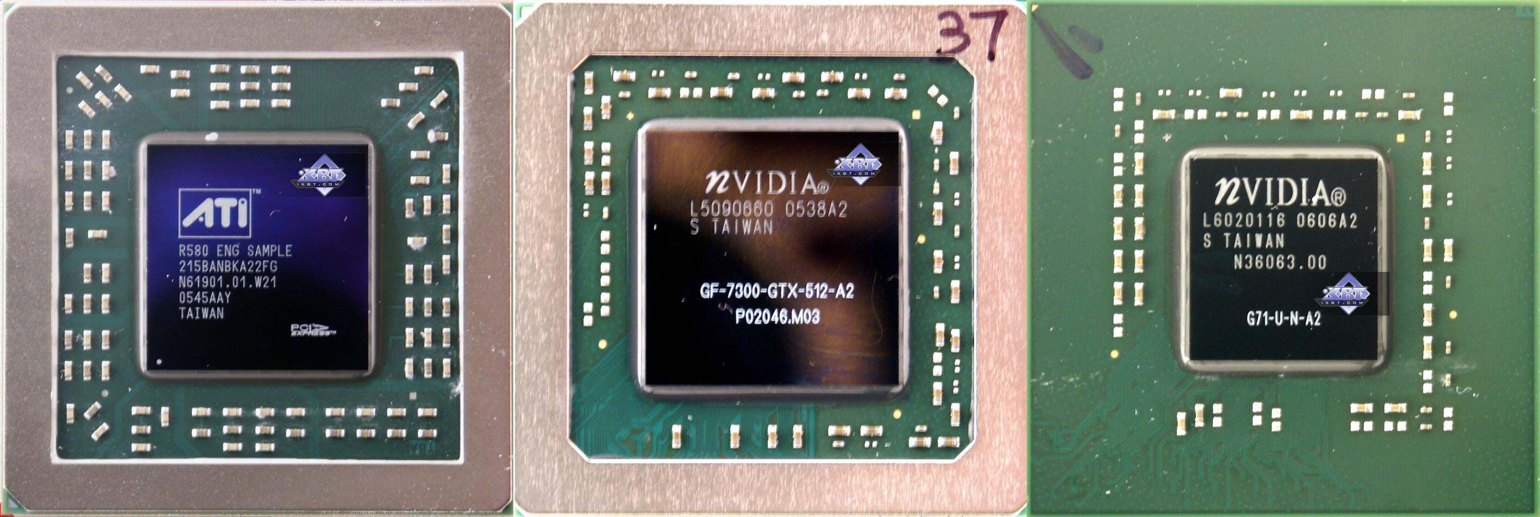 Note two integrated DualLink DVI interfaces (the time of external interface chips has gone) and the same 400 MHz RAMDAC - there is no point in higher values, analog monitors stopped developing. Another interesting innovation - Quad SLI. Astute readers may guess its function by the title. It will be discussed in detail below. The manufacturer declares hardware support for H.264 and other video compression standards of the latest generation, intended for HD, blue ray, etc. Interestingly, the NV4X also offered this support, but it's not available to NV40 and NV45 because of a bug. What concerns the new chips (NV42, 43, etc), it will also be added in the new drivers. Along with decoding, we are promised an improved deinterlacing algorithm and new post processing with enhanced clearness and improved color rendition. We'll wait and see - I wish we had more HD quality games, we've got appropriate computers but... Official GeForce 7600 Specifications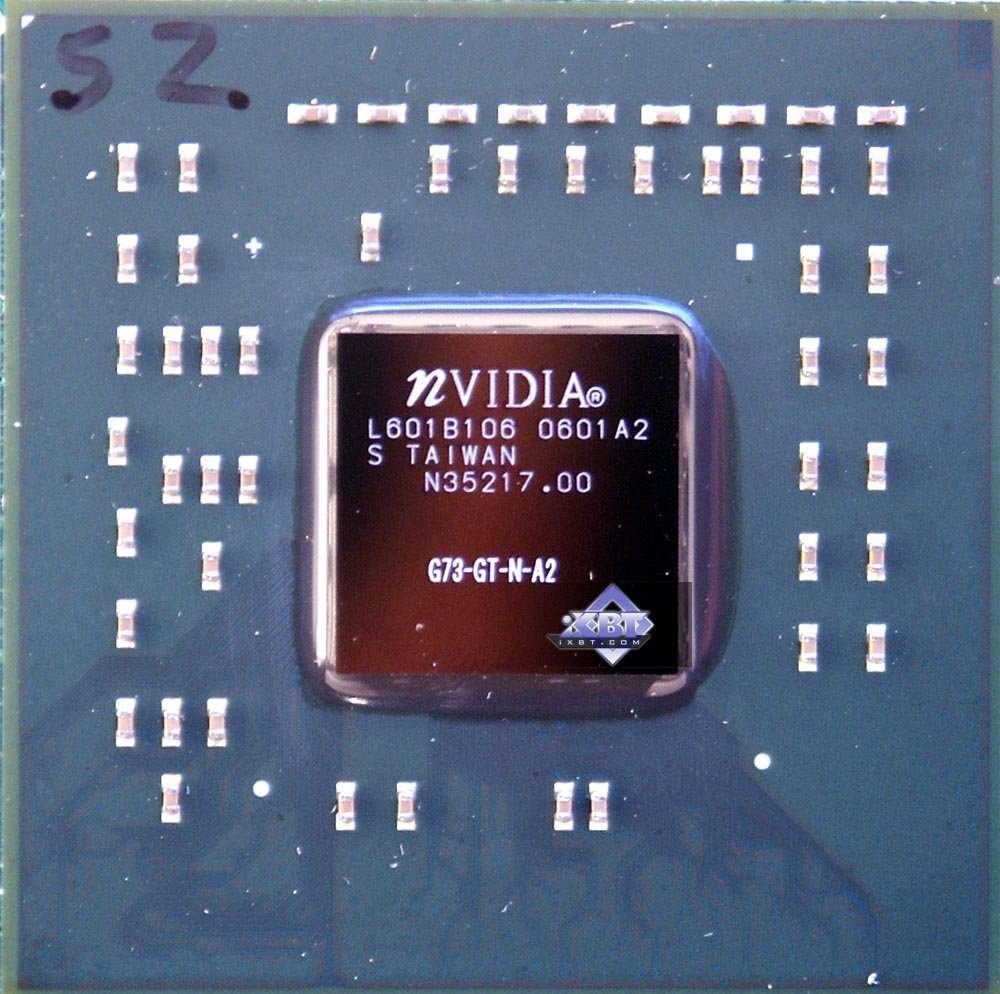
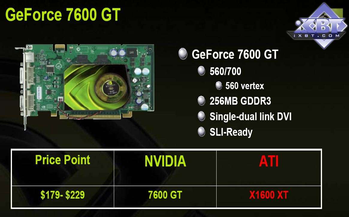
Reference card GeForce 7600 GT specifications
Differences from the G71 are highlighted with blue. So, the G73 is practically a half G71 (except for 5 vertex units instead of 4 ones). Both in terms of the memory controller as well as the pixel part. But we should make a reservation here - according to our analysis, G73 physically has 16 pixel processors instead of 12 (that is it has 4 quads). One quad is reserved for higher yield of effective chips or (you never can tell) for a solution with 16 pixel units to respond to new competitors in this sector. The chip surface area is smaller than the NV43 - but it's much faster!!! (NV43 on the left, G73 on the right) 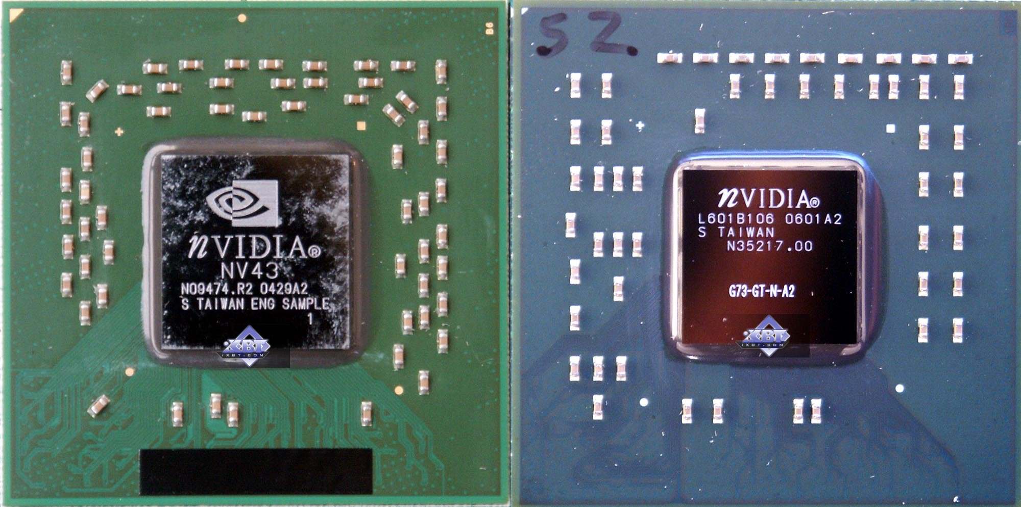 Interestingly, the codename G74 is not used yet. To all appearances, this title can be used for the inexpensive G71 reincarnation, which may also contain 20 or 16 pixel pipelines. We'll wait and see. Running a few steps forward - NVIDIA has nothing to worry about in this field. G73 with its 12 pipelines is more than sufficient. Thus, G73 looks VERY attractive, its competitiveness is beyond any doubt even here and now, after reading specifications and before any tests. Later on we'll find many practical proofs of these words. Quad SLI is an off-road for marketing fieldsSo, a new old technology - SLI for four chips. Of course, such solutions existed before, for example in industrial simulators for pilots or probably in game machines. But we have come across this technology in usual PCs for the first time. The same concerns a dual-chip GeForce card from NVIDIA that is installed into a single slot. These cards will have a special suffix - GT2. 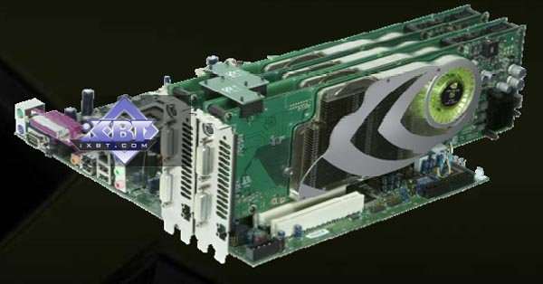 < <
It was pointless to make Quad SLI a solution for four sterling PCI-E 16x slots - such motherboards would have been too exotic and buying four identical cards is inexpedient even in case of linear performance gains. NVIDIA's solution looks more reasonable - to launch a card with two chips, which is a SLI solution in itself, and allow to install two such dual-chip cards into a SLI motherboard. Thus, NVIDIA kills two birds with one stone - it offers a SLI solution on a single card as well as allows to upgrade it to Quad SLI by installing the second card. We have no doubts that the resulting performance will be very high, may be even record-breaking. In future, we shall devote a separate article to Quad SLI and analyze its performance in various applications. As for now, we can only note that low power consumption and heat dissipation of the G71 (as well as a low prime cost, let's not forget about this factor) made it possible to launch such a dual-chip flagship. Neither G70 nor R580 would have physically allowed to design such a card complying with the modern PC specifications on power consumption and heat dissipation. The card consists of a main and a daughter cards, two-slot wide. In Quad SLI mode it's connected to the neighboring dual-chip card with two links. Thus we get a square topology - both chips of a card are connected with each other and each one is connected to another chip on the other card. 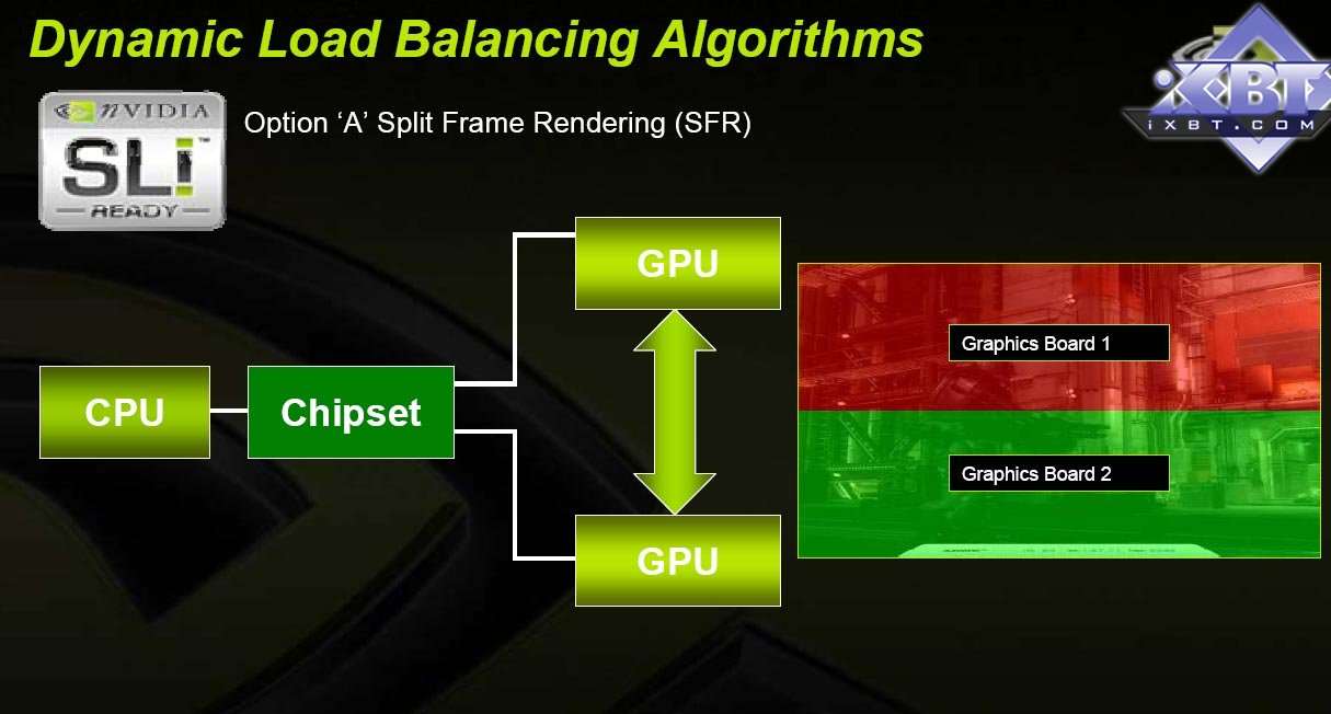 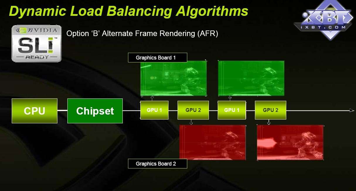 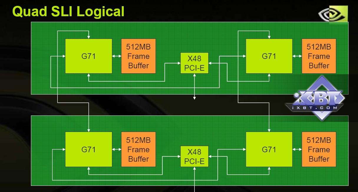
Besides, each dual-chip card is equipped with the PCI-E 16x bridge for system arbitration and access to both accelerators. It still works in the same way - there are three cooperative modes - AFR, zonal rendering (slicing a frame into four zones) and SLI-AA - using accelerators to calculate various AA samples within a single pixel. Besides, it becomes logical to combine the modes - for example 2xAFR from two two-slice frames (interleaving frames, each of which is rendered by SLI slicing) or slicing 2x SLI-AA, etc. There may be a lot of combinations, no architectural changes are required for that, SLI already contains various methods and their combinations are up to a driver. As before, a user can choose optimal settings for applications, both custom or preset. NVIDIA stresses one more time that the number of SLI applications is much higher than in case of ATI CrossFire. Unlike ATI, you don't need a special master card - all NVIDIA cards with SLI support can work together as well as all GT2 (Quad SLI) cards. Mobility issuesLow power consumption allows to use G71 in mobile devices on a large scale. Moreover, it opened the floodgates to such exotic solutions as SLI notebooks! Here is a photo of a motherboard for such notebook. You can see two accelerators, based on the mobile G71 (GeForce Go 7900): 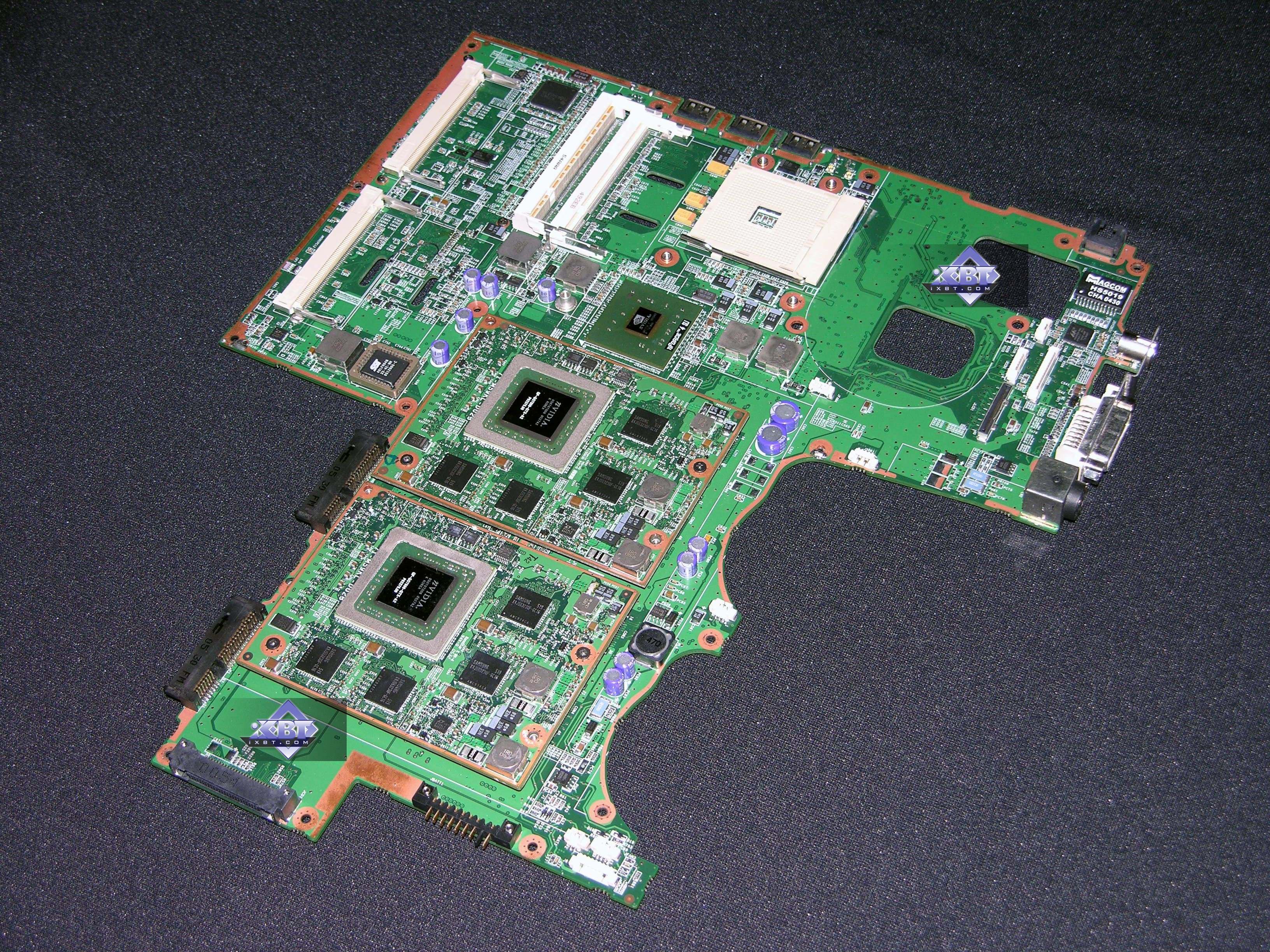
We can soon expect announcements of various solutions on G7900 Go from the leading notebook manufacturers, including SLI solutions. It goes without saying that the chip frequency will be lower than in desktop modifications, especially in a battery mode. But the core frequencies even in the smallest notebooks with such powerful video will be about 375 (GeForce Go 7900 GS) and 500 (GeForce Go 7900 GTX) MHz. It is comparable to performance of modern desktop solutions, based on GeForce 7800, that is older by just six months. The reserve for the future is obvious - no doubt, NVIDIA can launch desktop solutions offering even higher performance. ArchitectureThis part will be omitted, as there are no changes. Everything said in the GeForce 7800 review remains true. Here are several NVIDIA slides, devoted to architectural specifications of the new chips: 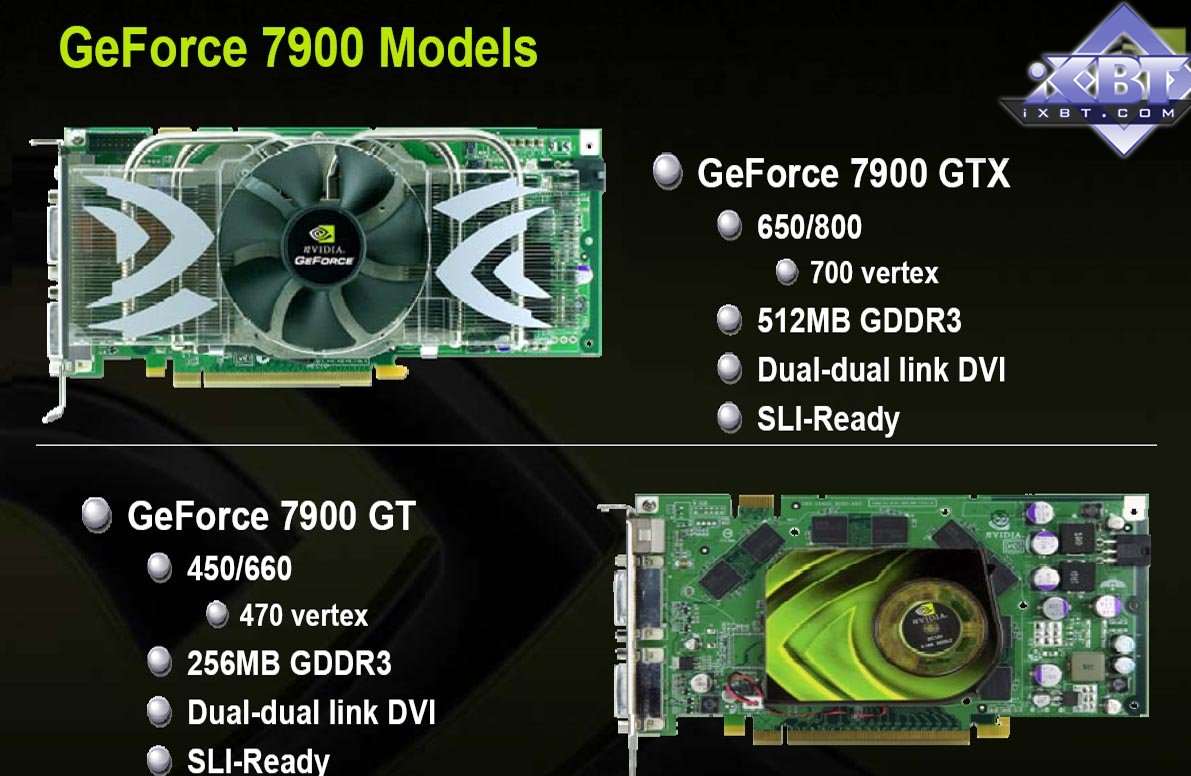

And now let's proceed to the long-awaited practical part! NVIDIA GeForce 7900 GTX/GT (G71), GeForce 7600 GT (G73). Part 2: Video cards' features and synthetic testsWrite a comment below. No registration needed!
|
Platform · Video · Multimedia · Mobile · Other || About us & Privacy policy · Twitter · Facebook Copyright © Byrds Research & Publishing, Ltd., 1997–2011. All rights reserved. |


