 |
||
|
||
| ||
|
||
|
||
| ||
For the three months after the previous article was published, there happened two major events, several minor ones, and one expected event didn't happen on the market of 3D cards. Besides, the second quarter of 2005 was marked by complete lack of any news on any manufacturers, except for the two North American competitors. As we had supposed in the previous article, S3 demonstrations were nothing more than demos. XGI plans proved to be very distant again. So, let's proceed to major events of the past months without digressing to minor things. Major events of the second quarter of 2005We'll start with ATI's events, as we did the last time. ATIFor the past months since the end of April, ATI did the following in the chronological order:
Launching Radeon X800 XL (R430) 512MBThe chronologically first minor event was the ATI's announcement of Radeon X800 XL video cards with 512 MB on board. RX800XL video cards use the comparatively new R430 chip with PCIE interface. Interestingly, the RX800XL PCB had been initially designed for 512 MB of memory, so ATI engineers had to introduce only minimal changes to the card: 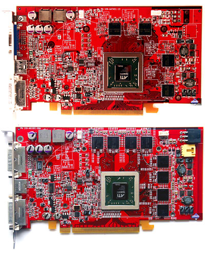 Pay attention to the additional power connector on a video card with 512 MB of memory — the increased number of GDDR3 memory chips exceeded the power consumption limit of the PCIE x16 slot. Why is this a minor event? Firstly, our tests of the Radeon X800 XL 512 MB did not reveal practically any advantage of this card over its 256MB counterparts. Secondly, the Radeon X800 XL 512 MB was not the first video card with this memory volume — so we learned nothing new in terms of influence of the additional 256MB of video memory on performance. Radeon X800 XL 512 MB cards with MSRP 449 USD occupied the top position in the line of PCIE cards based on R430:
Taking part in the announcement of MS Xbox 360 (ATI C1/R500/Xenos)Of course, this event cannot be attributed to the computer market of 3D video directly. I guess all the details on the new game console from Microsoft will be covered in a separate article. But there is one minor point that does not allow us to ignore the Xbox 360 announcement in this article. That fact is that the video chip codenamed ATI C1 (or Xenos) is actually a working prototype of a future computer chip from ATI supporting DirectX 10. What's so interesting about Xenos? Firstly, Xenos is the first video chip with unified pipelines ever created. In other words, Xenos pipelines can process pixels as well as vertices; the chip does not divide its pipelines into vertex and pixel ones. The load is distributed by a special unit that dynamically determines processing priorities: vertices or pixels. Moreover, the notion itself of the "number of pipelines" grew obsolete within the principally new Xenos architecture, because the pipelines were split into constituent parts, communicating dynamically. This chip has 16 texture samples and 48 universal ALUs (as far as we know, organized into three "cores", each of them being able to work either with pixels or with vertices, but not with both types simultaneously). As the Xenos chip specs correspond to the DX9 SM3 level at the least, the entire might of 16 sterling TMUs may be used for texture sampling in vertex shaders as well. The Xenos method to write data into a frame buffer is no less interesting: 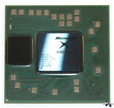 ATI divided the graphics pipe between two chips: a larger chip (232 million transistors), which processes all vertex and pixel operations (shader core); and a smaller chip (105 million transistors), mostly consisting of high-performance memory (10 MB), but also carrying the logic responsible for writing results and frame buffer operations (memory core). What's so interesting about this solution? Firstly, ROP integration into the same chip with the memory allowed ATI to connect ROP and memory with a very wide 256 GB/sec bus. In practice, MSAA comes almost "free of charge" - not only for standard frame buffer formats, but also in case of FP16 buffers for the fashionable HDR. The bus bandwidth between the shader core and the memory core is just 32 GB/sec. That is the shader core cannot take advantage of the high bandwidth inside the memory core. This very high bandwidth will actually be used only to accelerate MSAA and high precision buffer blending. What do we lose in case of such frame buffer operations? Complex post processing effects that require returning frame buffer values to the shader core, in the first place. However, we should do justice to Xenos - even in this case its post processing capacities at least equal capacities of state-of-the-art computer video cards. Such a memory architecture is not EDRAM in the traditional sense of this term (EDRAM in video cards implies memory integration into the shader core), but MS feels free to promote the Xbox 360 video system as possessing 10 MB EDRAM. ATI has an original approach to using these 10 MB of high-performance memory for rendering high-resolution frames: 10 MB are obviously not enough for rendering in HDTV resolutions, even if announced by MS. In particular, even MSAA 2x at 720p (1280x720) would exceed 10MB, in case of the standard 32-bit frame buffer with the 32-bit Z-buffer. Does it mean that Xenos cannot use MSAA in HDTV resolutions? If yes, why make this fuss with the memory core and the wonderful bandwidth of 256 GB/sec? In order to solve the problem, ATI suggested rendering in tiles. But in this case, we'd better use "in parts" to avoid confusion. Xenos renders a frame per several cycles. The first one is used to fill Z-buffer. Then a frame is processed in parts, while Z-buffer (filled during the first cycle) is used to determine which triangles belong to the currently processed part of a frame. When a processed part of the frame is completed, it's written to the Xbox 360 system memory (MSAA buffer is downsampled at this stage) and the chip starts rendering the next part of the frame. In general, the ATI Xenos architecture is doubtless revolutionary in two fields: rendering pipelines and frame buffer procedures. However, while unified pipelines are an expected development of current 3D video chips and we easily predict its appearance on the market of PC video cards in 2006, frame buffer innovations require certain software support, so they will hardly be implemented for PCs in the same way as in the Xbox 360. ATI CrossFire Announcement — the Answer to NVIDIA SLIThe first major event for the past months was the announcement of ATI's CrossFire — a long-awaited answer of the Canadian company to NVIDIA SLI, which was called either AMR or MVP even last year in December. You can read about CrossFire details in the "Asymmetric Repartee. New technology: ATI CrossFire". In this article we shall just point out the main differences between CF and SLI as well as marketing peculiarities of CF, which are becoming more prominent for the past months. So, ATI CF has three key differences from NVIDIA SLI: a different connection type between two cards for co-processing a frame, special MSAA modes, and a different co-rendering mode. Unlike SLI, CrossFire video cards are connected by a special cable, connected to DVI ports instead of special connectors on the cards (funny thing, CrossFire feels unexpectedly nostalgic in this respect for the times of 3dfx Voodoo Graphics and Voodoo 2 :-)). 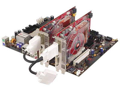 Of course, ATI tries to present this connection type as an advantage — it really is in a determinate sense — but ATI actually had no choice. The fact is that unlike NVIDIA, which initially equipped its video cards on NV45 and NV43 chips with SLI connectors, ATI sold a great number of video cards on R423, R430, and R480 chips without any additional connectors — that is they had to invent something to connect them in tandems. So ATI engineers came up with this solution: you have to buy a new card for a CF configuration, so called CrossFire Edition (these video cards are equipped with a unit that pools resources of several video cards); buy a chipset, which currently supports CrossFire; and then use your old PCIE video card based on R423, R430 or R480 chip in tandem with the new video card (it goes without saying that video chips must be the same, but they may have different clocks and number of pipelines) using an external DVI-DVI cable. These are the officially announced video cards: Radeon X800 CrossFire Edition (based on R430) and Radeon X850 CrossFire Edition (based on R480, which can safely be connected to R423 — they differ only in frequencies). At the time of the announcement, CrossFire configurations were guaranteed to operate only on ATI Radeon Xpress 200 CrossFire Edition chipsets, but this limitation has to do with thorough CrossFire tests on different platforms rather than with technical peculiarities of CF. The second major difference between CrossFire and SLI is new MSAA modes, available to CF owners. In brief, this advantage comes to using programmable MSAA sampling patterns, sagely implemented in the R300 chip already: if one card processes 4 sub-pixels and the other card processes 4 sub-pixels taken from other grid points, we'll get a pixel with 8 sub-pixels when the results are merged, i.e. we actually get MSAA 8x. However, there is no performance gain in this case, because each video card renders each next frame completely. Moreover, ATI did not stop at that and implemented two modes, where the final frame merges two frames with shifted geometric coordinates — these modes allow CF owners to get texture anti-aliasing with an alpha-test (quite useful in some cases), being sort of an answer to hybrid MSAA+SSAA modes available in GeForce cards. And finally the third major difference is the new multi-chip rendering mode, when a frame is divided into rectangles, which are processed by the cards in staggered order — that's why this technology is called CrossFire. This mode is claimed to have more efficient load distribution between the cards that process a frame. Theoretically, this mode have all the limitations as Split-Frame Rendering. It's also interesting to note that ATI thoroughly implemented SFR as well as AFR modes in its CrossFire technology — both modes are clones of the NVIDIA SLI counterparts. We've come to the sad point in our narration about ATI CrossFire: it's currently impossible to check all the points of the Canadian company and our own theoretical assumptions, because even a month and a half after the announcement, chipsets and video cards with CrossFire Edition labels are not on sale yet. Why? We shall publish our thoughts on this issue in the next chapters. Delaying the Announcement of R520-based Video CardsWe've come close to a major event in the ATI's camp: long awaited, but still to be waited for — the announcement of R520-based video cards. This announcement was initially expected in May, then it was postponed to June, then we heard the dates around the end of July, and the latest intelligence speaks of September. What has happened with R520? According to the ATI report during the last quarterly stockholders' meeting, the company has no problems with the chip architecture, the delay has to do with the insufficient yield of effective chips from the 90nm TSMC production line. That is ATI have run into the same problems with the new process technology as NVIDIA did with its NV30 chip. But it's too early to compare the utterly unsuccessful and practically unavailable NV30 chip with the R520: the R520 will hardly follow in the tracks of the NV30 in terms of insuperable gap from its competitor in performance and image quality. In our opinion, the worst of possible scenarios is approximate parity in performance and image quality between the R520 and the G70, the former being launched on the market six months after the latter. The R520 chip may just as well be more powerful than the G70, even though we are 100% sure that the number of pixel pipelines in the R520 will still be 16. But rumours and speculations will be covered in the concluding part of our article. NVIDIAWhile the majority of events in the competing camp (except for the Xbox 360 announcement) turned out small fish for various reasons, NVIDIA was steadily winning back its authority (lost two years ago) in May, June, and July, 2005.
Taking part in the Sony PlayStation 3 announcement (NVIDIA RSX)A couple of hours prior to the MS Xbox 360 announcement, there happened another purely console event, which will inevitably have an effect on the computer game market: Sony ventured to announce PlayStation 3. Last year in December NVIDIA announced its contract with Sony for PlayStation 3 video system development — it makes this company one of the key players of the entire project. So, what do we know about the NVIDIA RSX chip used in PS3? Not much officially (most details are protected by NDA and provided only to game developers for the new Sony console). We know for certain that the RSX chip will be manufactured by the 90-nm process technology on Sony's plant in Nagasaki. We know that the RSX chip will have a dedicated 128-bit bus to 256 MB of GDDR3 memory operating at 700 MHz (effective 1400 MHz). The chip uses a high-speed FlexIO bus instead of the AGP/PCIE interface, designed by Rambus with the total bandwidth of 35 GB/sec (20 Gb/sec CPU→GPU and 15 GB/sec GPU→CPU). RSX operating frequency is 550 MHz. Here the official info stops (we shall ignore the mythic figures of the peak performance on unknown operations, if you please) and rumours and conjectures start. It's up to you to decide on their correctness. Rumours have it that the RSX chip is nothing else than the G70, ported to the 90nm process technology, deprived of half of memory controllers and equipped with FlexIO interface instead of PCIEx16. Rumours have it that Sony backed and filled until the last moment in its choice of NVIDIA, so that NVIDIA had no time to overhaul the G70 PC video chip for the console market (in particular, EDRAM buffer would have been not out of place for stable back compatibility with PS2; and the 256 bit memory bus would have been surely preserved, if they had had enough time for better chip layout). Another rumour runs that initially the chip for PS3 must have been designed by Toshiba, this chip would have been called RS. But after a great deal of negative reviews from game developers for PS3 and probably after X360 specs were looked through, Sony decided to change the video system manufacturer. To sum it all up and remember everything written about Xenos, the picture becomes quite interesting: featuring higher performance, RSX offers no significant innovations in memory operations. In other words, the RSX bandwidth may be insufficient for rendering in HDTV resolutions with AA — especially if you remember that the RSX memory bus is not 128-bit. To proceed with our comparison, we cannot fail to notice that the Xenos chip is much more advanced in functional terms: while the G70 (and consequently the RSX, if the rumours are true) supports only DX9 SM3, Xenos is "nearly" a DX10 chip. There is an opportunity that the RSX will work noticeably faster than Xenos with DX9 code, but the question of insufficient bandwidth for MSAA at 1280x720 and higher still remains undetermined. Of course, any technical comparison of two gaming consoles is purely conventional: these platforms are too different to dully compare numbers of pipelines, bus bandwidths, and frequencies. But we shall still risk an assumption: while Xenos is more flexible, allows more complex effects, and easily provides antialiasing in any resolutions, RSX is a "grinding-mill" for comparatively simple shaders — but this "simplicity" must be balanced so that the chip is not idle most of the time waiting for the rendering results to be written into a frame buffer. Besides, we shall review PlayStation 3 in more detail, wait for the new articles on our web site ;-) GeForce 7800 GTX (G70) Announcement
The main event of the past three months is certainly the announcement of GeForce 7800 GTX, based on the new NVIDIA chip — G70. You can read a detailed account of new chip's features with performance tests in the article, laconically called NVIDIA GeForce 7800 GTX 256MB PCI-E. 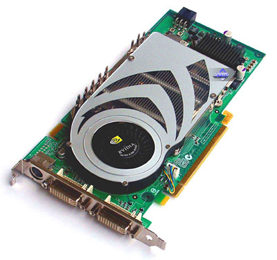 One of the nice "innovations" of the GF7800GTX announcement was availability of the new cards in stores a week after they had been announced. Compared to the birth pangs of GF6800U and RX800XTPE, you feel much gratification from the immediate availability of the currently most powerful video card. However, the reasons for such NVIDIA's success are not that obvious and even partially accidental: try to find a competitor to the GF7800GTX. What, there aren't any? That's right. The fact is that the G70 chip had been designed by NVIDIA rather long ago (some GF7800GTX cards are equipped with the chips manufactured in February), but successful sales of GF6800 cards and the lack of serious competition made NVIDIA wait for the R520-based cards. As we have already mentioned, they refuse to appear. NVIDIA had been waiting for a long time but still didn't see it come out — the side effect of this prolonged wait is the immediate availability of GF7800GTX video cards in retail. Of course, we cannot say that it has nothing to do with the time-proven 110nm process technology by TSMC, or with the streamlined NV4x architecture, but in our opinion the main reason of the GF7800GTX availability was the unexpected ATI delay, not NVIDIA's efforts.
You must have noticed that NVIDIA, after ATI, raised the upper MSRP limit up to 599 USD. But before you burst into sobbing and complaining about greedy capitalists, you should remember the first real prices for the GF6800U cards and then look at the retail GF7800GTX prices. An interesting picture we see: with the 499 USD MSRP, the GF6800U cards used to cost 600-700 USD for six months; while the GF7800GTX cards with their MSRP at 599 USD can be now found at 600-700 USD, a month after their announcement. In other words, such a price "increase" should be rather called "adjusting the recommended price to the reality". Moreover, prices in the West start from 500 USD already — 100 USD lower than the MSRP! What did the G70 chip bring besides the expected performance gain? The chip remains the same as far as the supported API functions are concerned: DX9 SM3, no MSAA for FP16 buffers, poor dynamic branching performance in pixel shaders — a complete counterpart of any NV4x. Strange as it may seem, key innovations of the G70 fall to the antialiasing quality and to the power consumption optimizations. Antialiasing innovations are covered in detail in our GF7800GTX review: this video chip is the first to offer antialiasing for transparent textures with alpha test; besides, the gamma correction option is now "legalized", users of NV4x video cards had to edit the registry to get it. However, according to NVIDIA, gamma correction is implemented on the hardware level in the G70 chip, while the NV4x-based cards use the software implementation that influences the performance. We shall check whether it's true in another article. What concerns power consumption optimizations, there is no need to write anything about it — just have a look at the photos of the video card to see that NVIDIA refused to equip it with a two-slot cooler, despite the increased clock and complexity of the die. And finally, we should remember another feature of the G70 chip, which was revealed after the GF7800GTX cards had appeared on sale: individual frequencies of various functional units of the chip. While pixel pipelines (shader ALUs and ROPs) in the GF7800GTX card operate at 430 MHz, its vertex pipelines run at 470 MHz! Besides, frequencies of pixel pipelines and ROPs change at huge 27 MHz steps, user settings are rounded down. That is if you set the G70 chip to 450 MHz, you will actually get 459 MHz (432 default + 27 = 459); but if you try to set it to 470 MHz, you will still get 459 MHz, because 459 + 27 / 2 = 473.5, that is the frequency of pixel pipelines will go up to the next step (486 MHz) only when the user setting is higher than 473.5 MHz. Operating frequency of geometry pipelines is set exactly to what you specify, but BIOS always adds 40 MHz to it. 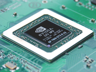 We don't know yet users' limits in controlling G70 frequencies (we have found three frequencies so far: frequencies of shader ALUs and ROPs (they are changed synchronously) as well as the frequency of vertex pipelines). According to some indirect signs, the 27 MHz step is not immutable, pixel pipelines in the G70 chip can be clocked with more precision. Moreover, perhaps all these frequencies can be controlled independently: to set different unrelated frequencies for shader ALUs, ROPs, and vertex pipelines. However, this functionality is interesting only from the theoretical point of view. For example, the option to raise ROP frequency independently would allow several interesting tests, to find out how much the G70 is limited by the performance of ROPs, which number remains the same since the NV40. NVIDIA SLI evolution — new video cards and featuresNVIDIA SLI events can be described in the following phrase - "I see the target!" :-) The CrossFire announcement provided NVIDIA with a reference point for SLI. The company immediately started correcting the flaws in comparison with the offer from the Canadian company. I guess there is no point in mentioning the SLI support in the G70 chip, announced at the end of June. But there is one thing worth mentioning: SLI configurations made up of two video cards without SLI connectors. This opportunity was first implemented in Driver 77.72 for GF6600 video cards (these drivers can also be used by any SLI cards to omit the SLI connector). Driver 77.76 added SLI support for the new GF6600LE video cards (we didn't even review these cards — they are the same GF6200 cards based on NV43 under a new name, the main and only difference is SLI support on the driver level).  It was certainly a forced move — GF6600 video cards have no SLI connectors, but NVIDIA wants very much to make the ostentatious SLI technology available even to the poorest users. Here is the question — why hasn't ATI done the same thing? Why make a fuss with complex DVI connections? There are two reasons. Firstly, SLI is noticeably less efficient without the connector than the regular SLI, as the sync traffic and rendered frames are transferred via the system PCIE bus. Secondly, old ATI chips have no CF support — unlike absolutely all NV43 chips, which dies contain a SLI unit. The next major SLI event was the SLI AA presentation — a direct answer to complex antialiasing modes, implemented in CrossFire. Ironically, SLI AA is available to all SLI owners right after the beta release of Drivers 77.76, while ATI CrossFire has not yet appeared on sale... NVIDIA borrowed the idea from ATI, but it added its own patches and adapted it for NV4x/G70 chips. Like ATI CF, the SLI AA mode demonstrates no performance gain from using SLI — both cards calculate the entire frame on their own. Due to a little shift in geometric coordinates (not less than a quarter of a pixel in SLI AA 8x and even less in SLI AA 16x) when two frames are merged, samples fall to different grid places resulting in the notorious antialiasing:  An advanced user will notice right away that SLI AA 8x is nothing less than MSAA 4x + MSAA 4x, while SLI AA 16x is 8xS + 8xS. The resulting grids in both cases are rather ugly and far from being effective due to the fixed sampling pattern in NV4x/G70 chips and impossibility to take more than 4 samples in MSAA mode. At the same time, SLI AA 16x mode is numerically superior to the maximum AA ATI CrossFire mode — MSAA 6x + MSAA 6x. When opportunity offers, we shall check which of the modes offers higher quality. But I'd like to note that the quality difference in modes higher than MSAA 4x goes down to zero, especially in dynamic games. While 8xS mode in GeForce cards still makes some sense (texture antialiasing and "side-effect" anisotropic filtering), you will have to use a magnifying glass to find differences between 6x and 4x modes in ATI cards. That's why it's hard to say whether all these crazy modes (like ATI CF 14x or NV SLI 16x) make any sense... Provoked by the CrossFire announcement, NVIDIA decided not to stop at what had been accomplished and promised that the new drivers (starting from Version 77.62) would allow SLI for the same cards from different manufacturers (the cards must have been completely identical before that — including BIOS versions); video cards would allow independent overclocking in due course; in prospect, SLI may be allowed on motherboards with PCIE x16 + PCIE x4 slots. So, ATI CrossFire announcement was definitely a success as far as NVIDIA's answer to it is concerned :-) Then, several manufacturers decided to launch dual-chip cards based on NV45, mentioned in the previous article. In particular, among these manufacturers are ASUS (ASUS Dual 6800GT, you can read about its prototype in the previous article of the series) and Gigabyte (Gigabyte 3D1-68GT): 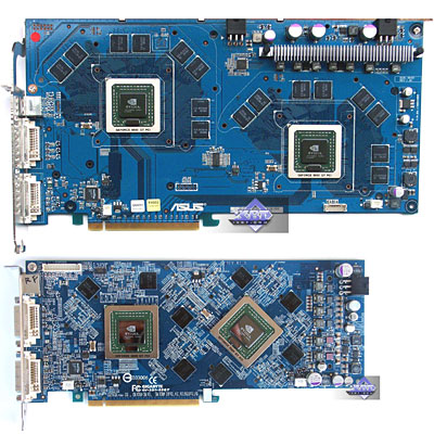 De facto, such cards are also SLI models with their own compatibility problems due to huge dimensions (Gigabyte unexpectedly stands out here with its rather sane PCB size), and SLI support peculiarities in NVIDIA drivers. But it seems to me that the manufacturers are too late: who needs these noisy voracious monsters with a lot of compatibility problems, if a single GF7800GTX card at a similar price provides the same or even higher performance level, plus offers a number of improvements in antialiasing quality? Why manufacture these cards at all? The only reasonable assumption is that these cards were designed for the G70. If that's true, we shall soon get such tandems based on the new NVIDIA chip. It's scary even to imagine the price for such monsters. Launching NV48-based video cardsThe last NVIDIA event to be mentioned in our article is the NV48-based cards sneaking into the stores, we have written much about it in the previous text and turned out to be wrong. So, NV48 is the same good old NV40, ported to the TSMC production line, either 130nm or 110nm. In other words, NVIDIA completely abandoned IBM chip manufacturing services, all new chips from NVIDIA will be manufactured by TSMC. GF6800GT PCIE has an interesting fate — if the GF6800U PCIE is replaced by the GF7800 cards and the AGP sector has NV48, will the NV48 chip be used in GF6800GT PCIE? The question still remains undetermined. Current video cardsBefore we proceed to 3D video prospects for the nearest two or three months, let's sum up all the changes in the video card lines, mentioned above, and have a look at what the leading manufacturers offer for different graphics buses. Video cards from ATI and NVIDIA, July 2005
Nearest Future of the MarketHaving cleared up the issue with the current situation on the market, let's proceed to the most interesting part — speculations on its nearest future :-) Let's start with ATI again. ATIThere is nothing much to guess about — the nearest event must be the announcement of video cards on the long-awaited R520 chip. We have more or less come to know the specifications of this chip, though we may still be mistaken:
The R520 presumably supports FP16 blending, which allows FP16 HDR without much efforts (and performance loss to additional calculations in pixel shaders), as it's been done in NV4x/G70 chips for over a year. ROPs, completely orthogonal to the frame buffer format, must be a nice addition. They will allow MSAA in case of FP16 HDR — such a function is not available in the NV4x/G70. However, the question of practical use of this antialiasing remains: G70 performance in HDR mode in Far Cry and SC: Chaos Theory discredits the idea of further performance drop — it's too low even now. The R520 will obviously support CrossFire. Moreover, there is a chance that ATI will give up an external DVI connection and will use a special bridge like in NV SLI. Moreover, we shall risk an assumption that CrossFire (motherboards and video cards of the CrossFire Edition) will not actually appear on the shelves prior to the R520 cards. The fact is that even two Radeon X850 XT PE cards offer the performance level comparable to a single GeForce 7800 GTX. That's why there is practically no point in launching them on the market — they are evidently inferior to a cheaper and more functional solution from NVIDIA. So, it all depends on the R520 announcement. When will this long-awaited event happen? There are different rumours. We can just establish the fact that July 26 is over (the planned date of the announcement of R520-based cards before GF7800GTX would appear), meaning that the announcement is again put off for later. When? It will most likely happen at the end of August or even in early September. We doubt that ATI and its partners will be able to provide R520-based cards on such a mass scale in a couple of weeks after the announcement, as it happened with NVIDIA and its G70 chip. What then? The R520 announcement must be followed by the announcements of RV515 and RV530 chips — low end modifications of the new architecture from ATI. It's too early to think about their specs, but we can safely assume that these chips will preserve all the functions of their senior brother — R520. We also have information that the RV530 will be the first ATI chip offering the double rate of writing results into Z/S buffer in case of no MSAA — similar to all NVIDIA chips, NV30 and higher. The RV515 chip will occupy the bottom position in the new series of ATI video chips, having replaced various RV3x0. Then ATI should present a new flagship — the R580 chip. It's too early to speak of the release dates: we have heard various dates, from this year in autumn (almost simultaneously with the announcement of the delayed R520) to Spring 2006. Of course, it's silly to discuss the specs, but we'll still risk a number of assumptions. The R580 chip will most likely retain the 16-pipeline architecture, but its shader ALUs will be significantly overhauled, resulting in noticeably higher efficiency of the R580 relative to the R520, when executing code with a lot of Shaders 2.0 and 3.0. The assumption about further development of the R300 architecture also looks logical (all current PC video chips from ATI have developed from the R300 chip to this or that degree; only the console Xenos falls out of this list, it really uses a new architecture). R580 will most likely be the DX9 SM3 chip as well. It's dangerous to look further into the future — R6x0 chips must comply with the base DX10 requirements and must have an architecture similar to ATI Xenos. These chips should be expected in the second half of the next year together with Windows Vista aka Longhorn ;-) NVIDIAThe nearest plans of this company include the launch of new video cards based on the familiar G70 chip — we can certainly expect GeForce 7800 GT in August. It's intended to replace the former leader GeForce 6800 Ultra (MSRP will probably be 499 USD). We already know approximate characteristics of the new product: 20 pixel pipelines, 7 vertex pipelines, and 400 MHz core. According to the preliminary tests, G70 performance in this configuration is somewhere between the GF7800GTX and the GF6800U. Besides, don't forget that NVIDIA may launch a faster video card based on G70 — both the overclocking potential of GF7800GTX video cards as well as their modest cooling system will allow that. Such GeForce 7800 "Ultra" might work at about 500 MHz. However, the necessity to launch such a card will be dictated by ATI R520 success versus the GF7800GTX. The nearest new chip from NVIDIA must be the G72, it's already mentioned in the latest beta versions of ForceWare drivers. According to our information, the G72 must stand between the G70 and the NV43, having replaced the remains of the NV45 and the NV42 chips in PCIE sector. However, reliability of this information gives rise to much doubt. Anyway, in the first six months NVIDIA will replace all NV4x chips for the new G7x ones. The chips will presumably rank in the following order: G70 > G72 > G74. Besides, NVIDIA plans on presenting the G71, information on this chip is quite controversial so far. Another important event for NVIDIA shall be the release of ForceWare 80 drivers. Besides quite possible performance optimizations in the shader recompiler for G7x chips, Drivers 80 may introduce an interesting procedure of distributing vertex shader calculations between GPUs and an idle CPU. It will come in handy for dual core CPUs, where one of the cores will be useless in games for quite a long time. To be continuedThat's where we shall end the third article of our series :-) The next review of the 3D video events on the computer market will be available on iXBT.com this Autumn. By that time ATI will hopefully produce the new R5x0 chips, NVIDIA will offer G7x generation models, and perhaps S3, Matrox, or XGI will rally from the coma...
Danil Gridasov (degust@ixbt.com) September 1, 2005. Write a comment below. No registration needed!
|
| |||||||||||||||||||||||||||||||||||||||||||||||||||||||||||||||||||||||||||||||||||||||||||||||||||||||||||||||||||||||||||
Platform · Video · Multimedia · Mobile · Other || About us & Privacy policy · Twitter · Facebook
Copyright © Byrds Research & Publishing, Ltd., 1997–2011. All rights reserved.


