 |
||
|
||
| ||
|
||
|
||
| ||
Today, on January 19, 2005, Intel has officially announced the new mobile platform codenamed "Sonoma", but it officially goes under the same "Centrino" brand. It can be considered the third generation of this platform already (the first Centrino generation is 130 nm Pentium M processor (Banias) with 852 series chipsets, the second – 90 nm Pentium M processor (Dothan) with 855 series chipsets). The most important components of the new platform are a Pentium M processor with a new Dothan core revision (which will be reviewed in this article) and a "mobile" modification of the 915 series chipsets – Intel 915GM/PM (depending on the video system: integrated or external). Testbed configuration (Acer TravelMate 8100 Notebook)
Identification
We shall start the examination of the new platform from its identification.
For this purpose we'll use the latest version of our universal tool
– RightMark Memory
Analyzer. 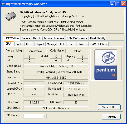 Information about the processor. The program correctly identified it as Pentium
M on Dothan core signed (Family/Model/Stepping) 06D8h, which differs
it from our previous testee –
Pentium M (Dothan) processor signed 06D6h. Actually, it's this fact
that gave rise to this review. So, we can see that the processor operates
at the frequency close to 2 GHz (taking into account that the
system was powered from line supply), FSB frequency – 133 MHz
(533 MHz Quad Pumped), multiplier values may vary from 6 (800 MHz)
to 15 (2000 MHz). But it should be noted that CPU can also operate
at 600 MHz in maximum power save mode – as it turned out,
by means of reducing FSB frequency to 100 MHz. However, that's
another story, we'll try to write this review in the nearest future.
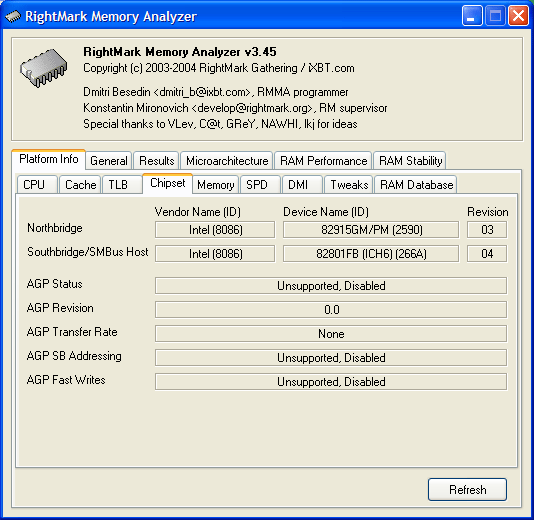
Main information on the chipset. The new i915M got the ID code of a PCI-device – 8086h:2590h. The first number denotes a manufacturer (Intel), the second – a device model. For conscience' sake we'll confess that we cheated – at first we identified PCI Device ID of the new northbridge (you can look it in for example in Device Manager OS Windows XP), and only then we added its identification into the SysInfo module of RMMA. What concerns the southbridge – it turned out the same ICH6 (8086h:266Ah device code). However, the new platform may use a newer revision of the latter (04h).
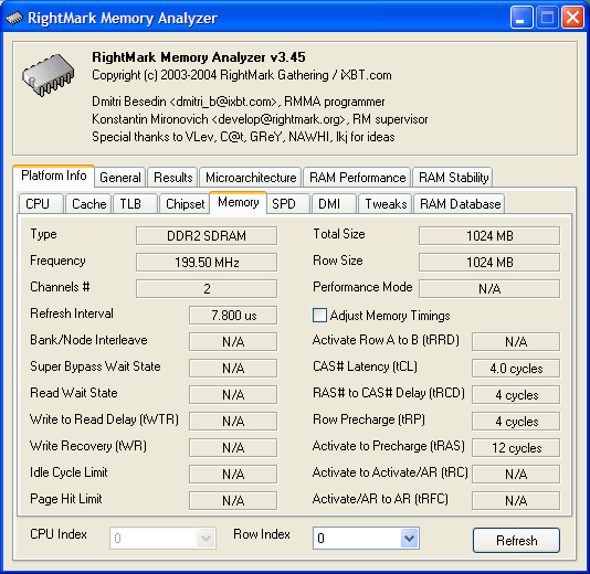
Memory settings. Memory type – DDR2, memory bus frequency – 200 MHz (DDR2-400), access mode – 128-bit (dual-channel). Thus, the peak memory bandwidth is 400x128/8 = 6.4 GB/sec, typical of modern Pentium 4 platforms. However it looks excessive for this case, because the peak throughput of the FSB is only 533x64/8 = 4.33 GB/sec. Besides it should be noted that 4-4-4-12 memory timings are typical of DDR2-533 rather than of DDR2-400. Let's proceed...
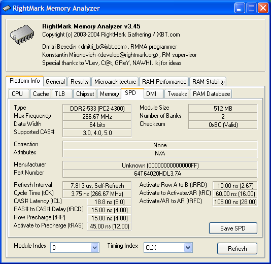
SPD data of the installed memory modules. Well, these are really DDR2-533 modules (unknown manufacturer). That's really redundant, because DDR-333 modules would do quite well (or at least DDR2-400, if DDR2 was so necessary – in fact this necessity really exists, considering lower power consumption of the latter). Well, notebook manufacturers know better which components to use in their systems. Speaking of the latter...
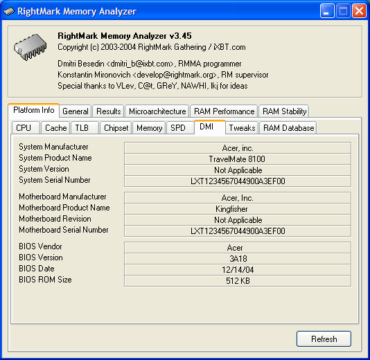 Detailed content of the DMI area in system BIOS is impressive! It contains not only the manufacturer (Acer) and notebook model (TravelMate 8100), but also the serial number of the device, information on motherboard manufacturer, as well as the version and date of BIOS. Let's wind up with identifications and proceed to the main testee – Pentium M processor with a new Dothan core revision. Our review will resemble a comparison: we'll publish test results with short comments, and if they differ from the test results for the previous model, we'll provide more details on the existing differences. CPUID data
The characteristics above have only one difference, which we have already described: the core stepping changed from 6 to 8. Brand ID and Cache/TLB characteristics remained the same. Real Bandwidth of Data Cache/Memory
Memory bandwidth versus block size curves are approximately the same in all the three cases (MMX/SSE/SSE2) and correspond (on the qualitative level) to the curves obtained for the previous Dothan revision.
 Average real throughput of Data Cache and RAM L1/L2 Data Cache capacities – 32 and 2048 MB respectively, Cache organization type – inclusive (that is L1 data is duplicated in L2). L1 Cache throughput for reading/writing (~8.0 bytes/cycle), L2 throughput for reading (4.36 bytes/cycle) and L2 throughput for writing (3.24 bytes/cycle) completely match the previous values. Only the average memory bandwidth has been changed, which is not surprising, considering the difference between DDR-333 (used in Centrino platform) and DDR2-533 (used in this platform). It's 2.6 MB/sec for reading and 830 MB/sec for writing (the latter is approximately twice as high as in the previous platform). Nevertheless, both of them obviously rank even below the theoretical limit of the FSB throughput (4.33 GB/sec), to say nothing of the maximum theoretical DDR2-533 bandwidth (8.53 GB/sec). Thereby, let's try and estimate the maximum memory bandwidth. Maximum Real Memory Bandwidth
As in all other Intel processors, the intelligent results for maximum real memory read bandwidth can be obtained only by Software Prefetch method (as well as reading/writing cache lines), while for maximum real memory write bandwidth – by the Non-Temporal Store method.
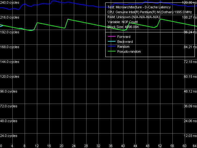
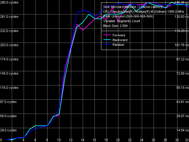
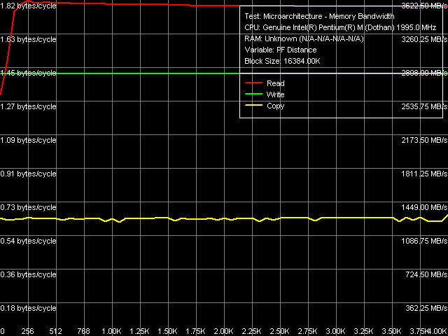 Maximum Real Memory Bandwidth, Software Prefetch/Non-Temporal Store Maximum reachable real memory bandwidth for reading is 3.62 Gb/sec, and it's still smaller for writing – just 2.83 GB/sec. Again these parameters are far from the theoretic maximum (estimated by the maximum FSB throughput – it's 83.6% and 65.3% correspondingly). Note that the overall picture of the prefetch test has slightly changed – the gain from Software Prefetch here is much higher (about 40%) than in previous tests (about 15%). Average Latency of Data Cache/Memory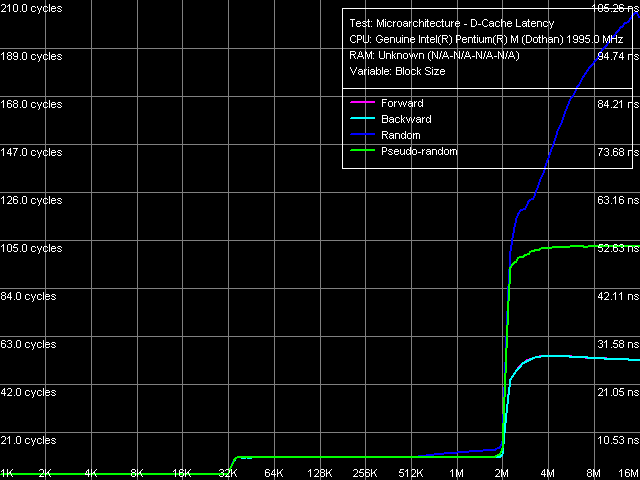 Data Cache/Memory Latency, 64 bytes stride size The overall latency picture (on the qualitative level) remains practically unchanged – one should only note a strange smooth dip of latency curves for forward and backward access at the increase of the necessary memory block (within 4-6 MB).
Quantitative latency ratings are given in the table below.
Note the considerable drop in memory access latency (4 MB block), which can be the result of improved Hardware Prefetch logics of the processor or the result of using a new i915PM chipset instead of i855PM. At the same time, latencies in reading integer data from L1/L2 Cache of the processor remained at 3 and 10 cycles correspondingly. Minimum Latency of Data Cache/Memory
As usual, in order to measure this value, we'll use the method of unloading BIU by inserting "empty" operations between memory access operations. Besides, unlike the previous test, we'll use two methods – with the stride size equal to the effective line size of L1 Cache (64 bytes) and of L2 Cache (128 bytes), which will allow to estimate the influence level of hardware prefetch (effective only in the first case) on the test results.
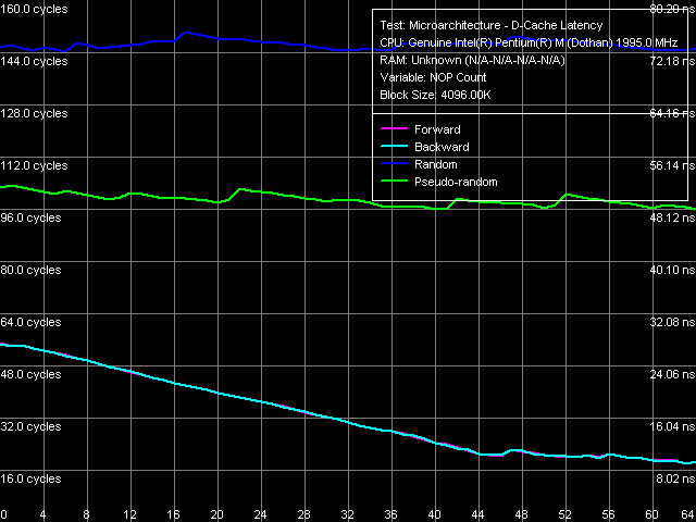 Minimum memory latency, 64 byte stride size
The first case: minimum latency of forward/backward walk reaches 9.2 ns (12.0 ns for the previous model), pseudo random – 48.2 ns (versus 57.0 ns), random – 72.5 ns (versus 87.8 ns). Thus, the new platform demonstrates reduced latencies for memory access with Hardware Prefetch in all cases.
 Minimum memory latency, 128 byte stride size And now let's evaluate more "correct" results (from the point of view of measuring latency of memory as such instead of memory system on the whole). In cases of forward, backward, and pseudo random walks we got the same (it means that Hardware Prefetch is not working) minimum value of 95.8 ns – higher than the worst result (random walk) in the first case. Minimum latency of random access is still higher – 112.7 ns. As we have already repeated several times, this is connected with depleting D-TLB resources when walking a comparatively large memory block. Data Cache Associativity L1/L2 data cache associativity The general picture of data cache associativity is obvious and needs no explanations. L1 data cache associativity is equal to four (not eight, as specified in CPUID descriptors), L2 associativity – eight (that is it matches the official value). We saw the same picture in the previous revision of Dothan core. L1-L2 Cache Bus Real Bandwidth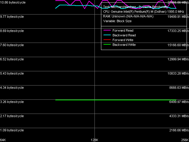 L1-L2 Cache Bus Real Bandwidth
L1-L2 Cache Bus Real Read Bandwidth falls within 10.78-10.86 bytes/cycle (which is insignificantly higher compared to the previous core revision), write bandwidth of this bus remained unchanged and is equal to 3.24 bytes/cycle.
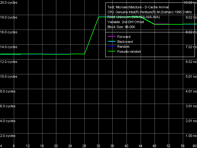 Data arrival test on L1-L2 Cache bus The results obtained, as well as results of the data arrival test (see the picture above) indicate the 128-bit bus organization, which is proudly called "Advanced Transfer Cache" (i.e. the same title as in Pentium 4 processors, claiming the 256-bit organization). You can read about the basis of the 128-bit L1-L2 cache bus in Pentium M processors in our previous analysis. Hardware Prefetch: Additional detailsIn our previous platform analyses we have never described the L2 D-Cache Line Size Determination test results, considering it something obvious and requiring no explanations. Nevertheless, this test can reveal some additional details on the hardware prefetch algorithm, implemented in all modern processors (in order to "hide" latencies when requesting data from memory). This test proved especially useful for the relatively recent implementation of the two methods for measuring memory system latency on platforms with Pentium 4 processors.
Let's provide a brief overview of this idea. It's a modification of the "data arrival test", which measures dependence of the overall latency in reading two closely spaced elements on the distance between these elements. It uses a relatively large "main" stride size – 512 bytes, which allows to vary the distance between elements in a wide range, from 4 to 508 bytes inclusive. And if the second requested element is located in the same cache line as the first one, the overall latency remains more or less constant. But if the second element falls in the next cache line relative to the first element, the total latency spirals up, because loading two elements from two different memory lines into L2 Cache requires much more time compared to loading two elements from the same line. Thus, the inflection point will give us the size of the cache line. That's how the ideal case looks like:
 Determining L1 Cache line size But that's only an ideal case (though it's a result of real measurements, only with a relatively small block size fitting into the L2 cache – that is L1 Cache line measurement). However, this may also occur in real cases, when determining the L2 Cache line size – for example, in AMD K7/K8 series processors. In our case (Pentium M) it looks much more complicated. 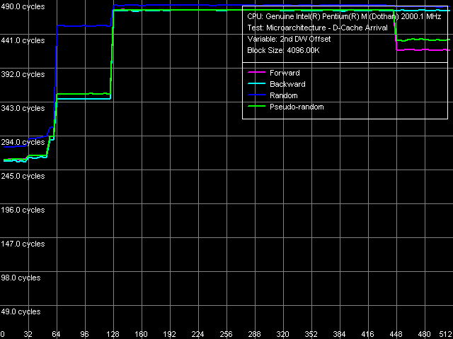 Determining L2 Cache line size, Pentium M Dothan (Stepping 6) 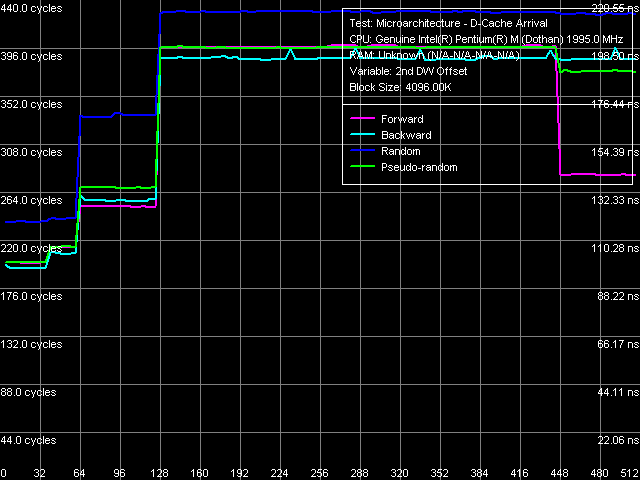 Determining L2 Cache line size, Pentium M Dothan (Stepping 8) Moreover, you can easily see in the pictures that Hardware Prefetch differs in two different revisions of the Dothan core! (pay attention to the forward walk of the 448-512 byte area). The difference found can well explain some of the differences demonstrated earlier – the lower latency of the memory system on the new platform in particular. I-Cache, Decode Efficiency
You can see the test results of decoding/executing simplest independent instructions compared to the previous results in the table below.
The results obtained look identical at first sight. However, considering the high measuring precision and good reproducibility of the test results, we have to admit that the new revision of the Dothan core is worse at executing instructions. In absolute values this is especially noticeable in decoding/executing "large" instructions like 6-byte CMP (#3-6). Which suggests an idea about a possible increase of the pipeline length at least by one stage... "I-Cache Latency"That's quite an abstract notion, that appeared in the latest RMMA versions, 3.1 and higher. It means the execution time of a certain number (depending on the block size) of unconditional jump instructions, spaced at a given distance (stride size) from each other. 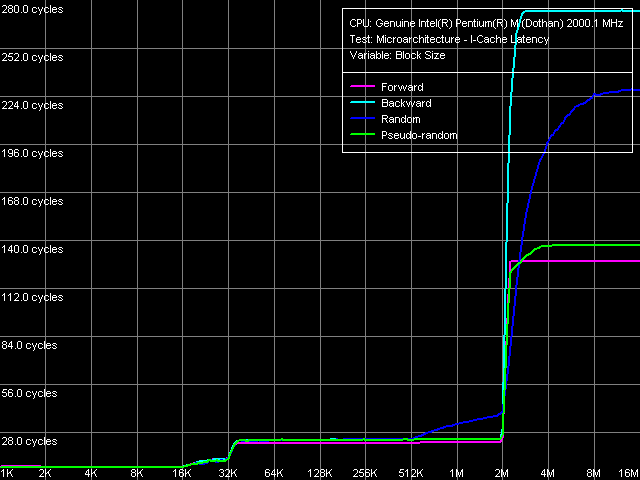 I-Cache Latency, Pentium M Dothan (Stepping 6) 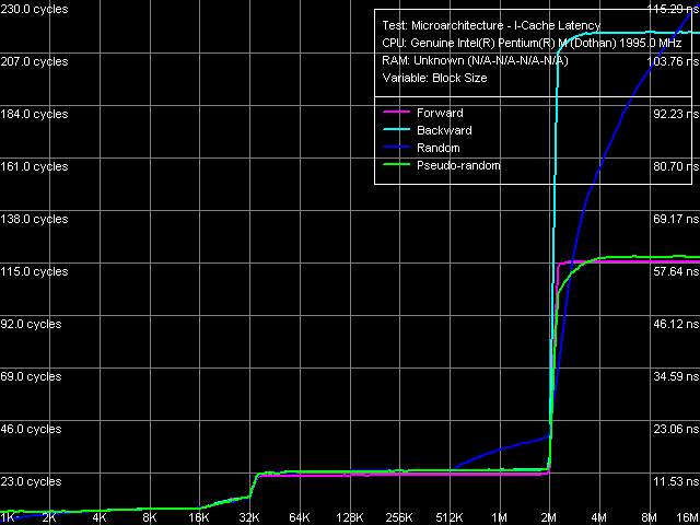 I-Cache Latency, Pentium M Dothan (Stepping 8) The curves, obtained at two different steppings of the Dothan core, reveal another interesting issue: aside from the reduction of the total latency in executing code from RAM (from 280 to 230 cycles), the new revision also has a modified ratio of random and backward sequential access curves for this area. The new core revision executes the code in backward order more effectively compared to random order, while the old revision does it vice versa. Though, you shouldn't forget that code execution in random order, to say nothing of the backward order, is a rare perversion :). Nevertheless, its analysis again allows to reveal the differences between Hardware Prefetch in different revisions of the Dothan core. I-Cache Associativity
Aside from latency, we can also estimate associativity of L1 I-Cache as well as the common L2 Code/Data Cache.
 I-Cache Associativity In this test we got distinctive curves that indicate the 4-way associativity of L1 I-Cache, and the 8-way associativity of L2 Cache. The very same results were obtained for the early Dothan model (data cache associativity and code cache associativity). TLB Characteristics
Let's determine the size and associativity of the D-TLB Cache.
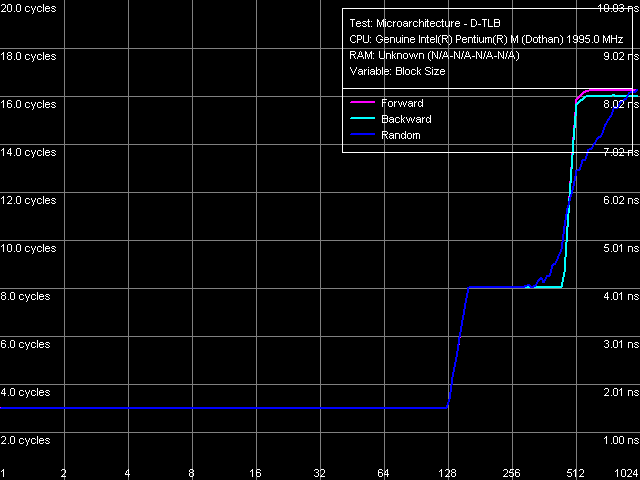 D-TLB size
The standard picture: D-TLB size is 128 entries, buffer miss penalty is 5 cycles. The inflection at 512 entries is connected with L1 Cache overrun (512 x 64 bytes = 32 KB).
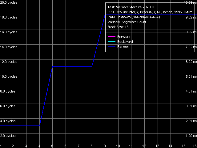 D-TLB associativity The picture of D-TLB associativity is much more interesting. It is characterized by two leaps (which is much more typical of two-level TLB, each level having a different associativity). The first leap corresponds to the true 4-way D-TLB associativity, the reason for the second leap, seemingly corresponding to the doubled associativity, is totally incomprehensible... Especially if you take into account that the early Dothan model didn't have it. Thus, D-TLB in the new core revision has been obviously changed, but it's impossible to understand what changes and why.
Let's proceed to I-TLB Cache.
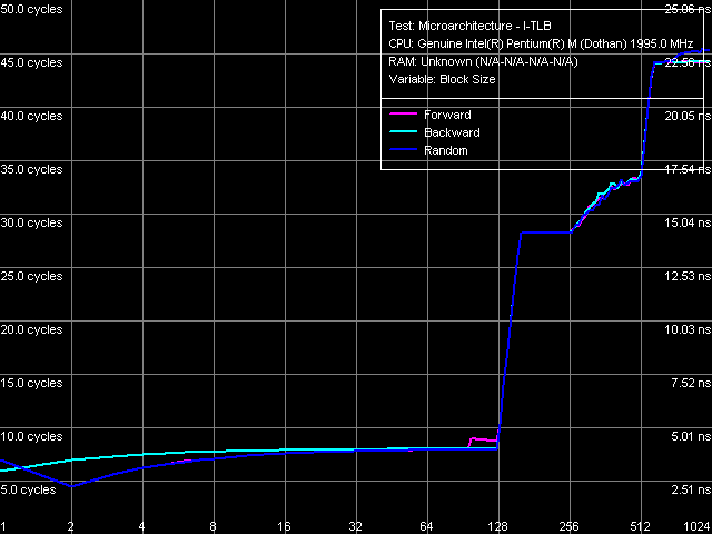 I-TLB size
The result of measuring the I-TLB size perfectly matches what has been obtained previously. Its size is 128 entries, buffer miss penalty is approximately 20 cycles.
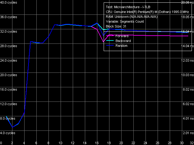 I-TLB associativity I-TLB associativity picture is quite clear and it corresponds to the one obtained for the early core revision (I-TLB associativity is equal to four). Thus, unlike D-TLB, I-TLB suffered no changes in the new revision of the core. Conclusion
That's about all we can presently say about the latest revision of the Dothan core in Pentium M processors, a key component of the new Sonoma platform. It certainly has some changes on the level of core micro-architecture, most of them are obviously beneficial. For example, the improved Hardware Prefetch algorithm, which has become a tad closer to its excellent NetBurst counterpart, implemented in Prescott core. Nevertheless, the work in this direction can be carried on in order to reach almost 100% efficiency of the BIU implementation, which has been already reached in the Prescott core. And what concerns our today's testee and the new platform on the whole – we just have to see how this new platform will approve itself in "high-level" tests, that is in real applications.
Write a comment below. No registration needed!
|
| |||||||||||||||||||||||||||||||||||||||||||||||||||||||||||||||||||||||||||||||
Platform · Video · Multimedia · Mobile · Other || About us & Privacy policy · Twitter · Facebook
Copyright © Byrds Research & Publishing, Ltd., 1997–2011. All rights reserved.


