 |
||
|
||
| ||
|
||
|
||
| ||
IntroductionAn attentive reader has both pros and cons. On one hand, he/she usually gets the idea of the article. On the other hand, sometimes such readers guess what the author didn't mean to unveil. A technical presentation is not a less odd thing. One one hand, they are anxious to tell you as much as possible about their product. But if everything is uncovered, then what to speak of at launch? Besides, in this case the competitors will get a chance to adjust their plans. That is why a poor marketer looks for a balance trying both to eat a fish and not to get his ears wet :). As you know, AMD keeps on promising to release new-generation processors based on the Hammer core - Athlon 64 and Opteron. The first is meant for the desktop market, while the other for the server sector. Now we will look into and analyze information we have about these processors. As you remember, the new AMD's processor have several key elements:
Now let's dive into the peculiarities of all the parts. Here are they: Opteron and Athlon 64:   An unexpected problem with the Opteron processors was revealed by the engineers of the service center. They asked a very simple question: where to put the warranty stickers? :-) x86-64 architectureThe x86 didn't have key changes for a long time except attaching new instructions which were used for the first time by Intel in the Pentium MMX. Key features of instructions addressing, memory segmentation, x86 instructions themselves didn't change since the i386 - that was the last revolutionary processor. And today a challenging step was made by AMD which brings us into a new epoch of changes. It's the first time since i386 when the x86 architecture is extended, not just supplemented but really extended. The matter is not that now everyone can have a 64bit computer. An ordinary user doesn't need it badly (maybe only in cryptography as it gets the best gain with 64bit calculations; a bit later we will show the figures). The matter is that the x86 architecture (new) has leeway for developing. Besides, this architecture handles some flaws of the x86, for example, it uses a flat memory in the 64bit mode, the number of general-purpose registers is extended up to 16 (later on you will see the benefits). That is why first of all, let's look through the list of users who need 64 addressing and 64-bit calculations today:
Those who don't need these new features may not use them - nothing changes for 32bit applications. Besides, you can use 32bit applications in the 64bit OS. This technology isn't going to be expensive, according to AMD, - it increases the number of transistors by 2%-3%. It's mainly connected with TLB extension (Translation Lookaside Buffer; it is used for accelerated page conversion), as well as with extension of all kinds of buffers and all pipelines and data paths up to 64 bits. Maybe the estimation for transitors given by AMD is true (especially because there is a cache with a lot of them), but the die's area must be greater than they declare. Anyway, the x86 architecture dominates regarding the installed systems and existing software. Over ten years already the x86 is said to live its last days (though it managed to live longer than many RISC processors) and was predicted to be replaced with a new architecture. Of course, IA64. However, AMD proved that the x86 architecture does have some potential to develop retaining its very important advantage - the installed data base. I doubt that even the most ardent optimists would welcome the idea of spending fortunes for the new IA64-based equipment and software. That is why this evolutionary approach must be admitted to be sparing for end-users. Moreover, such approach allows using this solution in several market segments which is definitely much more beneficial... I'm not going to go into details of the x86-64 architecture because:
Now let's dwell on the processor modes. Apart from the standard modes known yet since the i386 there is only one added - Long mode. When it's enabled (LME =1), there are two submodes: compatibility and true 64bit. When you use a 32bit OS it makes no sense to use the 64bit mode. But when you move to the 64bit one, you can use either the old 32bit software (then you choose the compatibility mode) or new 64bit one. Moreover, it takes much less time to switch between the submodes of the Long mode than between the processor modes. In the table below you can see the processor modes available for a programmer: 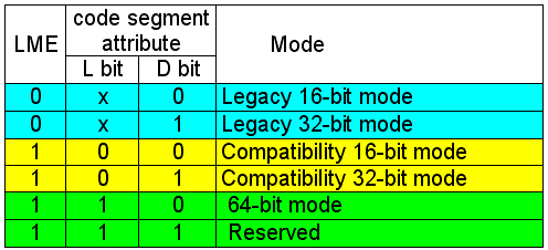 The symbol "x" means that when LME is set to 0, the value of the L bit is ignored. As you can see, the processors support 64bit, 32bit and 16bit modes - this provides compatibility, isn't it? I don't know what Reserved might mean. One of the reviewers says that maybe in this case the processor turns into DSP. It's a mad idea, but if AMD realized it, this processor would be second to none in some kinds of operations. :-) However, it can be much more trivial - maybe this combination is not needed today, and it's just left for future. To make possible to use advantages of the x86-64 architecture, 8 additional general-purpose registers, 8 additional SSE2 registers and other software tasty things it's necessary to have a compiler. Without it one would hardly feel a desire to develop programs for this processor manually... If it turns out to be inconvenient, AMD will have financial problems as well. AMD realizes it, and at present they develop several independent versions of the compiler together with famous software development companies. I won't unveil their names - AMD will do it if necessary. You just should know that at launch the processor will have the required support of the compiler allowing using its architectural advantages. Release of the processor without a compiler is also possible - the processor perfectly executes the old 32bit code. But, still, it's much better to put the processor into production paired it with a proper compiler. To demonstrate full compatibility of its baby AMD tested the new processor in over 50 OSes. Here are some of the configurations:
Now let's move to the processor itself, in particular, to its core. Processor coreFirst of all let's focus on the changes in the core and look at its block diagram: 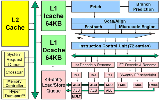 The I-cache (instruction cache) is of the same size as in the Athlon - 64KB. It's also a dual-channel partially associative solution. The block size is 64 bytes. There are two sets of tags - fetch port and snoop. The content is protected with parity check. The D-cache, data cache, is also dual-channel partially associative. In the current modification it supports 40-bit physical and 48-bit linear address, though this parameter can be increased if necessary. The data block is also 64 bytes. The added feature is MOESI protocol of operation of the L1 cache earlier used in the AMD760MP(X) chipset. It supports two 64-bit read/write operations each clock into different banks! There are three sets of tags - port A, port B, snoop. The fetch latency of this cache is 3 clocks in case of aligned addressing, and 1 clock if it is not aligned. By the way, it's quite low penalty, - in the Pentium 4 the figures are 6 to 10 clocks for unaligned data, according to different test techniques. Intel doesn't say a word about it. Hardware prefetch is supported. All data are ECC protected. As for the TLB, some sources say the TLB have capacity of 40 inputs, others mention 32.... But both stress that the L1 TLB are entirely associative and support both 4K and 2M/4M pages. It must be very good news for those who like calculations - large pages are often used in scientific calculations. But it's unknown whether the TLB is of the same size both for standard 4K and 4M pages. I could find information only in one source saying that 4K pages go with 32 inputs, and 2M/4M with 8 inputs. Contrary to the TLB for L1 cache, the L2 TLB supports only 4K pages, but the capacity is 512 inputs with 4-channel associativity. I also saw an indication at a page catalog cache of 24 inputs - it's unclear what effect it makes. I must say, there are different levels of the same TLB for L1 and L2 caches, rather than different TLB. Besides, AMD assumes that the TCB has twice greater capacity compared with the Athlon XP, while the delays are smaller (!). Usually, it's vice versa... Maybe, the TLB works at a frequency different from that of the core? The simplest assumption is a double frequency. But it's only an assumption. The L2 cache is exclusive relative to the L1. It uses a 16channel partially associative organization - AMD considered it useless to increase this parameter further. Besides, it uses the pseudo-LRU scheme which reduces twice the number of LRU bits. It's not good but this parameter is not very influential. But it makes possible to speed up processing of these bits that takes place before decoding. :-) Besides, the L2 cache contains predecoded instructions (probably, the instructions and data are stuck together in advance) and branch prediction bits. It results in a unique mechanism that increases the processor's performance. Note that the decoding (or rather preparation) starts right in the L2 cache. It means that when data are moved from the I-cache, the information goes to the L2 cache which contains the reserved space. ECC bits are used repeatedly for quick cleanup/ joint use of the cache pages - it sounds vague and frightful :-). What does AMD mean? Does it use the same bits for additional information which were used for ECC information? I doubt as it could bring about no data protection... The L2 to L1 data transfer rate is increased twice (compared with the Athlon XP) - it must boost the perofrmance in many operations. But how? by extending the bus or reducing the access delays? Most likely, it's the bus extension because we need at least 128 bits in the 64bit mode for simultaneous delivery of an instruction and an operand. Or it became possible to conduct two simultaneous operations of data transfer, for example, writing and reading, which is equivalent to an increase of the effective bus bandwidth. Besides, the L2 cache supports delayed requests - 8 delayed requests for data and 2 for instructions. As usual, several buffers are supported: a victim buffer for 8 inputs, snoop buffer of the same size and a write buffer for 4 inputs. But the most important question about the L2 cache concerns its size. If it's known that the Opteron will have 1 MB L2 cache, the size of the Athlon 64's cache is a mystery. I think there will be two versions 256 KB and 1 MB because:
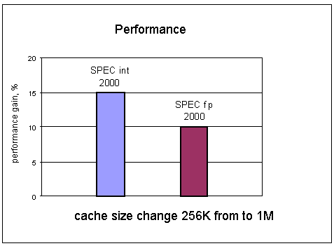 That is why I think it would be rational to develop a desktop Athlon 64 with 256 KB L2 cache and an Opteron with 1MB L2 cache. But it's rumored that a usual Athlon 64 will go with its modification for dualprocessor stations with 512 KB L2 cache. Well, the Opteron is really two expensive for such system, and the Athlon 64 doesn't work in the dualprocessor combination. That is why it sounds logical to have a modification of the Athlon 64 (let's call it Athlon DP) just for dualprocessor combinations. But as far as I know AMD will have just a desktop version with 256 KB and a server version with 1 MB of the L2 cache. The Opteron might come in different modifications, if it's needed. Moreover, the Opteron is said to have two types: one for dualprocessor configuration and the other for 4- and 8-processor systems. Both modifications will have three Hyper Transport buses each and 1 MB L2 cache. Because of the different processor architectures, it's getting more and more difficult to compare them. The Pentium 4 and Hammer have different algorithms of operation with the L2 cache, that is why it's impossible to say what is better - 512 KB of the cache of one or 256 KB of the other. The branch prediction block was redesigned. Now, for higher precision, it tracks the history of 16K transitions (it's 4 times more than of the Athlon XP) and keeps in memory 2K of destination addresses. Together with the 12-input address return stack, it lets AMD claim prediction more precise by 5%-10% in comparison with the previous generation of the processors. It gets more important as the longer pipeline (12 stages instead of 10) the processor became more sensitive to the incorrect branch predictions, but due to the lower memory access delay, the performance drop will probably be less noticeable compared to the Athlon XP. Besides, now the software prefetch doesn't turn off as the buffer takes data in, and the hardware one works better when coupled with the software one. Let's return to our data. After that they get into that part of the decoder which was redesigned most of all. The pipeline's extension is on account of the decoder as two additional stages appeared exactly there. The decoder turns nonregular x86 instructions (of the variable length) into µOPs (microoperations) of the fixed length. At one clock each decoder can process an instruction of 16 bytes (!) long and send µOPs to the scheduler which then are packed in groups of three. Here it is: 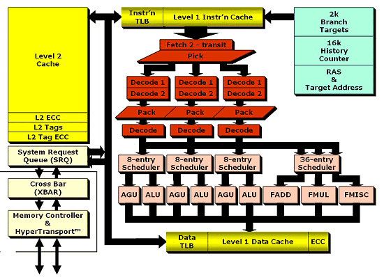 The instructions can be turned into µOPs with two different methods. The first method uses the Fastpath block to turn an x86 instruction onto 1 or 2 µOPs which (packed into blocks of three µOPs) then proceed to the scheduler. In the second case, with the Microcode decoder x86 instructions turn into a sequence of more than two µOPs (for complex operations), ready sequences being loaded from ROM (or rather from MIS - Microcode Instruction Sequencer, it's a kind of ROM that contains previously programmed sequences of microops). In comparison with the Athlon XP, there are more x86 instructions which use the faster Fastpath decoder which has smaller delays in clocks - 2 against 5. Besides, such design of the decoder brings about the following:
But note that it's not the performance that became worse but the technique of division of x86 instructions into µOps made the overall number of µOPs, the program turns into, smaller. Now we understand why AMD focused on the decoder - it's possible to have more work done per clock. But one can also think about making the overall work less. Let's go further. Data proceed to the execution devices. They are three in all: 3 integer units, 3 address generation and load units, 3 superscalar FPU - the same set as the Athlon XP has. The integer pipelines contain 12 stages (Athlon XP has 10), FPU has 17 (Athlon XP has the same). Now let's take a look at the integer units:
Here are the same data in a table:
All operations can be started every clock except 64bit multiplication (every second clock). And what about the new 64bit pipeline multiplier - is it included into the same 2%-3% additional transistors? Or there is a shift scheme similar to the one used in the ALU Pentium 4? The FPU is an entirely pipelined unit with out-of-order instruction execution, 36-input buffer/scheduler which is also able to execute some (?!) DSP instructions per clock. Unfortunately, I have found no particulars. The instructions supported are x87, MMX, 3DNow!, SSE and SSE2. In the 64bit mode both the FPU and ALU support 16 registers. What for? One of the bottlenecks for further performance increase is that the x86 architecture can have only 8 general-purpose registers. There is often a shortage of the registers for many algorithms, and they have to spend time and resources to get through. I don't mean physical registers - since the P6 register renaming is used. Many algorithms are too complicated because of the lack of architectural 8 general-purpose registers in the x86. AMD suggested alleviating the problem by adding 8 additional registers. But taking into account that compatibility with the previous software is obligatory for a general-purpose processor, it's impossible to use them in a standard x86 one. It's necessary to make a transition to the x86-64. Let me illustrate it: 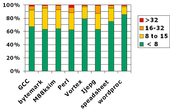 It shows the percentage of functions and algorithms in typical applications which use one or another number of registers. In the Word over 80% functions use 8 registers - the rest have to resort to register renaming and remember intermediate data. 16 registers will be satisfactory for 96% of the Word's integrated functions. The execution rate will be higher as well because it won't be necessary to use heavy algorithmic means to save registers. For the ByteMark which use a wide range of various algorithms the gain will be greater. I think scientific calculations will have the best benefit as their algorithms are very resource-demanding. What performance should we expect from the FPU? Theoretically, in x87 or SSE2 modes we can fulfill one multiplication and one addition per clock (1 Mul + 1 Add). Actually, AMD managed to achieve nearly 1.9 FLOPs per clock (peak performance in the SSE2 scalar). It's excellent! In SSE and 3DNow! modes the theoretical performance is 2 multiplications and 2 additions per clock (but of lower precision). The actual performance is 3.4 FLOPs per clock. In the tests they used not the latest revision of the Hammer core - probably the scores could be higher. The same recommendations about ALU - usage of preliminary aligned data and of prefetch which has several types: prefetchnta, prefetcht0, prefetcht1:
Besides, AMD introduces a new write method called Streaming Store, or non-temporal write. There is a special Write buffer used when placing data into the memory, neither L1 cache nor L2 cache are used. Moreover, it's not necessary to align data according to the cache's length to reach the maximum speed. As the cache is not enabled, its effective size increases, and the effective memory write speed grows up nearly twice (!). Some data make me think that there are two Fastpath units and only one Microcode unit. Well, such situation is quite possible - if the most operation go through the Fastpath, it's justified. But it's just an assumption. Memory controllerThis unit is one of the key elements that determines the performance. As you know, any type of memory has several characteristics - data bus bandwidth, sync frequency (or interconnected throughput), and delays in operation. What do we have? The Athlon 64 differs from the Opteron in several aspects - firstly, the Opteron has a dual-channel memory controller, 128 bits instead of 64 bits, more Hyper Transport buses, Socket 940 instead of Socket 754 of the Athlon 64 (the consequence of the first two items) and different cache sizes. The memory bandwidth is characterized in its frequency of operation (memory type) and the data bus bandwidth - so, it supports DDR PC2100 and PC2700 (the PC1600 is also supported, but it's not very interesting). The throughput of this memory is 2.1GB/s and 2.7GB/s (4.2GB/s and 5.4GB/s in case of the dual-channel Opteron controller). There is also a half-official support of the DDR400 standard: on one hand, it's not a problem to add it (it doesn't need changing the processor, only the controller); on the other hand, the JEDEC committee hasn't accepted it yet. That is why let's wait for the end product to clarify the situation. Recently Intel unveiled its plans about using the DDR400 (or PC3200)
in its future chipsets, that is why this standard is again much spoken
about. But, according to AMD, the memory controller works at the processor's
frequency, but the memory itself can't run at it. There are two possible
wayouts: either to make a part of the chip working at the memory's speed
irrespective of the other part of the processor (it actually means asynchronism),
or resort to divisors, and the memory's speed will depend on the core's
clock speed. I think AMD will go with the second option. Here is what I
have found:
Look at the figures in bold type - probably because of some architectural limitations the divisor controlling the memory speed can be only a whole number. That is why not all processor's frequencies will be equivalent - at certain frequencies the memory's speed will be lower than the rated one. The most obvious hypothesis is that this limitation is connected with operation of the X-bar switch that links the memory controller and other parts of the processor. It's logical that the X-bar can address the memory controller only once in a whole number of processor clocks... I couldn't find any facts that could prove this theory, but it explains well such peculiarity. The memory frequency is not a trivial thing at all. Let's draw a diagram: 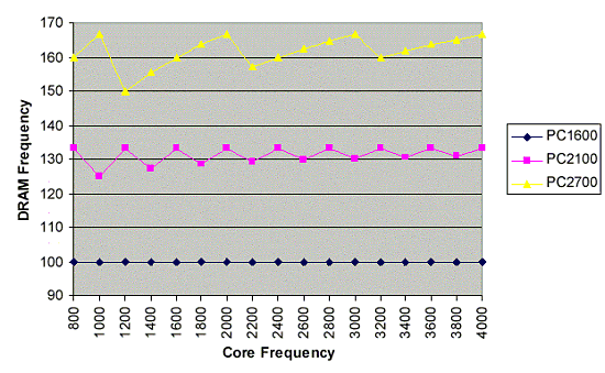 Dependence of the memory speed on the core frequency First of all, the PC1600 memory speed doesn't depend on the processor's frequency because the latter is always divisible by 200MHz, and each processor's frequency has a whole divisor. I just don't understand one thing - is the divisor only a whole number or it's also divisible by 2? The first thing is better for efficiency, but much more complicated in circuitry than a divisor divisible by 2. The PC2100 memory's frequency makes small relaxation oscillations near the rated frequency of 133 (266) MHz. The PC2700 memory's frequency acts the same way. That is why at low CPU frequencies (in case of low divisors) the memory's speed changes a lot, and as the core frequency grows up (and at some core frequencies from the very beginning) the memory's frequency is closer or equal to the rated one. Secondly, if this divisor is not fixed, overclockers will get a powerful tool - now it will be possible to overclock the memory changing this divisor, with the other components working in the rated mode. If the devisor is whole and even, the DDR400 support will require nontrivial measures - at higher core's speeds the memory's frequency will change a lot - from rated 200MHz to 133MHz (at low processor frequencies). And only at 4 - 5 Hz the deviations won't be noticeable. Or we can increase the frequency up to 200MHz - then we will be able to get the highest performance. That is why AMD plays safe with the DDR400 standard... But if the divisor is not divisible by 2, the DDR400 will always run at the highest speed... Well, to all appearances, this parameter is not ought to be divisible by 2. By the way, it's easy to explain why they choose 200MHz as the reference frequency: by the specs the Hyper Transport bus always starts at 200MHz, an only after that another frequency can be chosen. So, if we already have 200MHz, why not to use it as the reference one for the processor? I'm anxious to know what memory speed can be achieved in this system.
We found some data (probably, referring to the Athlon 64 based system
as the Opteron should have shown higher scores) demonstrated on the
system coupled with the PC2100 memory:
The scores of the Pentium 4 based system + Rambus are in blue (unknown frequency). In some cases the dependence of the memory speed on the frequency is quite strange (for example, Copy32 - 64bit), probably, because the measurements are taken at a relatively low processor speed, and effects connected with the memory frequency divisor work at their full potential. However, this explanation is not satisfactory. Another peculiarity is well seen in the table - there are some figures for the Pentium 4 + RDRAM. It's very possible that this is a system based on the i850, but not on the i850E. Even if it's PC800 RDRAM, it's impossible to overestimate the situation - such device of the memory subsystem allowed to outpace in stream operations the memory which has a theoretical throughput greater by 1.5. What will be on the PC2700? DDR400? The third quirk is also noticeable - the throughput of the PC2100 is sufficient for the processor clocked at 1200MHz - 1400MHz. At a higher frequency the memory's throughput doesn't change. Saturation of the PC2700 memory must be near 1800 MHz-2000 MHz (however, this estimation can be incorrect). Unfortunately, I couldn't find such data for the PC2700... As for memory delays, they unfortunately increase as the frequency grows up because the timing characteristics of the memory cells haven't changed. For example, AMD uses in its calculations PC2100 Cas 2, but PC2700 Cas 2.5 memory. Here are the diagrams for both types: 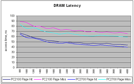 These data are obtained with the preliminary processor revision (here a processor type is not important, the Athlon 64 and the Opteron have identical controller speeds) - they can change in the final version. Besides, the data adequacy is not proved, that is why let's consider them just an estimation. The absolute memory delays - in nanoseconds - decrease as the memory and core frequencies grow up. At the limit the delays tend to the cell access time. Of course, this time also depends on whether the memory "page" is open or not, whether the address is arbitrary etc. The diagram shows that it makes around 40 ns for both memory types. I also assume that the difference between the delays at 800 MHz and 4000 MHz is on account of the memory controller (or rather, of operation of this controller and the X-bar). It's interesting that the time of operation of the controller is about 25 ns at 800 MHz (according to another source - 40 ns). But it means that the controller may not work at the core's frequency - its clock speed can be lower (but not less than 40 MHz). So, this dependence of the memory on the divisor is one more gem for overclockers. In the first core revisions the controller most likely works at the
core's speed - but AMD can get back to the idea to use the divisor
for fast speed growth. We also have some figures regarding the delays.
Are they good or bad? Look at the diagrams of the PC2100. For example,
for the core's frequency around 1500 MHz the delays are approximately 55
ns. Let's compare them with the delays for the chipsets of the standard
architecture:
The VIA KT266A chipset can boast of its decent timing characteristics. The relatively low figures of the AMD760MP(X) are caused by the ECC Registered DDR memory which has greater delays in operation compared with the Unbuffered - but even with the usual memory its predecessor, AMD760, performs at the same level. Reportedly, operation of the memory controller takes 32 processor clocks. Plus the cell access time - hence the dependence of the memory performance on the CPU's frequency. There is one more interesting figure - 180 ns for the local memory for the SUN systems. Now we can see the the delays for the Athlon 64 and Opteron are excellent! And they are going to become even better at a higher processor speed. Well, by integrating the controller into the processor (hence the low access delays) AMD made the work simpler in all situations connected with random memory access - well, to be more precise, it's not the cell access delays that will decrease (they depend on only the memory characteristics and system topology), but the overall memory reaction time. Random access to various cells happens quite often, for example, in data bases. Here the difference between the traditional chipsets and the AMD's solution will be much greater! However, it's interesting what these figures can turn into when the
system gets a load. And in a multiprocessor system. Here is what we managed
to find:
It certainly refers to the Opteron processor as the other do not support 4-processor configurations. At the start the delays are noticeable (though they are still much lower compared to other SMP systems), but they become much smaller at the higher CPU speed. However, earlier I thought that the delays depend primarily on interprocessor connections, i.e. Hyper Transport technology. Probably, its delays are not great and get lost when compared with the memory's and controller's delays. The time losses for transfer of one request to the memory of another processor via the Hyper Transport bus are estimated as 12-20 ns depending on the CPUs' speeds. But this assessment can be incorrect. I think that under the load these figures will grow up, but I can't say to what extent. But remember that the delays are just nothing compared to other multiprocessor architectures. It means that the transition of the memory controller into the processor will tell mainly upon the SMP market. I assume that AMD aims not a desktop market but primarily the dualprocessor and especially 4-processor sector. It can be proved by the careful explanation of the system's design and lack of particulars about performance of multiprocessor systems. I consider this idea logical also because the desktop market has the Barton with its L2 cache 512 KÁ and 333 MHz FSB bus to offer (probably, the bus will reach 400 MHz). It could be wasteful not to use all its potential. Besides, you should wait a lot from the desktop version, Athlon 64. Its core will be supplemented with the characteristics the current Athlon XP needs badly. It will also get the SSE2 and x86-64. But the surprises are prepared by AMD primarily for the SMP market. But let's come back to the delays. I think that the value of the delays explains why AMD chose such architecture - it managed to solve the problem of a comparatively uniform memory access (AMD calls its multiprocessor system SUMO). The delay values increase with a greater number of processors in the system because there is service information transferred providing coherence of the caches in the memory and because the data patches are longer. Besides, AMD brought in some architectural tricks into operation with the memory. Reportedly, the memory controller supports up to 16 open memory pages instead of 4 (which is the maximum for usual chipsets). Actually, I don't entirely understand what AMD means. Probably, they use the fact that the DDR SDRAM chip can keep up to 8 memory pages open. If the marketers multiplied the memory channels (two) by 8 - hence 16 open pages. The rumor has it that there is a special sensor that monitors how long every page stays open, and the sensor is able to learn, though its depth of history is unknown - in such cases a typical depth is 24 requests. The memory controller is connected with a 64bit bus working at the CPU frequency with the X-bar (and the latter with the processor's core) - at 2 GHz it results in 16 GB/sec. Now they can add any memory type - there is no bottlenecks between the memory controller and the processor. Such throughput system is superfluous for any existent memory type - but it seems that it was simpler to develop it than to think out a special bus between the X-bar and the controller. The memory controller has some other functional blocks apart from just operation with memory. For example, some users ask how an AGP video adapter will work with the memory if the memory controller is now in the processor. Now, beside the memory controller (which was integrated into the chipset) it has an AGP 3.0 tunnel AMD8151 (or other similar), Hyper Transport controller and X-bar on its way to the memory. Won't it make the video performance lower? It's also rumored that some chipset makers are developing their own memory controller for video for eliminate this problem. Now, the answer is it won't cause it. AMD integrated the Graphics Address Remapping Table (GART) into the controller. Now there is an additional data transfer stage with the Hyper Transport between the memory and video adapter - but the most difficult work of memory address renaming and request location will be carried out at a much higher speed. As a result, the speed will go up rather than fall down. The memory controller also contains a part of the PCI-to-PCI bridge. That is why almost total control over the data transfer is on the shoulders of the X-bar, an internal processor switch, thus allowing the core fulfill more intellectual work. I wish we knew more about it. It looks like an analogy of the DMA, but on a new level. And it reminds the I2O architecture. However, the good old DMA is still supported. Moreover, such design releases the processor from data transfer much better. I think that such construction must boost the input/output performance, which will have a positive effect on the overall operation. But it's my own opinion - AMD mentions it nowhere. Hyper Transport ControllerThe Hyper Transport controller is a very important component of the system as it contains a lot of innovations which were not used before in the x86 architecture. Although the nForce and nForce 2 chipsets use the Hyper Transport as well, it is only its junior version which uses almost no specific features; in fact, it works as if it were a very fast PCI. Now it's time for the Hyper Transport to show its might. Here are some interesting information about latency in operation of the input/output subsystem and how it depends on a load: 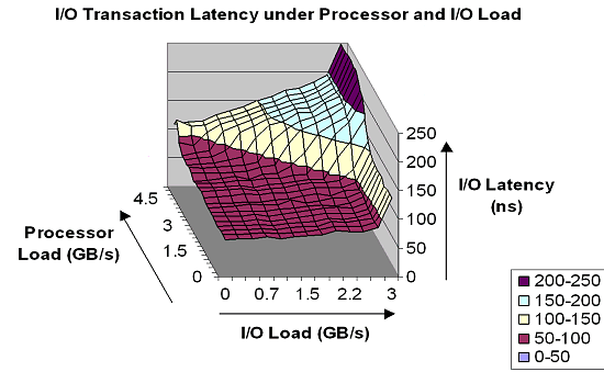 Only in case of the maximum load both on the processor and I/O system the latency increases. But 250 nanoseconds look much only in comparison with 50 nanoseconds. If we compare it with traditional I/O systems, for example, for SUN even in case of the Fire Plane (this is the upper version of the bus of 9.6 GB/s!) it takes around 100 ns only for delivery. The net value exceeds the characteristic time of the Hyper Transport. Besides, the character of dependence makes me think that such a sharp rise is on account of the CPU internal switch - X-bar, and not the Hyper Transport. Probably, this switch becomes a weak part at the greater loads. At the higher CPU's frequency the X-bar will perform better, and the graph must become flatter at all the values. It also explains why AMD keeps on promising higher scores at higher frequencies. Well, the practice will show whether this thought is true. Earlier I mentioned the latency of 12-20 ns. Here the figures are quite different. The matter is that the Hyper Transport can work in two modes: coherent and non-coherent. The coherent mode is used for interprocessor connections, while the other for I/O. Below is a diagram which will help me demonstrate a scalability level of the Hyper Transport bus: 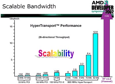 The range of speeds supported by the Hyper Transport is impressive. All in all, this bus is a very strong solution, - it combines a simple layout, excellent speeds, low latencies and good scalability; at the same time, it is compatible with the software PCI model, which is important for bringing it into the industry. Let me also show how simpler the layout of the Hyper Transport is in comparison with the traditional buses: Just compare the areas taken by the AGP 8x bus of 2 GB/s and by the Hyper Transport bus that pumps data at 6.4 GB/s. Also, let's compare it with another promising solution - PCI Express, earlier known as 3GIO.
This diagram shows the read speed: 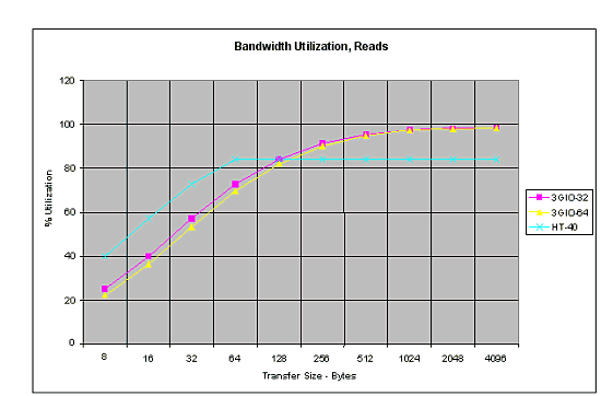 and write speed: 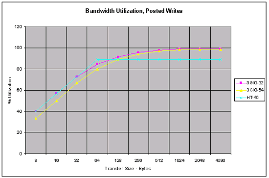 Up to 64 bytes (packet size) the Hyper Transport goes on a par or even outperforms the PCI Express, and only at a greater packet size it is less efficient - it utilizes up to 90% of the bandwidth in case of lazy write, and about 85% in case of reading. It's not bad for the buses which were created in quite different times. What does the next version of the Hyper Transport will show us? As you already know, the Hyper Transport bus supports two modes - coherent and non-coherent. The first one is used to minimize the delays, the other for the maximum performance and minimal processor load. Now it's time to proceed to another component of the Athlon 64 and Opteron systems. In closing I must say that such an architecture of the I/O system is a key for high performance of exactly SMP systems. ChipsetA chipset, as the processor's closest part, creates an impression on system's performance and reveals its pros and cons. That is why it's very interesting to see what chipset will be used for the Athlon 64 and Opteron systems. I must say AMD managed to find a nonstandard approach here. When the Hyper Transport bus was just announced, it was logical to assume that sooner or later this bus would be used in new systems based on their next processor. But the AMD's solution is not just an ordinary chipset. A classical chipset consists of two (sometimes one or three) chips one of which that contains a memory controller, AGP, and an additional bus (PCI or any other) between the chips of the chipset is called Northbridge. All possible I/O controllers including a PCI bus controller are integrated into the Southbridge. Note again that Northbridge and Southbridge are connected with a bus. It can be PCI, like in ALi's chipsets or VIA's old chipsets; it can be PCI64, like in some Server Works chipsets or AMD760MP(X), it can be proprietary buses like in the SiS, Intel or new VIA chipsets. In the end, it can be the Hyper Transport, like in the NVIDIA's chipsets. Guess what AMD has chosen? :-) Sure, Hyper Transport. Firstly, because it's their bus. Secondly, it has the highest speed for today among other available buses. Thirdly, because its unsophisticated layout allows creating inexpensive mainboards. That is why the reasons of the choice are clear. But AMD went further, much further. What do we have left out of the chipset's functions? The memory controller is in the processor, AGP is partially there as well, at least the GART. The Hyper Transport bus controller is also there. There are a part of AGP, I/O controllers and a PCI controller left. One may integrate all the remaining parts into one chip (the NVIDIA's approach) but AMD has found another way. They created three chips (under the AMD8000 series):  AMD8151, Hyper Transport - AGP tunnel  AMD8131, Hyper Transport - PCI-X controller  AMD8111, Hyper Transport - I/O controller, PCI bus controller, BIOS, and all remaining functions, that is, IDE controller, USB 2.0, network etc. Why three chips instead of one? The matter is that far not everybody needs all capabilities of the chipset. Usually, a part of them is not used, but the user has to pay, and everyone got used to this fact. Does everyone need, for example, a PCI-X bus controller which is never used at home but tremendously increases the total price? At the same time, they can't remove it at all as it's used in servers. And what about AGP and servers? An AGP video card is installed there as the transition to the AGP bus was very successful, it made PCI video cards disappear. Now you don't have to pay for the functions you don't need - there is only one chip needed to build the system - AMD8111. Of course, one can't imagine a modern computer without an AGP connector, but there are a lot of tasks where integrated video fits perfectly and dimensions are critical. Home, gaming computers should be built on the tandem of AMD8151 + AMD8111 - there is all but only necessary things. A server can go with the AMD8131 (or several ones if needed!) + AMD8111. Below you will see the schemes where these ideas are realized. Note that instead of one chipset for mainstream products, one for workstations, one or several for servers there is one set of three components which can be combined any way you want. This idea will help AMD simplify development of the technical support. Because one product (though of three components) is far not the same as a dozen of various chipsets. Let me rest a little on chipsets from other manufacturers. The CrushK8 from NVIDIA was already mentioned before - this is the first solution on one chip. It will have a pair with integrated video which will be interesting for, for example, office computers. Taking into account a high performance level of the integrated video adapter in the NVIDIA's chipsets, you can rely on good playability. Here is a slide that gives a clear idea on the oncoming chipsets from other manufacturers:  However, many board makers have already demonstrated their products based on some chipsets. The market of chipsets for the Hammer family promises to become prosperous - the processors are not announced yet but there are 8 (!) chipsets released apart from the AMD8000. Besides, AMD will probably follow its strategy it used for the chipsets for the Athlon MP - AMD has already left the market of desktop chipsets. The AMD's chipset works in the dualprocessor systems. I'm almost sure that the AMD8000 will be a reference chipset for launching the Hammer family and later it will switch to the SMP sector where the responsibility is much higher. As far as I know, there are no more chipset makers craving for this market - Server Works makes chipsets for Intel based systems, and certainly Intel is not going to make chipsets for processors of its rival. :) Athlon 64 based SystemsI have dug up some information (though it's not confirmed yet) on the row of the Athlon 64 processors. The processor will be launched at the end of Q1 / beginning of Q2, i.e. in March / April 2003. It will start at the rating of 3100+ which corresponds to the actual frequency of 1.8 GHz. Later on the line will look like this: 2800+ (1.6 GHz), 3100+ (1.8 GHz), 3400+ (2.2 GHz), 3700+ (2.4GHz), 4000+ (2.6 GHz) è 4300+ (2.8 GHz). The two latter will be released in a little while, and the former four processors already have everything prepared for the launch. Now they have to set up the mass production, which is not a simple thing to do. All the specs - both electrical and thermal - are known for these processors. It means that AMD has at least operable samples in silicon. At present, the company keeps on using the rating; AMD says that rating is not the best choice, and they are working on the measurement technique now. Later I will tell you about what they already have. The Hammer core will be manufactured at Fab 30 in Dresden according to the 0.13 micron process using the SOI (silicon-on-insulator). Multiprocessor systems. Opteron.On the one hand, regarding the memory allocation this is a typical NUMA architecture (with nonuniform memory access), because the access time will depend on whether the memory is local or not, and if not - then what processor it belongs to. On the other hand, AMD insists that it's just SMP from the software standpoint - and nothing more. There is even a name - SUMO. What do all these terms mean? First of all, let's see how these two software models differ for a programmer. To make the program run effectively, it's necessary to monitor its allocation in the memory in case of the NUMA architecture, and it's needless for the SMP one. It's because memory access times for different hierarchies in the NUMA architecture differ markedly - a wrong allocation in the memory can cause a significant performance drop. If the memory access time doesn't differ much for different processors, then it will be a software SMP model. It's much simpler, and almost all software for SMP x86 architectures is developed exactly for such software model. These are only the main differences, there are some more minor ones. Now, when the criteria are formulated, we have to get some data on access times in the SMP Opteron systems... Do you remember the diagrams of memory latency above? There were figures for 2 hops... Here is a hop: 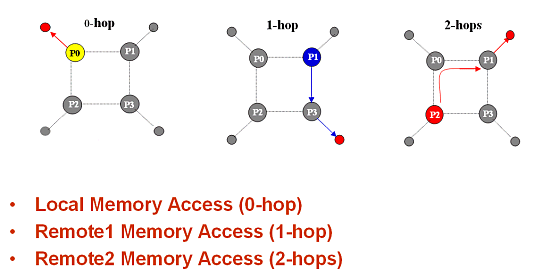 As you can see, hop is a memory access. Access to the local memory is called 0-hop. Access to the memory of the near-by processor which can be reached by the Hyper Transport bus is called 1-hop. If there are two travels on the Hyper Transport bus - it's 2-hop. Now let's have a look at the following figures (test system - Opteron 2 GHz, 128 bit memory DDR333, CL 2.5, Hyper Transport 6.4 GB/sec). Access time for:
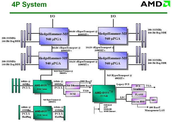
Now, when there are 4 processors, all the access times come close to the average time of 93 ns for the dual-processor system and about 118 ns for the 4-processor one. The last figure corresponds to the access time of a good uni-processor chipset. But here the total time is a sum of the memory access time and time of transfer via Hyper Transport (one or twice)! That is why such result can be considered satisfactory. Moreover, it works for the CL 2.5 memory, while for the CL 2 the figures must be lower. There are also some figures for the SUN 4-processor system which demonstrates about 207 ns when accessing the non-local memory of remote processors. So, is this NUMA or SMP? Formally, this is NUMA - the difference of 40% doesn't let us call this memory model SMP. But can we use a model for the SMP? Yes, as the difference will be smoothed away under the load - to all appearances we should add about 40 ns to these times... Thus, it turns into 140 ns against 180 ns. That is why the given system can be called SMP, and it's possible to program like for "the classic SMP", without looking back at the real architecture (NUMA). We do not exclude that later the OS will trace memory allocation in such systems - it will add up to 10% to the performance. Note that AMD uses the name of SUMO for this transient architecture. Now let's take a look at the design of multiprocessor systems based on the Hammer architecture. System on two processors: 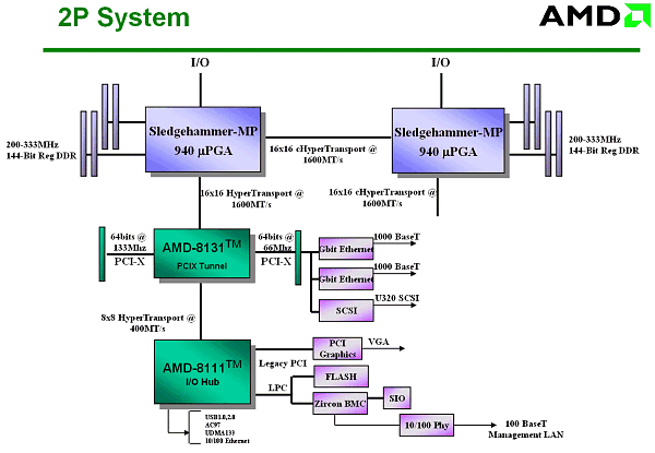 System on four processors:
 Isn't it impressive? :-) AGP is not needed here at all... The slide is quite old, that is why it doesn't have the modern Opteron's logo. By the way if we replace 4 I/O channels with 2, two free Hyper Transport connections can be attached the following way: 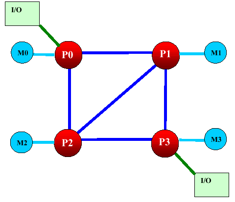 In this case the average weighted memory speed will make 19.2 GB/sec instead of 12.8 GB/sec in the classic version, and the average system "diameter" (average length of data deliveries in hops) will be 1.17 hops instead of 1.33. It will also make the delays smaller. I like this variant more than the symmetrical one because over two Hyper Transport channels of the overall performance of 12 GB/s are used very seldom. Besides, the Hammer's architecture allows assembling 8-processor systems. The four outer processors use one Hyper Transport bus each for input/output, and the central ones use their three buses as interprocessor connections. However, the delays in such system will be much higher, but I don't have exact data. The classical version looks as follows: 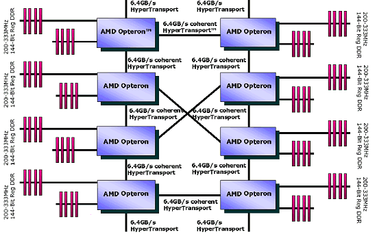 Now let's connect the pair of connections of the Hyper Transport used for the input/output. We will use diagonal outer processors. Thus we will get the average weighted memory speed of 32 GB/sec instead of 25.6 GB/sec of the classic version, and the average system diameter will be 1.64 hops instead of 1.71. However, it's possible that all three Hyper Transport buses are not coherent, only two. If it's so, the nonsymmetrical version won't be possible in the 4-processor architecture, and the 8-processor one will have no connection between the central processors, which will hike the average number of hops between the processors and, therefore, latency. I hope this rumor won't prove to be true, besides, the other sources mention that one of the controllers can switch between the coherent and non-coherent Hyper Transport. The 4- and 8-processor architectures lack for a throughput of the interprocessor connections - and with acceleration of the Hyper Transport bus the performance of SMP systems will make another jump. But it concerns future modifications of the Hammer. Obviously, the next Hammer modification will support DDRII memory (this must be a considerable performance gain). Now, when the SMP architecture of AMD is made public, it's for the market to determine its success. Is it possible to offer more than 8 processors? Yes, but now the processors' means must be coupled with the Hyper Transport switches. 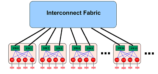 Such Hyper Transport switches are already available (for 4 buses). Switches for 8 buses are announced. If you remember, Cray has recently said it would assemble a super-computer of 36 TFlops on the Opteron processors (with the performance increasable up to 54 TFlops). Will the supercomputer's architecture resemble this picture? :-) It's still unknown, but the architecture is really powerful. Besides, the rumor has it that AMD will manufacture a special Opteron version for Cray - with four Hyper Transport links. The processors will make a 3D network. Although it mustn't be difficult to add the fourth link, it's unclear which form-factor these processors will have. I think we should place a photo of the 4-processor mainboard with the Opterons right here. 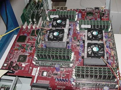 And now it's time to look at the performance. The test results reflect the ideas integrated into the architecture of the Hammer based systems. Performance. Part IBefore we proceed to the test results, let's define what performance is. On one hand - the faster, the better. Such a gauge for efficiency is really needed for the market and industry just to provide some criteria of choice. But the performance results depend on a test suite, test conditions, and a test scene in some applications (for example, in the Lightwave 7.0b). In some scenes the top position belongs to the Athlon XP, in others - Pentium 4. It's necessary to watch the test conditions very attentively and regard very carefully test results the conditions of which are unknown. It relates to all systems, not only the today's ones. Today the situation is really critical in testing various platforms. If testing one platform is a relatively simple task - there are not many variables, testing completely different systems is much more complicated and often brings very strange and incorrect results. However, this situation is not new, earlier it wasn't such obvious because the x86 platforms didn't differ much. But with time they are getting more and more different, and their test results become less comprehensible. Although the testers still measure frames, script execution time etc., there are more and more situations when the test results raise doubts. Well, it's the law of nature - as time goes on, other characteristics become more important. For example, the good old synthetic tests like CHECKIT or SYSINFO have already served their time, while some low-level tests like Cachemem are still used for measuring some or other characteristics, but the speed measured in SYSINFO doesn't reflect a CPU's speed now, does it? Then came the epoch of real tests which measured speeds in real applications. The epoch of Winstone. For a long time it represented the Ziff-Devis Benchmark... All systems were eager to get as many scores as possible - and the untainted benchmark made us sure that the test results would reflect a real speed of the system. But as the system's speed grew up, the test was becoming less adequate. Such situations when a slight change in the configuration resulted in very different results, happened more and more often. The tests which are considered the industrial standard for comparison of different architectures, such as SPEC CPU2000 (see the article) can help us. Everyone can choose those subtests from this suite which are important for him or her. But it's not simple to use them, and the results are not easily comprehensible for a novice. The industry needed a new benchmark with its results reflecting a real speed of a system in real applications. Well, the aim was reached. The new testing procedure was given a name of True Performance Initiative. Performance. Part II: TPIThe TPI technique measures performance in three aspects: Productivity, Visual Computing, Gaming. 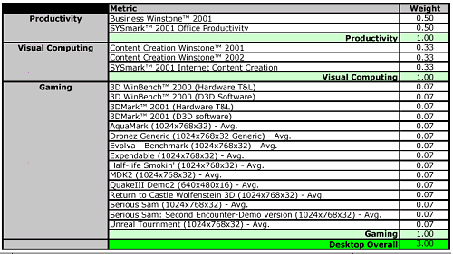 We can clearly see which applications are considered by AMD typical for measuring performance. Well, a choice of applications is the most difficult problem in developing such a test because the test results depend on the choice. AMD chose the SYSmark 2001 because it doesn't agree with the testing technique of the BAPCO SYSmark 2002. For explanations go to the SYSmark 2002 Analysis Presentation FINAL.pdf published at their site. I don't understand why they use both Content Creation Winstone 2001 and 2002 simultaneously in the Visual Computing as they almost dub each other. There are also some moot points in the games. However, the general idea is clear - they have chosen some typical user programs to test systems with the average score being the test result. Each of the tests included into the TPI is quite modern. But it's not clear what to do with Doom III - at launch this game will be one of the most popular benchmarks. Change the TPI suit? But it can result in the situation similar to the SYSmark 2002... At present, AMD plans on using the rating. If nothing has changed, the rating is based on the TPI. Here are some diagrams (I can't guarantee they are true) of the relative performance of the systems on the Athlon 64 and Pentium 4 533FSB + RDRAM PC800: 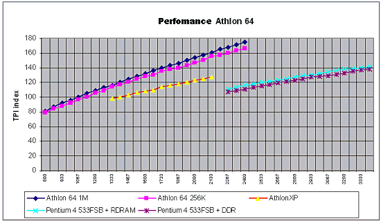 The inclination of the curve for the Athlon 64 differs from that for the AthlonXP or Pentium 4. Performance of the Hammer changes much faster with the increasing frequency - that is why this architecture wins. As you can see, the current performance level of the Pentium 4 3.06 GHz can be reached already at 1733 MHz. But the starting frequency of the Athlon 64 will probably be 1800 MHz - it seems that AMD wants some "margin of safety" so that the future 800 MHz bus of the Pentium 4 coupled with the Hyper Treading technology can't supplant the leader. However, we will know it for sure only when the processor and systems on it will be released. The diagram demonstrates the performance for systems measured with the TPI. If the Pentium 4 uses the DDR memory the graph moves downward. In this case the frequency can be even lower for the Athlon 64 to outrun the Pentium 4. However, AMD behaves tricky by using the i845D and PC2100 - with the faster memory the Pentium 4 will score higher results, probably at the level of Pentium 4 533FSB + RDRAM. The difference between the Athlon 64 256 KB L2 cache and Athlon 64 1 MB L2 cache is not very great, probably, heavier applications for workstations will have it different. Thanks to our colleagues from German magazine "c't" we have results of one more comparison: 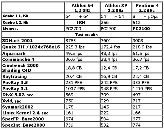 It's obviously a preproduction sample that they tested, and we don't know yet whether it will be produced in bulk. Besides, it was clocked only at 1200 MHz - I hope AMD has speedier models. The Taiwanese rumors have it that there are samples clocked at 1800 MHz. By the way, AMD played one more trick with the memory for the Pentium 4. It would be interesting to estimate the effect of attaching the 800 MHz bus and Hyper Treading to Pentium 4 - I estimate it as +15 - +20 in the TPI units. In this case the Athlon 64 processor of 1800 MHz will compete against the Pentium 4 2.53 GHz instead of 3.06GHz. However, it's not that bad. And what about workstations? AMD thinks that the following suite will be the most appropriate for them (the data are probably not precise):
At first glance, I don't know how popular these programs are among other software for workstations, as well as how reliable, just let's take on trust. However, there is no LightWave 7.0B which fancies for Intel's processors in one of the test scenes. Now look at the diagram of SPECint 2000 base (all the other diagrams refer to the Opteron processor with cache L2 1 MB): 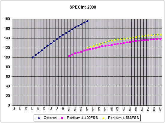 I don't understand what units are used here, that is why the data are given in the form they were obtained in. In principle, we can scale the diagram according to the figures of the SPECint 2000 for Pentium 4 of known frequencies. Also, we can use figures shown above only taking into account that they were given for the Athlon 64, and this diagram is for the Opteron. As far as I know, the performance gap between these two processor types with the other conditions being equal for the SPECint 2000 makes about 2%. In fact, the difference is caused only by the Opteron's bus of 128 bits. Besides, in this case the results from different sources are well correlated. Hence the scale factor - 100 units of the given diagram correspond to 740 units of SPECint_base 2000. By the way, there is some information that the benefit of 800 MHz FSB + Dual DDR400 in the SPECint 2000 is around 10%. If it's true, in this test the Opteron has enough reserves to compete successfully. This diagram refers to the system on the Opteron with Registered 128bit PC2100 Cas 2 memory - because usage of the PC2700 but Cas 2.5 makes the performance fall down. You can see that it makes sense to wait for the PC2700 Cas 2 memory where the performance of the Opteron system must be a little bit higher. Besides, taking into account that the inclination of the curves is different, it's sufficient to lift the frequency of the Opteron just a little for a greater increase in the frequency of the Pentium 4. For example, at 2 GHz the Opteron outruns any Pentium 4 based system with the 533MHz bus and PC800 memory. However, this diagram will change significantly with the 800 MHz bus, dual-channel DDR400 memory (this is though a rumor that relates to Intel :-)), and the Hyper Treading technology. I don't know the rating of the oncoming Opteron processors. There is information that it will start at 3400+; the series of 3400+, 3700+, 4000+ would look very logical. But this rating doesn't coincide with that of the Athlon 64 - well, it's clear as the list of tasks is different. The downside of that is that one more measuring system won't please users at all. What frequency does this rating correspond to? Some say that the Opteron with the rating of 3400+ will have its frequency around 1400 MHz-1600 MHz. But this estimation must be considered very carefully. This will get clear at the end of Q1 / beginning of Q2 after the announcement of this architecture. The diagram for the SPECfp 2000 base is not less interesting: 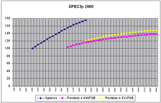 You can see that 2 GHz is enough for the Opteron to dominate. We also have information that the performance gain of the Hammer core due to the dual-channel memory is around 8%-10% for the SPECfp 2000. A certain part of the performance in the Pentium 4 architecture in the SPECfp test is on account of the Prescott core with the cache L2 1 MB and the 800 MHz bus - this market will probably have a hot competition. We don't know how much the 800 MHz will add up to the performance, but the Opteron has a good chance to remain a leader. I also heard that the performance of the Pentium 4 systems coupled with the FSB 800 MHz bus and the Dual DDR400 memory controller Pentium 4 will go up by 36% (!). If it's true, AMD might have problems in this test. For the workstations the correlation of the frequencies of the Opteron and the Pentium 4 of the comparable performance is even lower than for the desktops (it can be seen from the above ratings and frequencies) - in other words for professional applications the memory performance is more important than the frequency growth. Well, let's wait for real systems and for their competitor - Prescott. In this case Intel will need the changes (800 MHz FSB + Dual DDR400) it's going to make. Let's take a look at the performance of the multiprocessor Opteron system and compare it with the workstation based on the i850 + P4 400MHz bus. As far as I know, the data relate to the systems on the Opteron 1400 MHz revision A2 and Pentium 4 2800 MHz + RDRAM PC800: 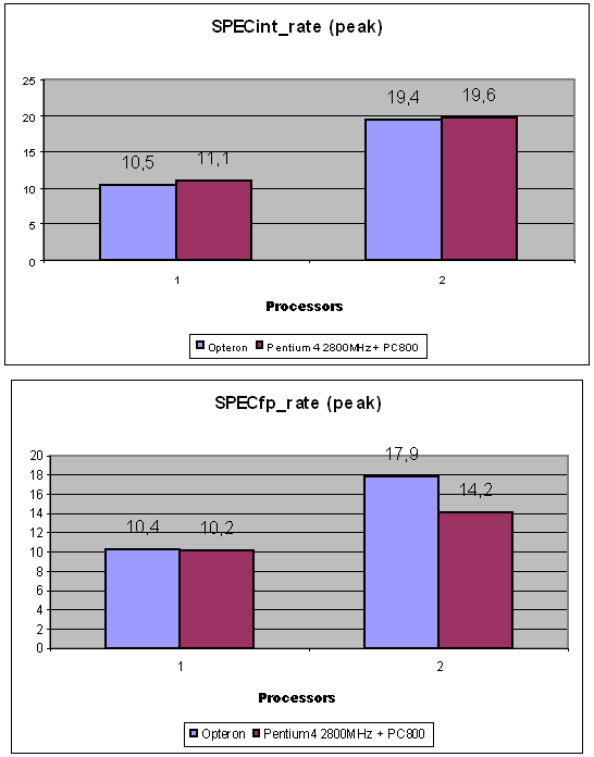 The Opteron actually managed to catch up with the processor of a twice higher frequency. And even outperform it in some aspects... Now look at the assumed performance of the Opteron in SPEC CPU 2000 in comparison with the other architectures: 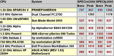 The figures given for the 2 GHz Opteron are approximate, they are extropolated from the performance of the less speedy model. As you can see, the performance level of the Opteron based system is quite good - in SPEC_fp 2000 there are only Power4 and Itanium 2 standing higher, which, however, are processors of a different level. In fact, AMD didn't mean to make the Opteron a competitor of the Itanium 2 - I just want to collate performance of two 64-bit solutions. In the integer calculations it outscores everyone, including the Itanium 2 - at least until the Pentium 4 3400 MHz + 800 MHz FSB + Dual DDR400 + 1 MB L2 cache appear on the scene. Below are some more interesting pictures. As you know, the cryptography uses a great deal of integer calculations. Data in the cryptography are of very big capacity, for example, keys 512 bits long are not seldom. That is why the integer-valued performance will have a great effect on the speed of operation of cryptographic programs. First of all, let's see how many calculations can be done after replacement of the standard x86 program with the x86-64 version: 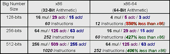 Such difference in the number of executable commands does have an effect , though here AMD gave very beautiful figures, but not entirely true. The number of commands decreased by less than 100% :-) - but let it be on account of the AMD's marketing department. The performance of such systems is also different:
 There is a slight trick because the execution times differ for the 32bit and 64bit operands, but anyway it's hard to overrate importance of x86-64 for cryptography... When the Athlon 64 and Opteron based systems appear, we will carry out big tests. ConclusionI hope AMD will start the deliveries in time and will be successful in bringing the new architecture to the market. For us it will be very interesting to watch the competition on the high-performance market after the launch of the Opteron architecture. Besides, I hope that thanks to a low cost of the layout of boards for the dualprocessor version we will get inexpensive and efficient dualprocessor systems which will become quite popular. Now AMD has an excellent marketing bait - they can widely boast of the 64bit architecture. Although the competitor also has it, the market it positions on never resorts to the tricks of such sort. :-) And a possibility to promote a 64bit processor on the mass market looks very attractive. Another interesting point is that it would be more profitable for AMD to start selling the Opteron based systems because in the very beginning quantity of the processor will be limited. In such conditions it will be more profitable to sell them at a higher price, and when the production reaches the scheduled level, they should start sales of the Athlon 64. I think that in the second quarter of 2003 the production will start but the number of the systems won't be great. Other interesting rumors are coming from Taiwan saying that AMD already has processors clocked at 2.4 GHz - note that this architecture will very likely start at 1.8 GHz (for Athlon 64). That is why, they do have some reserve for future. AMD is also said to develop a new revision supporting the DDR II apart from the DDR SDRAM. Well, I welcome this ides :-) Especially because such architecture would benefit from the accelerated memory. They also buzzing about Opteron processors with 4 Hyper Transport buses. But maybe such processors will never get to the retail market though one could use them to make 4-, 8- and more processor machines. Over 400 Athlon 64 based systems are now in different companies. Over 130 2- and 4-processor systems on the Opteron are currently tested by over 120 companies. Well, at least it shows that this architecture is interesting and that AMD doesn't need to supply samples of the new processor. I also must say that MD should keep a distance between its own systems and the competitor's ones for successful promotion of this architecture; otherwise, it makes no sense to switch to the new architecture. I'm sure that you shouldn't expect much from the Hammer architecture on the desktop market - the best performance gain will be reached on the market of SMP systems. In case of desktops the advantages are the support of the x86-64, SSE2, and more efficient models. But this is enough to attract potential customers. Links
|
Platform · Video · Multimedia · Mobile · Other || About us & Privacy policy · Twitter · Facebook Copyright © Byrds Research & Publishing, Ltd., 1997–2011. All rights reserved. |


