 |
||
|
||
| ||
|
||
|
||
| ||
Part II
System interface
Obviously, data the chip works with, programs and commands
it processes are formed by the CPU with the help of drivers,
and then they get into the graphics chip via a special graphics
bus (AGP) which acts as a system interface. Take a close look
at it: 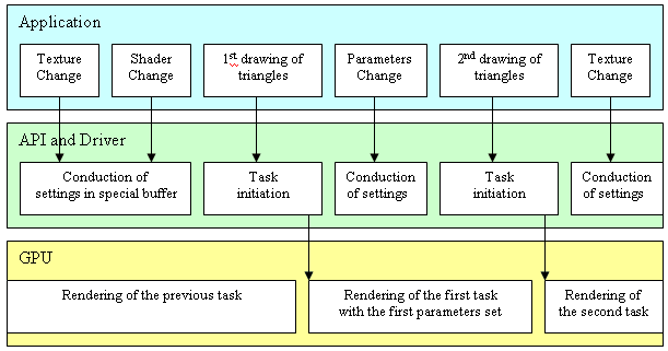 As you can see, the program addresses the API quite often changing different parameters (in modern applications changing of parameters implies primarily establishment of new textures and shaders) and then it sends a buffer with geometrical data for drawing which is to be fulfilled by the accelerator using earlier defined shaders and textures. But API requests are not sent directly to the accelerator - it would be too prodigal. Different settings are accumulated by the driver in a special buffer in the system memory, and only when the time to draw a certain geometrical picture with them comes, the accelerator is given that buffer with saved settings (commands), a shader code and links to geometrical data to be drawn. Starting from this point of time the accelerator interprets the buffer itself adjusting its internal units and draws the geometry it was given selecting data from the local and/or system memory via the system interface (the geometrical data are often located in its memory, entirely or partially). The drivers do not wait for the accelerator to complete its work, they return management to the program and keep on collecting settings and commands in a new buffer. They will have to wait only if the request for drawing comes before the accelerator finishes the previous work. By the way, it wouldn't be correct to call the data geometrical because they can have a flexible, set by the program, record format for each vertex. The record consists of a set of basic types of data - such as floating-point and integer values and vectors, color values etc. How these parameters are to be interpreted, which of them define geometrical coordinates of a pixel in space, which are the numbers of combined textures and what are texture coordinates or color values or other parameters of pixel shaders - all these issues are decided by the code of a vertex shader, by i.e. a programmer. You thus describe your internal formats of object presentation and program the accelerator so that it can interpret them correctly. The functions earlier fulfilled by CPUs are now put on the shoulders of a flexibly programmable processor. In the GeForce FX the system interface is realized via an AGP bus and, in particular, its third version. Let me sum up the differences and new features of the AGP 3.0 standard also known as AGP 8x in comparison to the AGP 4x:
Will the AGP 3.0 bring advantages for the accelerators of the
latest generation? First of all, it depends on programs. Actually,
new complex pixel shaders and nontrivial models of rendering
and lighting increases both the number of used textures and
their size and the number of parameters transferred with each
vertex which describe properties of drawn materials. Besides,
the geometrical performance of the new chip has markedly increased
compared to the previous generation, which is also going to
add requirements for the bandwidth of the system bus. But
most modern applications use scenes of moderate complexity
the textures for which can be fully put into the accelerator's
memory. And geometrical data do not take more than a third
of the bandwidth of the AGP 4x. Cinematographic quality which is so much discussed these days in connection with the GeForce FX certainly must increase demands to the system bus as so highly detailed scenes can take gigabytes. The question is how soon it's going to arrive. Most likely, more than one generation will change before we can see a scene of quality and size comparable with today's popular synthetic movies executed on the hardware level. However it can be, but the AGP 8x support is necessary as the bandwidth of the AGP 4x is not sufficient anymore. It's also necessary to comply with the modern standards and to reduce delays (when addressing the accelerator) which is becoming a real enemy today. There is nothing to worry about - the new AGP version will be enough for the GeForce FX. Probably, it is the last classical AGP in its present form - the next general-purpose graphics bus will probably be based on serial technologies developed within the frames of the 3GIO project. Memory controller and local bufferThe unexpected decision of NVIDIA to use a 128bit memory bus coupled with the high-speed DDR2 memory developed together with developed caused a lot of disputes. On the one hand:
On the other hand:
Nevertheless, I have no doubts that the experts from NVIDIA thought over their decision well. And they most likely had definite figures obtained in course of emulation or utilization of the test chips. The strongest advantage is the memory optimization technologies. Using the good controller and technologies it's possible to easier reach an effective memory throughput comparable or even greater than that of 256 bit solutions. Further we will look into this question in detail. The memory controller is based on the 4-channel scheme (4x32)
typical of NVIDIA products, which showed excellent results
on the chips of the previous generation. The internal caches
of the chip are connected to 4 memory channels and the system
bus by a full crossbar, like in the previous generation. There are 4 main data streams formed when the chip's working - three for reading (textures, frame buffer, geometrical information) and one for recording (frame buffer). Besides, a part of or all geometrical information can come from outside via the system bus. A 4-channel memory controller suits best of all for such scenario - in case of two channels the performance will drop significantly and with more channels it won't raise much though the number of chip's outputs and complexity of the board will be much greater. In this respect it's interesting to take a look at the RADEON 9500 with 64MB memory - in this configuration the R300 has only two working memory controllers, and it's quite possible that this factor is determining in its inferior performance. For cheaper versions of the GeForce FX it will be possible to have a less efficient memory but still 4 channels used in the 128 bit configuration. From the system interface and local memory interface data proceed to the chip's internal caches - a geometry chip, a frame buffer chip and a texture chip. Then they go to respective units. Let's start with the geometry: Vertex processors
The GeForce FX has three (!) independent vertex processors which fully comply (and even exceed) with the DX9 specification for vertex shaders 2.0. Even in current applications the geometrical performance of such tandem must be 2..3 times higher than that of the geometrical unit of the NV25 both thanks to the higher core's clock speed and the improved design of the execution units. But that's not all. Here is a general block diagram of the vertex processor of
the DX9: 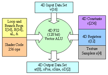 So, intermediate data are processed and stored in the floating-point
format F32. At the input the shader's program has up to 16
4D vectors - the source geometrical data we were speaking
about above. At the output we have a vertex position in the
screen coordinates, a pixel size if sprites are involved,
8 vectors of texture coordinates and 2 vectors of color values
which are then interpolated (while triangles are rendered)
for each pixel. After interpolation values of these vectors
will get into the pixel shader as input parameters. Besides,
we have 256 constant vectors assigned from outside and 12
temporary general-purpose registers used for storing intermediate
data. There are also 4 special registers - samplers which
let the vertex shader select values from textures for using
textures as displacement maps and other similar effects. From this point of view a vertex processor reminds any other general-purpose processor. But what's about programmability? A shader is a program which controls a vector ALU processing 4D vectors. A shader's program can be 256 ops long but it can contain loops and transitions. For organization of loops there are 16 integer registers of counters I which are accessible from the shader only for reading, i.e. they are constants assigned outside in an application. For conditional jumps there are 16 logic (one-bit) registers B. Again, they can't be changed from the shader. As a result, all jumps and loops are predetermined and can be controlled only from outside, from an application. Remember that this is a basic model declared by the DX9. Besides, the overall number of instructions which can be processed
within the shader with all loops and branches/jumps taken
into account is limited by 65536. What for such strict limitations?
Actually, to meet such requirements the chip can do without
any logic controlling execution of loops and jumps. It's enough
to organize successive execution of shaders up to 665536 instructions
and unroll all conditions and loops in advance in the driver.
Actually, every time the program has its constants controlling
branch and jump parameters changed, we have to load into the
chip a new shader. The R300 uses exactly such approach. Exactly
this approach lets us have only one set of control logic and
a copy of vertex program shared by all vertex processors.
And this approach doesn't make the vertex processor normal
- we can't make on-the-fly decisions unique for each vertex
taking into account criteria calculated right in the shader.
Moreover, such unrolling of jumps and loops can make a process
of replacement of the shader or its parameters controlling
jumps quite demanding in terms of CPU resources. That is why
ATI recommends to change vertex shaders as seldom as possible
- the cost of such replacement is comparable to change of
an active texture. NVIDIA made a step further making vertex processors dynamically controlled. Each vertex processor of the GeForce FX has its own indicator of a current command and a set of logic controlling jumps and loops. Such processor is more complicated but more flexible in programming. We can use newly obtained computational results as determining parameters in loops and conditions as it's done in usual programming languages for usual general-purpose CPUs. We can say that the vertex processors of the GeForce FX advocate an individual approach to each vertex. :) Such solution makes the chip more complicated but it also simplifies
the work of programmers. For example, it's not necessary to
divide an original model into several parts for loading or
for modulation to process its different parts using different
methods - one can implement necessary selection inside the
vertex shader and use just one shader instead of three-four
different ones. NVIDIA gives a good example in its documentation
for developers. Moreover, it takes quite a lot of time to
replace a vertex shader both because of checking and compilation,
and significant latency of the system AGP bus. It's possible
that it will be much more advantageous to use a big shader
consisting of several dynamically switched algorithms than
frequent changes of small and specialized shaders. Besides, it's possible to use various optimizations, for example, to calculate light from a close source by one algorithm and from a far source by another algorithm - this will also let us save on performance. We can interrupt execution of a shader, for example, according to a certain condition, to make calculations more optimized. It's interesting that the GeForce FX incorporates three vertex processors according to the number of pixels in a triangle, instead of four like in the ATI's product. Besides, in case of dynamic implementation the shaders can take a different number of clock cycles for different vertices, but new vertices are started up simultaneously, i.e. the units that have completed execution of shaders wait for those which haven't to start processing three more vertices at the same time. It's clear that dynamic jumps made NVIDIA use additional transistors. Three processors can be a weak point and a quite balanced solution - we still don't have enough information on a performance of a separate vertex processor per unit of clock speed. Like in case of usual CPUs it can differ much in different solutions. The previous tests with synthetic applications showed that NVIDIA could make perfectly balanced products. Besides, a frequency of the core of the GeForce FX is noticeably higher than that of the RADEON 9700 PRO. In the practical testing we will see how balanced the new chip is and compare it with the ATI's products. And right now let's take a glance at the comparison table of
capabilities of the vertex processors:
The parameters in bold type allow NVIDIA to speak about the support of shaders on the 2.0+ level. Of course, the dynamic execution is desired. Sooner or later all shaders, both pixel and vertex, will get it as an obligatory requirement. But now, within this generation of accelerators and API, it's not clear how popular it's going to be with programmers. What if they will use the least common denominator (like it was with pixel shaders 1.4), i.e. the base version 2.0. I think it will be so in the near future. But this new solution of NVIDIA can be supported more widely in case of OpenGL where programmers have to write two versions of a code quite often. Also remember that the set of instructions of vertex shaders in the DX9 was extended compared to the DX9, with normal trigonometric functions and conditional write and reorder instructions. It's interesting that realization of trigonometric functions in the GeForce FX is very quick - it takes the same time to calculate SIN or COS as a couple of additions (!). It seems that it operates with special matrix execution units together with big tables of constants. Here are commands supported by the vertex processors of the GeForce FX:
Reportedly, the GeForce FX won't support Displacement Maps and hardware tesselation of N-Patches. That is why the DM technology will probably suffer the same fate as the N-Patches - the support is officially provided in applications, but real models developed for it are absent. If NVIDIA's products do not support the DM, the number of applications potentially supporting it can fall down significantly. At present, the N-Patches and DM are not an obligatory requirement for the DX9 compatibility. The global tendency in the sphere of higher-order surfaces and hardware tesselation is clear — in future DX versions it will be possible to record calculated data from a vertex shader into accelerator's memory, up to generation of an arbitrary number of new vertices necessary for support of arbitrary HOS on the shader level.
Aleksander Medvedev (unclesam@ixbt.com)
Write a comment below. No registration needed!
|
Platform · Video · Multimedia · Mobile · Other || About us & Privacy policy · Twitter · Facebook Copyright © Byrds Research & Publishing, Ltd., 1997–2011. All rights reserved. |


