|
||
|
||
| ||
|
||
|
||
| ||
Part III
Pixel processors and texture units
First of all, let's again look at the logic diagram of a pixel
processor in terms of basic requirements for the PS 2.0 DX9:
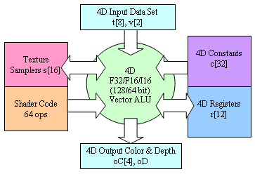 So, at the input we have 8 texture coordinates interpolated across the triangle surface (with perspective correction) and two interpolated color vectors. Originally, these vectors were calculated for each triangle vertex, but to obtain their values for each pixel rendered by a pixel shader we have to interpolate them depending on a position of a given pixel relative to the vertices. From the programmer's point of view these vectors can contain anything, not just texture coordinates and color. The pixel shader will define how to use them. At the output we have up to 4 different color values (each being a 4D vector) recorded into different output frame buffers and one depth value which we can change and record. We have at our disposal 32 constant vectors and 12 temporary vector registers. This is how pixels shaders are arranged in the R300, according to the letter of the DX9 specification, except one extension used both in the R300 and in NV30 but still not mentioned in the DX9 documentation - we can use in the shader a calculated depth buffer value and an original color value of a given pixel for realization of our own blending or for making certain decisions. In course of execution of a shader we can fulfill texture fetching, up to 16 different textures are available (the depth of nesting of dependent fetches mustn't exceed 4). For texture fetching there is a special command which indicates where to send the result, from which texture (one of 16 registers of samplers) and according to which coordinates data are to be fetched. Contrary to the previous generation this is a normal command of a shader and can be used in any place in any order. But the number of commands of fetching is limited - although the total length of a shader can reach up to 96 instructions, the number of requests to textures mustn't exceed 32 and number of other instructions mustn't exceed 64. As we have 8 coordinates interpolated across triangles, we can't call these 16 textures normal in terms for the old accelerators. If earlier a TMU was a unit including both a mechanism of texture fetch and filtering and an interpolator of texture coordinates, now there are no such TMUs. Now we have two separate units - a set of interpolators and a set of units fulfilling texture fetching by request of a shader. Multiple effects need access to different textures according to equal coordinates or, for example, multiple fetches from one texture according to dynamically calculated coordinates, that is why such approach seems to be justified. Contrary to a vertex processor which always works with the F32 data format, a pixel processor (like in R300 and in NV30) supports three formats- F32, F16 and integer I16 (R300) / I12 (NV30). The latter two formats are not just useful for compatibility with old shaders 1.x but also provide speed gains in calculations. In the DX9 the system of commands of a pixel processor is similar to the system of commands of a vertex one:
There are separate commands of texture access (fetch) and pack/unpack commands for storing nonstandard sets of scalar and floating-point variables in standard formats of textures and frame buffer. This is a good way to save on the memory's throughput and space taken by source data and shader's results when implementing complex effects. Note that recording (modification) of depth values makes unjustified all HSR optimizations and attempts of early determination of visibility which boost up performance of modern accelerators. So, if you use or modify data on depth in the shader, the hardware early HSR will be disabled, and the overall rendering efficiency will fall down. In the sphere of pixel shaders of the GeForce FX the requirements of the DX9
are exceeded again:
(*) 16 F32 registers or 32 F16 registers (**) Each used F32 constant is worth two commands, i.e. the number of constants * 2 + the number of commands do not exceed 1024. Each used F16 or I12 constant is worth one command. The GeForce FX is certainly very flexible here. But will that be needed for programmers for anything beside NVIDIA's demo programs? But we have multiple "no's" exactly for the pixel shaders. First of all, the performance of commands drops down twice (at least) while processing floating-point data compared to integer data (this is a pure computational performance without accounting for losses caused by increased data volumes). The pixel processor of the GeForce FX can execute up to two integer and one floating-point command or two texture access operations per clock — i.e. it acts as a superscalar processor in case of integer operations and reception of sampled texture values from texture units. This maintains a high speed of execution of DX8 applications with pixel shaders (for emulation of a shader of the first verion one pixel processor of the GeForce FX spends the number of clock cycles comparable with the GeForce 4). Secondly, floating-point textures cannot be filtered (!). If we want to fetch bi- or trilinear filtered values from a texture stored in the floating-pint format we must program filtering in the pixel shader using for it 4 or 8 texture fetches and a dozen of computational instructions. This must cool down our striving for increased data precision (with calculations there is only double drop). Well, there are new capabilities, but we must wait for a new edition of the chip (NV35) or a next generation (NV40) to use them effectively and without any hesitation. It's interesting that NVIDIA managed to realize texture fetching commands in
a pixel processor without any delays. Even dependent texture fetching going one
after another are fulfilled at a clock. This can give the GeForce FX a considerable
advantage over the R300 in case of complex shaders. Actually, the chip has a pool
of 8 units for unpacking, fetching and filtering of textures. Although at a clock
it's possible to fulfill two commands of data fetching from a texture in each
pixel processor, the texture values are calculated only by 8 units, i.e. up to
8 textures per clock. The second delivered value can be fetched and calculated
in advance while a pixel processor is executing other commands. For this purpose
it is kept in a special register. Each unit can fetch 8 discrete samples per clock,
i.e. implement trilinear filtering without speeding down (like in the R300). In
simple cases we get a similar picture:
However, the clock speed of the GeForce FX is higher. But real effectiveness of balancing the chip and its performance is yet to be studied. The filtering algorithms (trilinear and anisotropic) have changed in the GeForce FX. Now a use can choose between several gradations of the classical algorithms typical of the previous chips and their optimized versions, more efficient but in some cases of worse quality (it's claimed that the visual difference is minimal - the optimizations account for peculiarities of perception and orientation of polygons). A user can actually find a balance between quality and speed of filtering. Such approach is better than just integration of optimizations which can't be disabled. It's interesting that when working with traditional integer textures (8 bits
per component) values are processed by an exponential function
(gamma correction). An exponent value corresponds to the sRGB
standard. It allows saving and editing correctly an image
with a wider dynamic range, despite the 8bit data representation.
This feature is default for the DX9 chips and integrated into
the R300 and NV30. Below is an example (from ATI J) of using
such gamma correction when rendering an image: 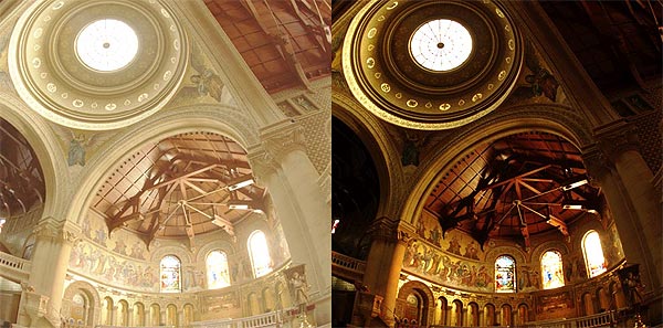 The right picture shows more typical lighting in a cathedral. And this picture was calculated using the gamma correction. The speed of trilinear filtering is crucial for modern chips. NVIDIA did nothing cardinally new here - the NV30 keeps on using adaptive algorithms of the traditional anisotropy inherited from the NV25. The developers say however that they made slight optimizations which can be enabled in the driver settings and allow for a certain performance boost without noticeable quality losses. However that can be but 16 texture units and a high core clock speed must tell upon the performance markedly. We'll see how frightful it can be for ATI products with their traditionally efficient anisotropy. The NVIDIA's approach to realization of anisotropy primarily depends on computational resources of the chip and after that on the memory's bandwidth. ATI lays the most load on the memory using the algorithm based on RIP cards. Such approach was one more argument for a 256 bit bus for ATI and a 128 bit bus with a higher clock speed of the chip for NVIDIA. Full-screen anti-aliasing and frame buffer compression
The most interesting ability of the GeForce FX is frame buffer compression, when both depth values and color values can be compressed. According to NVIDIA, the compression algorithm works without losses. It's based on the fact that in the MSAA modes most AA units in the frame buffer are not located on triangle edges and, therefore, contain equal color values. The buffer compression has a lot of advantages:
By the way, the R300 also uses compression algorithms for color information in the frame buffer, but they are not so effective. Remember the MSAA? No additional calculations are needed - all samples within the AA unit are formed from one result calculated by a pixel shader. The only factor that causes performance drops is a necessity to transfer forth and back a bigger frame buffer (according to the AA, at 4õ the frame buffer is 4 timesbiffer and at 2õ - twice bigger). At the same time, in the 4x mode most AA units have two or even one unique color value. We certainly must use such an opportunity and code effectively information of such MSAA buffer by recording only available different colors. With the MSAA we can make up for the increase size of the buffer (maybe just a couple of percent of additional data will remain). Besides, the buffer will also be compressed by the general compression algorithm. So, we can predict almost costless moderate modes of the MSAA (for example, 2x and Quincunx) and very cheap average settings (4x) in case of the GeForce FX. The advantage can be so considerable that it will be able to overlap the gap between NVIDIA and ATI products in the combined modes (FSAA+Aniso) which are the most interesting for current and upcoming applications. The GeForce FX includes a new hybrid MSAA mode named 8õ and a new hybrid MSAA mode 6xS (this one is only for DirectX). However, all these modes are just a combination of the SS and MS anti-aliasing - like in NV25, they are based on two types of base 2õ2 MSAA units - 2õ with diagonal positions of samples and 4õ, the samples are then get averaged using one or another patttern, like in the previous generation. I.e. like the NV25, the chip can record up to 4 MSAA samples from one value calculated by a pixel shader. Hence the compression ratio of 4:1. For the FSAA modes based on MSAA 2õ units this coefficient will be equal to 1:2. So, the developers of the GeForce FX counted mostly on the frame buffer and depth buffer compression, especially in the FSAA modes. In this respect, usage of the 128 bit bus can prove that the hope is justified. Dressed-up hero: GeForce FX based reference card.
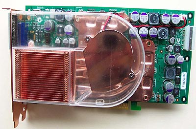
Here is a reference design of a card based on the GeForce FX:
 It houses a connector of external additional power, one DVI, one TV-Out and one VGA connector. Two Silicon Image chips control the dual-channel (up to 2048õ1536) DVI interface while the Phillips chip works with TV-Out. The GeForce FX and this card use a tried solution based on external interface chips - this is peculiar to NVIDIA's top products. In the following Mainstream products the TV-Out and DVI interfaces will probably be integrated into the chip. 8 128 MB 128 bit DDR2 memory chips from SAMSUNG, 1 GHz of effective data transfer. The memory chips are located quite far from the chip - it seems that the 128 bit bus and improved interface characteristics of the DDR2 allowed for a simpler layout. The chip is officially clocked at 500 MHz, but its future versions can have different frequencies (maybe even higher). The card can use a cooling system with external air intake and tap, like that developed by Abit:
The chip incorporates temperature sensors and a fan speed control circuit based on the chip's mode and activity of execution units. In light 3D or 2D applications the fan will have a much weaker noise level. Distribution and return: conclusion by a film criticI'm looking forward to the final scene knocking together the RADEON 9700 PRO and NVIDIA GeForce FX. The battle will take place on the arena of synthetic DX9 and real DX8/DX9/OpenGL tests. I think the most interesting scene is going to be in the extremely popular, though not finished yet, Doom III game. This game is able to influence the life of several generations of video cards of one or the other camp. NVIDIA has traditionally strong OpenGL drivers and a high clock speed of the chip, while ATI comes with a wide memory bus and a line of products which goes ahead the time. However, the preliminary data indicate that the game will have a computational character, which suits NVIDIA well. And here are some figures:
Nobody can measure effectiness of the memory optimization techniques as they can't be disabled in the drivers. But we estimate the real efficiency of these algorithms as 1.5 times for ATI and 2.0 times for NVIDIA of a physical bandwidth in typical scenarios. That is why an effective bandwidth is probably about 28 GB/s for ATI and 32 GB/s for NVIDIA, which can provide at least a 20..30% gain for NVIDIA in typical applications. Armed with these figures ATI plans on production of a chip clocked at 400..500 MHz started in the first half of 2003, which will be more affordable and not less efficient - RV350, and in the second half of 2003 we will see a .13 chip running at 500-600 MHz (R400), a future competitor against an optimized version of the NV30 (let's call it NV35). In the first half of 2003 NVIDIA will introduce two new players - NV31 and NV34 whose niche can be estimated by experienced users. The chips will be based on the mastered 0.13 fab process and use units developed for the NV30. Besides, it's possible they will release NV30 versions working at a higher core speed - 550 or even 600 MHz - in the NVIDIA's lab the first chips were running error free at such frequencies. From a user's point of view, the RADEON 9700 (not PRO) can be a very strong rival for the NVIDIA's solutions as it carries an attractive price/performance ratio for users who are not totally indifferent to games. The sphere of mid-range and budget DX9 accelerators - RADEON 9500/9500 PRO, is another question. The RADEON 9500 PRO with 128 MB memory and an undeclared 256bit bus has the most attractive price/performance ratio. At present NVIDIA has nothing to offer in this sector, but a bit later, in about three months' time we will see the NV31 solutions. The higher-level language for shaders in the DX9 will tell positively upon development of products supporting new technologies. Many programmers didn't want to deal with shaders because of too complicated development and debugging of an assembler code. The NVIDIA's initiative of creation and maintenance of an open compiler of a higher-level language for shaders (CG) and an interpreter of files similar to DX9 effects (CG FX) will have a positive effect as well. Both products have source texts available and support both APIs (DirectX and OpenGL) which will make works loads simpler for OpenGL programmers. There are plugins for popular 3D graphics packets which export models and materials in the form comprehensible for the CG FX. First samples of the GeForce FX based cards will be available in December, the mass deliveries of the chips will start in January, and in February the cards will be widely available for users. The start price is not fixed yet but in the first weeks it will be within the range from $399 (for FX 5800) to $499 (FX5800 Ultra whose paramters were shown in our comparison table). The price will certainly depend on percentage of valid chips, a situation on the memory market and a region. Now, take seats in the cinema hall - the block-buster promises to be thrilling! Moreover, I think that it will remain unpredictable till the end ... I wonder when we can have such graphics in a real-time mode
on our screens...  Aleksander Medvedev (unclesam@ixbt.com)
Write a comment below. No registration needed!
|
Platform · Video · Multimedia · Mobile · Other || About us & Privacy policy · Twitter · Facebook Copyright © Byrds Research & Publishing, Ltd., 1997–2011. All rights reserved. |