MSI FX5900-VTD128
(NVIDIA GeForce FX 5900) Video Card
and more on the Dishonest Treatment of the 3DMark 2003
|
CONTENTS
- Video card's features
- Testbed configuration,
test tools, 2D quality
- Test results: performance in the 3DMark03, drivers
v44.65
- Test results: changes in the graphics quality
in the 3DMark03, Game4
- Test results: changes in the graphics quality
in the 3DMark03, Game1
- Test results: changes in the graphics quality
in the 3DMark03, Vertex Shader
- Test results: changes in the graphics quality
in the 3DMark03, Pixel Shader
- Conclusion
The new video cards based on the NVIDIA's High-End product - GeForce
FX 5900 - have finally reached the market. However, first come not the most
powerful FX 5900 Ultra based accelerators but a bit slower ones.
The new family codenamed NV35 includes three cards: 5900 Ultra,
5900 and 5900 Value. What is the last product is not clear yet. The 5900
and the 5900 Ultra have the following memory size and frequencies respectively:
128MB against 256MB, and 400/425 (850) MHz against 450/425 (850) MHz.
In all other respects all three lines are identical, and the 5900
Ultra was earlier carefully studied. This and other reviews of the NV3x
based cards are listed below.
Theoretical materials and reviews of video cards which concern functional
properties of the GPU NVIDIA GeForce FX
We, as a test lab, can simply examine the card and return the verdict
judging by the card's capabilities, but it seems that both leading chip
makers, ATI and NVIDIA, have no shame and raise the the price for High-End
products up to $450-550, though it was $100 less a short time ago. We do
understand that memory and PCBs are expensive and it's not cheap to develop
chips that go through thick and thin and through numerous improvements,
castrations, optimizations etc., but still... are the new accelerators so
good that a piece of textolite covered with tears and sweat of workers from
the USA, Canada and China is worth so much money?
This is a very complicated and painful question, and the answer won't
be simple. But we will try to give it today.
The focus, however, will be on the fruit of collaboration of NVIDIA
and FutureMark in the light of the "peaceful" agreement according to which
all actions of the programmers at NVIDIA aimed at boosting the GeForce FX
performance in the 3DMark03 are considered to be optimizations rather than
cheats. We will look at how the FX 5900 works on the drivers' latest beta
version 44.65, and compare its speed to the FX 5900 Ultra and RADEON 9800
PRO.
Attention! This review will be followed by a review of a similar
card but from ASUSTeK where the FX 5900, 5900 Ultra, and RADEON 9800 PRO will
be compared in the game tests.
Now let's return to the card which obviously belongs to the High-End
class:
It's impossible to resist the beauty of the sparkling heatsink,
I even got up early in the morning to caress the half-sun with the first
rays of the real sun :-)).
MSI (Micro-Star International) is well known on the market. This
Taiwanese company has a wide range of products from mainboards to optical
drives. This is an old and faithful ally of NVIDIA, and it used almost all
NVIDIA's processors in its video cards.
MSI is also ahead of many NVIDIA's partners with the supplies of
the FX 5900 based cards. The card is also equal in price to the previous
solution FX 5800 (non-Ultra).
Card
| MSI FX5900-VTD128 |

|
|
AGP x8/x4/x2 interface, 128 MB DDR SDRAM in 8 chips on the front and back
PCB sides.
|
| MSI FX5900-VTD128 |
|
Hynix memory chips of 2.2ns access time, which corresponds to 454 (908) MHz.
The memory works at 425 (850) MHz, the GPU runs at 400 MHz. 256bit memory interface.
|

|
| Comparison with the reference design, front view |
| MSI FX5900-VTD128 |
Reference card NVIDIA GeForce FX 5900 Ultra |

|

|

|
| Comparison with the reference design, back view |
| MSI FX5900-VTD128 |
Reference card NVIDIA GeForce FX 5900 Ultra |

|

|

|
|
Here are some aspects to be pointed out:
- The MSI's design differs a little from the reference 5900 Ultra card, - the
right section that controls the power supply is redesigned. I heard that NVIDIA
released a new reference design with a shorter PCB and some components replaced.
MSI probably used this design. In general, the card is as long as the GF4 Ti 4600
(NV25):
- The memory size was cut down from 256MB to 128MB - on the backside there are
empty space for missing BGA chips. But the 256bit bus wasn't shortened because
the card has 8 32bit memory chips (256 bits in all). The card just doesn't support
the dual-bank memory mode.
- In general, the PCB is sophisticated, - you can see it from the photos.
Now let's have a look at the cooler.
| MSI FX5900-VTD128 |
|
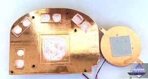
The cooler consists of the bigger and smaller parts: the former is used for
the GPU and the memory chips above, while the latter is attached to the backside
against the place where the processor is mounted.
The bigger cooler, which is extolled above is made of copper and well adjusted
for the card's configuration. There are 6 clips to hold it there!
The small cooler is rather a victim of fashion than a real necessity. What's
the use of a cooler which is pressed to the backside with a rigid thermal element
when there is a heap of logic elements between this cooler and the textolite?
It's almost useless. Also, if you look at the last photo in this table, you will
see that this piece of decoration can make problems if you try to insert such
cards into mainboards where the north bridge is turned at 45 degrees and placed
too close to the AGP slot. For example, almost all i875P based boards have such
configuration. You have to turn back the north bridge's heatsink's pins to let
the small cooler of the video card get through. And what if a north bridge has
a cooler with a fan and decorative grills?
Howeve, you can take off this small cooler, that is why this problem is not
critical.
|
|

|

|

|

|
The GPU hides under the big heatsink:
as we can see, this is the production card's marking; the chip was produced
on the 19th week of 2003 (approx. the beginning of May). The package is FlipChip,
and the die is covered above with a protective lid. A while ago we took off the
cover from the NV30 (FX 5800), and can show you how it looks inside:
The card is equipped with the Philips 7114 codec to control the VIVO:
The box contents:
|
| MSI FX5900-VTD128 |
|
The accessory pack is luxurious! There are 11 (!) CDs with different
software (see the photo on the right), including games and simply interesting
programs. Certainly, some of the discs contain drivers, utilities and Video-In
software. Also, you can find there S-Video-to-RCA and DVI-to-d-Sub adapters,
a VIVO splitter, a user guide, a company's notebook and a PC case sticker.
|

|

|
|
The card ships in the retail package.
|
|
The software suite that MSI ships with its cards was described in the GeForce
FX 5600 based card review.
Testbed and drivers
Testbed:
- Pentium 4 3200 MHz based computer:
- Intel Pentium 4 3200 MHz CPU;
- DFI LANParty Pro875 (i875P) mainboard;
- 1024 MB DDR SDRAM;
- Seagate Barracuda IV 40GB HDD;
- Windows XP SP1; DirectX 9.0a;
- ViewSonic P810 (21") and ViewSonic P817
(21") monitors.
- NVIDIA drivers v44.65/44.03.
VSync off, S3TC off in applications.
Cards used for comparison:
- Reference card NVIDIA GeForce FX 5900 Ultra (450/425 (850) MHz,
256 MB);
- Sapphire Atlantis RADEON 9800 PRO (380/350 (700) MHz, 256
MB, driver 6.343/6.360);
- Hercules 3D Prophet 9800 PRO (RADEON 9800 PRO, 380/340 (680) MHz,
128 MB, driver 6.343/6.360).
Test results
Before we start examining 2D quality, I should say there
are no complete techniques for objective 2D quality estimation because:
- 2D quality much depends on certain samples for almost all
modern 3D accelerators;
- Besides videocards, 2D quality depends on monitors and cables;
- Moreover, certain monitors might not work properly with certain
video cards.
With the ViewSonic P817 monitor and BNC Bargo cable the card showed excellent
quality at the following resolutions and clock speeds:
|
| MSI FX5900-VTD128 |
1600x1200x85Hz, 1280x1024x120Hz, 1024x768x160Hz (nothing wrong
with the quality!!) |
|
Test results: performance in 3DMark03
Conventional signs: ANISO 8xP - Anisotropic 8x Performance (earlier
it was called Balanced), ANISO 8xQ - Anisotropic 8x Quality, ANISO 16xQ
- Anisotropic 16x Quality.
The other day Aleksei Nikolaichuk published the article devoted to cheats in the 3DMark.
He carefully described what the programmers at NVIDIA and ATI do with 3DMark2001,
in particular, shader replacement. The problem is deeply studied. In short, today
all testers actually measure a degree of smartness of the guys at ATI and NVIDIA
as well as of FutureMark instead of estimating cards' performance in the 3DMark.
FM turned out to be a prostitute. If it's so simple to
replace shaders and the developers keep silence, what can we call it yet? That
concerns 3DMark2001. Strangely enough but they started protesting against cheats
only in the 3DMark03. At the same time it turned out that NVIDIA wasn't a beta
tester anymore as the company didn't want to pay through the nose every year.
The guys at NVIDIA were denounced by the world community, and FutureMark released
a patch where all NVIDIA's tricks were allegedly done away with. ATI was also
blamed a little. It reminds me Mark Twain's Tom Sawyer when Tom's Aunt suspected
him of all faults, while his brother was just a little reproved. NVIDIA was getting
more violent and tougher regarding the 3DMark03.
Suddenly... Aunt made it up with nasty Tom, and Tom even bribed
Aunt (who became the beta tester of the future 3DMark), and the latter forgave
all sins and faults and called it just innocent pranks. It's clear that
Tom will keep on playing his tricks.
So, NVIDIA and FutureMark signed a peaceful agreement where they
defined all earlier found cheats as optimizations. Now comes the next driver
version 44.65. Let's see whether the guys at NVIDIA have overcome all obstacles
of the latest patch 3.30. First of all, let's estimate the speed.
3DMark03, Game1
When we tested the performance
with the patch 3.30 that disarmed all NVIDIA's tricks, the speed fell down by
20-24%. Now, the drivers 44.65 bring the speed boost by almost the same percentage.
3DMark03, Game2
There is also a little performance gain with the drivers 44.65 relative
to the 44.03.
3DMark03, Game3
It's just the same.
3DMark03, Game4
Wow! The speed with the v44.65 has immensely risen. The gain is
even greater than the gap between the v3.20 and v3.30. If you remember, in
this test the water surface quality got worse (because of the low accuracy
of calculations).
3DMark03, 3D MARKS
So, the overall performance with the patch 3.30 and drivers v44.65
got higher.
3DMark03, Vertex Shader 1.1
The optimizations didn't omit this test either.
3DMark03, Pixel Shader 2.0
Hm.. a while ago we could see the same, even the proportions were
the same. The transition from v42.* to v43.51 was followed by a good jump
in the pixel shader speed. Since no other tests with the PS load didn't have
such results, that was an obvious optimization. I think it's the same here.
The FX 5900/5900Ultra demonstrates a good speed as compared to the
others. It just falls behind a little in the shader tests, but I do not doubt
that NVIDIA will find a smart programmer for every slow shader! NVIDIA employs
so many of them! ;-)
The drivers v44.65 works wonders: the FX 5900 (non-Ultra!) outsmarts its more
expensive competitor RADEON 9800 PRO 128MB. But isn't the image quality the cost
again? Besides, as Aleksei Nikolaichuk says in his article, cheats change the effect, and the
benchmark doesn't operate as it was originally planned by the benchmark makers.
That is why we measure a degree of smartness of programmers and driver developers
rather than a real card's speed.
Where's the truth? The patch 3.30 plus the driver 44.03? Or this
tandem has also suffered from FutureMark's revenge as well? Or maybe we should
let them make optimizations on condition that the quality doesn't get worse?
What's the truth? The answer is not simple. I will try to answer it partially
today, but more about it see in our next review where the driver will be deprived
of all possible cheats.
Now comes the quality issue.
ATTENTION! The full-sized
screenshots are recorded in the BMP format! EACH SCREENSHOT IS 5.5
MB and packed into a RAR archive of the size varying from 1.7 to 3.2 MB!
Test results: quality in 3DMark03 v.3.30, Game4
|
| Example 1 |
| RADEON 9800 PRO |
GeForce FX 5900 |
| Driver 6.343, 1600x1200 |
Driver 6.360, 1600x1200 |
Driver 44.03, 1600x1200 |
Driver 44.65, 1600x1200 |
|

|

|

|

|
|

|

|
| RADEON 9800 PRO, 6,343 vs 6.360 |
GeForce FX 5900, 44.03 vs 44.65 |
| Animated GIFs |

|

|

|

|
| Comparison of the full-sized BMP in the PhotoShop,
1600x1200 |

|

|
| Example 2 |
| RADEON 9800 PRO |
GeForce FX 5900 |
| Driver 6.343, 1600x1200 |
Driver 6.360, 1600x1200 |
Driver 44.03, 1600x1200 |
Driver 44.65, 1600x1200 |

|

|
|
|
| RADEON 9800 PRO, 6,343 vs 6.360 |
GeForce FX 5900, 44.03 vs 44.65 |
| Animated GIFs |

|

|
| Comparison of the full-sized BMP in the PhotoShop,
1600x1200 |

|

|
| Comparison with the Reference picture |
| RADEON 9800 PRO |
GeForce FX 5900 |
| Driver 6.343 |
Driver 6.360 |
Driver 44.03 |
Driver 44.65 |
| 1024x768
|
1024x768
|
1024x768
|
1024x768
|
| Reference picture, 1024x768 |

|
| Driver 6.343 vs reference |
Driver 6.360 vs reference |
Driver 44.03 vs reference |
Driver 44.65 vs reference |

|

|

|

|
|
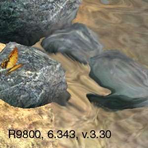
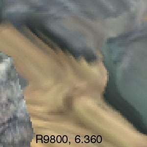
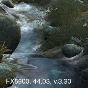
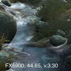
As we mentioned above, in the Game4 of the 3DMark03 3.20 the FX5xxx family
used the lower accuracy of calculations to draw the water surface, and the picture
was deformed (that was shown in this review). The patch 3.30 returns
the previous quality level. The drivers 44.65 do not cause such quality degradation
anymore. But it's obvious that the shaders were changed again. You can see it
on the animated GIF and when comparing the BMP. There are definitely some changes.
But in which direction? The question is not simple. We used the reference pictures
for comparison though we understand that every accelerator uses its own approaches
to form scenes; but anyway, it's interesting to see what's the difference. The
picture on the drivers v44.03 is farther from the reference one than that obtained
with the drivers v44.65. It turned out that the version 44.65 brought the FX5900
closer to the reference, right? Well, the comparison proves that. But does this
comparison indicate cheats, and is FutureMark right saying that the patch 3.30
and the driver 44.03 go the right way? - Nobody knows that yet.
Unfortunately, we couldn't get the 1500th frame with the reference
rasterizer (because of too lengthy calculations which ended with errors at
that).
Let's use the AntiDetect to make the
driver unable to detect applications, and compare the picture the GeForce FX 5900
renders with the "unbiased" driver.
|
| GeForce FX 5900: Comparison with the pictures obtained
with the Antidetect enabled! 1024x768 |
| AntiDetect |
Reference |
Driver 44.03 |
Driver 44.65 |

|

|

|

|
|
The pictures do differ from the reference one, that is why the picture
obtained with the software rasterizer couldn't be considered reference.
But why does the picture on the drivers v44.03
and patch 3.30 also differ from the one rendered with the AntiDetect?
Not all cheats are removed? Or FutureMark brought in there new ones
for the driver detection to artificially decrease the speed? The fact is
that the benchmark developers lie saying that the patch 3.30 works correctly.
Test results: quality in 3DMark03 v.3.30, Game1
|
| Example 1 |
| RADEON 9800 PRO |
GeForce FX 5900 |
| Driver 6.343/6.360, 1600x1200 |
Driver 44.03, 1600x1200 |
Driver 44.65, 1600x1200 |
|
|

|
| RADEON 9800 PRO, 6,343 vs 6.360 |
GeForce FX 5900, 44.03 vs 44.65 |
| Animated GIFs |
| - |

|
| Comparison of the full-sized BMP in the PhotoShop,
1600x1200 |

|

|
| Comparison with the Reference picture |
| RADEON 9800 PRO |
GeForce FX 5900 |
| Driver 6.343 |
Driver 6.360 |
Driver 44.03 |
Driver 44.65 |
| 1024x768
|
1024x768
|
1024x768
|
1024x768
|
| Reference picture, 1024x768 |

|
| Driver 6.343 vs reference |
Driver 6.360 vs reference |
Driver 44.03 vs reference |
Driver 44.65 vs reference |

|

|

|

|
| Example 2 |
| RADEON 9800 PRO |
GeForce FX 5900 |
| Driver 6.343/6.360, 1600x1200 |
Driver 44.03, 1600x1200 |
Driver 44.65, 1600x1200 |
|

|

|
| RADEON 9800 PRO, 6,343 vs 6.360 |
GeForce FX 5900, 44.03 vs 44.65 |
| Animated GIFs |
| - |

|
| Comparison of the full-sized BMP in the PhotoShop,
1600x1200 |

|

|
| Comparison with the Reference picture |
| RADEON 9800 PRO |
GeForce FX 5900 |
| Driver 6.343 |
Driver 6.360 |
Driver 44.03 |
Driver 44.65 |
| 1024x768
|
1024x768
|
1024x768
|
1024x768
|
| Reference picture, 1024x768 |

|
| Driver 6.343 vs reference |
Driver 6.360 vs reference |
Driver 44.03 vs reference |
Driver 44.65 vs reference |

|

|

|

|
|
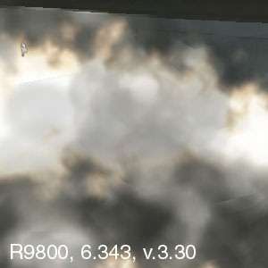
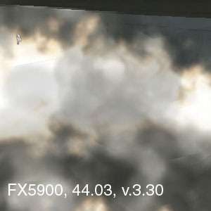
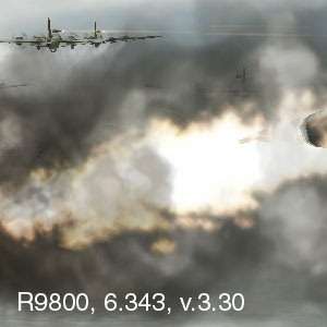
Again, NVIDIA's drivers use some cheats. This time it's connected
not with shaders, but with forced compression of semitransparent textures
which are used to form puffs of smoke. This explains the speed boost that
was seen above. The pictures of both companies differ from the reference one
and from each other. Where is FutureMark now which a while go blamed cheaters
so angrily and released the patch 3.30 where all things allegedly fell back
into place? We don't see whether the reference pictures are considered correct.
Or maybe these are not cheats but useful optimizations? But a picture must
be rendered as the developers planned, mustn't it? Where's the truth?
That is the question! Some people in the forums advocate pure, unbiased
drivers. But will that be true? I doubt it. However they will be satisfied
having fooled NVIDIA and ATI, but they forget that programmers at FM are not
less cunning.
Let's make again the driver unable to detect applications with the AntiDetect,
and look at the picture that the GeForce FX 5900 renders with such unbiased driver.
|
| GeForce FX 5900: Comparison with the pictures obtained
with the Antidetect enabled! 1024x768 |
| AntiDetect |
Reference |
Driver 44.03 |
Driver 44.65 |

|

|

|

|
|
There is again some difference from the reference picture, - why
does the picture rendered with the drivers 44.03 and patch 3.30 differ from
that rendered with the AntiDetect? Do the authors of the 3DMark03 keep their
promise?
3DMark03 v.3.30, Vertex Shader 1.1
|
| RADEON 9800 PRO |
GeForce FX 5900 |
| Driver 6.343, 1600x1200 |
Driver 6.360, 1600x1200 |
Driver 44.03, 1600x1200 |
Driver 44.65, 1600x1200 |

|

|

|

|
| RADEON 9800 PRO, 6,343 vs 6.360 |
GeForce FX 5900, 44.03 vs 44.65 |
| Comparison of the full-sized BMP in the PhotoShop,
1600x1200 |

|

|
| Comparison with the Reference picture |
| RADEON 9800 PRO |
GeForce FX 5900 |
| Driver 6.343 |
Driver 6.360 |
Driver 44.03 |
Driver 44.65 |
| 1024x768
|
1024x768
|
1024x768
|
1024x768
|
| Reference picture, 1024x768 |

|
| Driver 6.343 vs reference |
Driver 6.360 vs reference |
Driver 44.03 vs reference |
Driver 44.65 vs reference |

|

|

|

|
|
Taking into account the speed gain of the FX 5900 on the drivers
v44.65, it's obvious that the shaders are replaced.
Again we use AntiDetect to make the driver unable to detect
applications, and then look at the picture
that the GeForce FX 5900 renders with such unbiased driver.
|
| GeForce FX 5900: Comparison with the pictures obtained
with the Antidetect enabled! 1024x768 |
| AntiDetect |
Reference |
Driver 44.03 |
Driver 44.65 |

|

|

|

|
|
The question remains the same: why does the picture rendered with
the drivers 44.03 and patch 3.30 differ from that rendered with the AntiDetect?
3DMark03 v.3.30, Pixel Shader 2.0
|
| RADEON 9800 PRO |
GeForce FX 5900 |
| Driver 6.343, 1600x1200 |
Driver 6.360, 1600x1200 |
Driver 44.03, 1600x1200 |
Driver 44.65, 1600x1200 |

|

|

|

|
| RADEON 9800 PRO, 6,343 vs 6.360 |
GeForce FX 5900, 44.03 vs 44.65 |
| Comparison of the full-sized BMP in the PhotoShop,
1600x1200 |

|

|
| Comparison with the Reference picture |
| RADEON 9800 PRO |
GeForce FX 5900 |
| Driver 6.343 |
Driver 6.360 |
Driver 44.03 |
Driver 44.65 |
| 1024x768
|
1024x768
|
1024x768
|
1024x768
|
| Reference picture, 1024x768 |

|
| Driver 6.343 vs reference |
Driver 6.360 vs reference |
Driver 44.03 vs reference |
Driver 44.65 vs reference |

|

|

|

|
|
It's obvious that the GF's pictures are different on the 44.03 and
on the 44.65. The BMP comparison clearly shows that. There is no
difference between ATI's drivers.
Why? Because mathematics behind methods in different driver versions are the same, they produce the same final picture.
Let's make the driver again unable to detect applications with the AntiDetect
and look at the picture that the GeForce FX 5900 renders with such unbiased driver.
|
| GeForce FX 5900: Comparison with the pictures obtained
with the Antidetect enabled! 1024x768 |
| AntiDetect |
Reference |
Driver 44.03 |
Driver 44.65 |

|

|

|

|
And again,
the driver 44.03 plus the patch 3.30 bring a picture different from the one
drawn with the Anti-Detect.
Let's sum up the results of the 3DMark03. It's clear that NVIDIA
prefers to camouflage the speed drops in the shader operation using certain
tricks that boost the speed in the shader tests. The 3DMark03 is the most
popular for today.
There is no doubt that the methods that let spend less resources
on one or another mathematical function should be welcome. And if the guys
at FutureMark do certain things imperfectly, and NVIDIA offers a simple and
more optimal way, that is good. But in this case there is another rule that
everyone must stick to: a program must work as originally planned (though
I wish the developers showed what must be in the end). It's unfair to replace
key commands in favor of one or another video card. We thus measure not the
video cards performance but smartness of programmers.
At the same time you should remember that an end-user uses a card
on the manufacturer's drivers and no one would install drivers deprived of
such tricks. The final performance depends on the accelerator's capabilities,
drivers and such optimizations.
Soon we will take a look at one more driver deprived of detection of the applications
that users run. Aleksei Nikolaichuk has already touched upon it when studying the problem
of the 3DMark2001. We will take only the game tests and continue working on the
3DMark03.
If you are strongly against optimizations and welcome only the drivers
patched with the AntiDetect, I beg you to think again because it's really
useless.
- The driver can control the accelerator in a more optimal way than
a given application. Here is an example from Philipp Gerasimov, developer
of the RightMark 3D:
Realization of the Sin/Cos functions by the 3DMark2001 developers:
 ; c12 vecsin ( 1.0f, -1.0f / 6.0f, 1.0f / 120.0f,
 -1.0f / 5040.0f )

   ; c13 veccos ( 1.0f, -1.0f / 2.0f, 1.0f / 24.0f, -1.0f / 720.0f )

   ; c14 pis( PI, 1.0f / (2.0f * PI), 2.0f * PI, 0 )


   ; now r1.x = fAngle

   ; wrap theta to -pi..pi

   mul r1.x, r1.x, c14.y ; divide by 2*PI

   expp r2.y, r1.x ; get fractional part only

    mad r1.x, r2.y, c14.z, -c14.x ; multiply with 2*PI


   ; compute first 4 values in sin and cos series

   mov r2.x, c12.x ; theta^0 ;r2.x = 1

   mul r2.y, r1.x, r1.x ; theta^2

   mul r1.y, r1.x, r2.y ; theta^3

   mul r2.z, r2.y, r2.y ; theta^4

   mul r1.z, r1.x, r2.z ; theta^5

   mul r2.w, r2.y, r2.z ; theta^6

   mul r1.w, r1.x, r2.w ; theta^7


   ; sin

   mul r1, r1, c12

   dp4 r1.x, r1, c12.x


   ; cos

   mul r2, r2, c13

   dp4 r2.x, r2, c12.x
14 instructions in all
Here are the same functions from NVIDIA:
 ; scalar r0.x = cos(r1.x), r0.y = sin(r1.x)

   DEF c0, PI, 1.f/2.f, 2.f*PI, 1.f/(2.f*PI)

   DEF c1, 1.0f, -1.f/2.f, 1.f/24.f, -1.f/720.f

   DEF c2, 1.0f, -1.f/6.f, 1.f/120.f, -1.f/5040.f

   MAD r0.x, r1.x, c0.w, c0.y ; bring argument into -pi, .., +pi range

   EXPP r0.y, r0.x

   MAD r0.x, r0.y, c0.z, -c0.x

   DST r2.xy, r0.x, r0.x ; generate 1, (r0.x)^2, .. (r0.x)^6

   MUL r2.z, r2.y, r2.y

   MUL r2.w, r2.y, r2.z

   MUL r0, r2, r0.x ; generate r0.x, (r0.x)^3, .., (r0.x)^7

   DP4 r0.y, r0, c2 ; compute sin(r0.x)

   DP4 r0.x, r2, c1 ; compute cos(r0.x)
9 instructions in all.
It's obvious that the second way is more optimal.
-
New driver versions will bring new optimizations which will be
hidden deeper and more properly. Will one programmer be able to stand against
a whole army of guys of NVIDIA and ATI? He will until he's enthusiastic enough.
Or maybe he won't at all.
I think that we have to urge both NVIDIA and ATI to step back from
the dirty politics of twisting testers' arms with their cheats, and pay more
attention to improvement of the hardware instead of licking their errors
with drivers. The testers are actually hostages of lies and pseudo-crowns
in the 3D graphics sphere and they have to test the performance of accelerators
AS IS. Nothing is offered instead yet. You just must remember that if video
card A is faster than video card B, it can partially be on account of the
driver developers.
We can't keep silence seeing that the GPU makers
use forgery for the sake of profits and resort to all possible means to raise
ratings and speeds. We can't but agree that NVIDIA and ATI made a laughing-stock
of the testers and turned all reviews into a comedy. We insist that the policy
of cheating in the drivers for benchmarks be withdrawn, and we ask both companies
to disclose normal specifications of their products instead of showing only
what's beneficial for marketing departments.
We also wish FutureMark were less dependent on the fact
who are beta-testers among the majors and who are not, and protected its
3DMark better from the outward "invasion". The reputation of the 3DMark03
is damaged anyway.
Conclusion
As to MSI's video card tested, it's clear that this is a perfect
product regarding its build quality and accessory pack. The company takes
close to its heart production of videocards, especially of the High-End rank.
The cooling solution, and the design in general are pretty interesting.
Also remember that the FX 5900 is one of the fastest runners today.
It fearlessly competes against the RADEON 9800 PRO having the same or even
lower price. Besides, none of the RADEON 9800 PRO based cards is able to beat
the accessory suite offered by MSI.
The MSI FX5900-VTD128 can offer you:
- Excellent speed in 3D (especially with the AA and anisotropy enabled);
- Technological solution with the DX9 support (such games are
right around the corner already);
- VIVO support;
- pleasure from the high-quality product equipped with a rich
retail package (if one pays $400-420, it shouldn't be just a single card
or a card with a CD but an outwardly perfect product).
There is just a small disadvantage: it can be difficult to install
such card into some mainboards where a north bridge is located close to the
AGP port. There can be not enough place between the AGP and the north bridge's
cooler for the smaller fan on the card's backside. However, you can easily
remove this fan without detriment to the card.
Write a comment below. No registration needed!
|
|
 |
|
|
|
