Discovering DDR2-533 potential.
Results of memory module tests at the FSB frequency of 266 MHz.
|
Up to recently, DDR2-533 memory module tests (and even DDR2-667) have been carried out on mainboards based on Intel 915/925 series chipsets, their FSB operating at 200 MHz (800 MHz Quad-Pumped Bus). But the real potential of this memory type was obviously restrained, because the peak throughput of the 200 MHz FSB is only 6.4 GB/sec, while the native theoretical throughput of DDR2-533 in dual channel mode is 8.53 GB/sec. Certainly, this memory type had no such restraints when tested in single channel mode, in which it revealed its maximum potential. We already wrote about it before.
Our test lab got hold of engineering samples of the new processor Intel
Pentium 4 Extreme Edition 3.46 GHz and Intel D925XECV2 mainboard
based on recently announced Intel
925XE, which is actually a 266 MHz modification of Intel
925X. These processor, mainboard, and chipset as such will be reviewed
in a separate article. The objective of this little analysis is to
demonstrate what we should expect when upgrading from 200 MHz
to 266 MHz CPU bus in respect to memory system performance with
DDR2-533 modules operating in dual channel mode. In order to compete
this task, we'll measure the low-level characteristics of the memory
system (memory bandwidth and latency) using the RightMark
Memory Analyzer test package.
Testbed configurations
Testbed #1
- CPU: Intel Pentium 4 Extreme Edition 3.4 GHz (Gallatin core)
- Chipset: Intel i925X
- Mainboard: Intel D925XCV,
BIOS 1259 dated 08/19/2004
- Memory: 2x256 MB Samsung DDR2-533, 4-4-4-11 timings
- Video: Leadtek PX350 TDH, NVIDIA PCX5900
- HDD: WD Raptor WD360, SATA, 10000 rpm, 36Gb
- Drivers: NVIDIA Forceware 62.01, Intel Chipset Utility 6.0.1.1002, DirectX 9.0c
Testbed #2
- CPU: Intel Pentium 4 Extreme Edition 3.46 GHz (Gallatin core)
- Chipset: Intel i925XE
- Mainboard: Intel D925XECV2, BIOS 1012 dated 09/23/2004
- Memory: 2x256 MB Samsung DDR2-533, 4-4-4-11 timings
- Video: Leadtek PX350 TDH, NVIDIA PCX5900
- HDD: WD Raptor WD360, SATA, 10000 rpm, 36Gb
- Drivers: NVIDIA Forceware 62.01, Intel Chipset Utility 6.0.1.1002, DirectX 9.0c
Test Results
We used two single-type platforms based on Intel Pentium 4 Extreme Edition (512 KB L2 cache, 2 MB L3 cache, Gallatin core), Intel mainboards based on 925X and 925XE chipsets with two 256 MB Samsung DDR2-533 memory modules operating in the dual channel mode. The standard 4-4-4-11 timings scheme was used in memory system settings, which is written in the SPD module chip.
| Characteristic |
Testbed #1
(FSB 200 MHz) |
Testbed #2
(FSB 266 MHz) |
| Average real memory read bandwidth,
MB/sec |
4065
|
4498
|
| Average real memory write bandwidth,
MB/sec |
1780
|
1895
|
| Maximum real memory read bandwidth,
MB/sec |
5388
|
6366
|
| Maximum real memory write bandwidth,
MB/sec |
4267
|
5674
|
On the first platform (200 MHz FSB) the average real memory read bandwidth is 4065 MB/sec, that is approximately 63.5% of the maximum theoretical DDR2-533 memory bandwidth limited by the theoretical CPU bus throughput of 6.4 GB/sec. Upgrade to a 266 MHz CPU bus, which lifts this constraint (as its theoretical throughput is already 8.53 GB/sec, which is equal to the theoretical memory bandwidth), increases it to ~4500 MB/sec. The absolute gain is not large – just 10.6%, while the relative gain is negative (52.7% of the theoretical memory bandwidth against 63.5% on the first testbed). Still less significant absolute gain is demonstrated by the average real memory write bandwidth (1895 MB/sec against 1780, that is only 6.4%). Nevertheless, these are just "average" values, they concern the real memory bandwidth only indirectly, because they are limited by many other factors, above all – by the CPU architecture (for example, the average real memory write bandwidth tests are negatively affected by the operating peculiarities of CPU write cache).
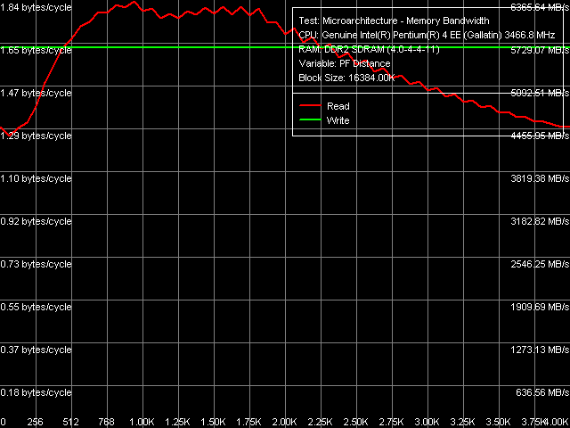
Maximum real DDR2-533 memory bandwidth,
266 MHz FSB
Proceeding to maximum values (the corresponding curves are presented on the graph), note that they are actually not particularly "maximum", because they are also limited by the CPU architecture (memory read bandwidth – by the Software Prefetch efficiency, memory write bandwidth – by the efficiency of the direct access to memory by-passing the CPU cache). Maximum real memory read bandwidth on the first platform – 5388 MB/sec (84.2 % of the theoretically maximum 6.4 GB/sec). 266 MHz bus allows to increase this parameter to 6366 MB/sec, which is higher by 18.2% in absolute value, but lower in relative value again (74.6% of the theoretically maximum 8.53 GB/sec).
Strange as it may seem, the real potential of the DDR2-533 memory bandwidth is revealed only in maximum real memory write bandwidth, which, according to our numerous tests, is strictly limited at 2/3 of the theoretical throughput of the CPU bus. We can see that in both cases – 4267 MB/sec (66.7% of the theoretical maximum) on the first platform, 5674 MB/sec (66.5% of the theoretical maximum) on the second platform. The gain reaches 32.9%, which is quite close to the expected (in the ideal case) 33.3%. So, in our first series of tests we achieved, even if it's only indirectly in one case, a victory of the 266 MHz CPU bus in the i925XE chipset over the 200 MHz modification of i925X with DDR2-533 memory operating at dual channel mode.
Memory latency
Procedures for measuring latency in Pentium 4 processors were devised,
justified, and described in detail earlier.
That's why we shall only outline them: the latency test uses pseudo-random
(as well as random) walk mode of a relatively large memory block (16 MB)
at 128 byte steps ("effective" L2/L3
cache line size dependent on hardware prefetch of adjacent line from
memory into cache in all walk modes).

DDR2-533 latency (pseudo-random and random walk),
266 MHz FSB
In fact, latency values, obtained at random walk of a selected memory block, do not have much sense because D-TLB miss value constitutes a considerable part of this parameter. Which, by the way, can be clearly seen as a difference between the latency curves for pseudo-random and random access. That's why "memory latency" will hereafter mean the latency of the pseudo-random chain walk.
| Characteristic |
Testbed #1
(FSB 200 MHz) |
Testbed #2
(FSB 266 MHz) |
Average* Pseudo-Random
Access Latency, ns ** |
81.6 |
71.7 |
Minimum Pseudo-Random Access Latency,
ns**
|
79.4 |
70.4 |
Maximum Pseudo-Random Access Latency,
ns**
|
119.9 |
110.1 |
| Average* Random Access
Latency, ns ** |
120.1 |
111.1 |
Minimum Random Access Latency, ns**
|
118.3 |
108.9 |
Maximum Random Access Latency, ns**
|
159.9 |
150.2 |
*no bus offloading
**block size – 16 MB
Average memory latency (obtained without offloading the bus by inserting "empty" operations) on the first platform, where the memory operates in asynchronous mode, is 81.6 ns. The bus being gradually offloaded, latency values are spread from 79.4 to 119.9 ns. Switching the memory to synchronous mode (the second platform) has a positive effect on the latency – it's reduced by 9-10 ns in all cases. The same picture, by the way, can be seen in case of random access latency (the same spread of values and their reduction by 9-10 ns in synchronous mode). In conclusion it should be noted that the latency values themselves are quite large. This is connected with the type of the CPU core (Gallatin, being a modified Northwood core with 2 MB L3 Cache), which does not have the most effective hardware prefetch algorithm and BIU implementation either ("cache – memory" buses).
Bottom line
Several months ago we wrote that DDR2-533
memory usage would be justified only with the appearance of chipsets
supporting 266 MHz CPU bus. According to the results of our today's
tests, this is true... but only partially, so it's high time that
we should to give a more precise definition. So, not only the FSB
frequency is important (directly connected with the throughput), but
also the efficiency of the CPU operations with memory. As you may
already know from our tests, Northwood
(Gallatin) cores do not have that highly efficient hardware and software
prefetch and BIU operations, which are demonstrated by the Prescott
core. In this connection, the real potential of DDR2-533 in the dual
channel mode will be completely revealed only with the launch of Pentium
4 CPUs on Prescott core supporting 266 MHz FSB (1066 MHz
Quad-Pumped Bus). We shall return to this issue as soon as we get
the first samples of such processors.
Write a comment below. No registration needed!
|
|
 |
|
|
|


