 |
||
|
||
| ||
|
||
|
||
| ||
On January 24, 2006 Intel presented a new mobile platform codenamed Napa, the next step in the evolution of the mobile platform Centrino. This platform has passed at least three stages in its development (if we regard evolution of the platform by the evolution of its main component — processor): from the first 130-nm Pentium M processor to the first and then to the second revision of the 90-nm Pentium M processor with Dothan core. You can easily notice that the CPU process technology was also changed (thus CPU power consumption went down as well), L2 Cache got larger. At the same time platform components changed — chipsets (from i852/i855GM/PM to i915GM/PM) and memory (from DDR-333 to DDR2-400/533), FSB frequency grew (from 100 MHz to 133 MHz, or in Quad-Pumped Bus terms, from 400 MHz to 533 MHz). What has been changed in the new Napa platform? Processor itself in the first place — the second generation of 90-nm Pentium M with Dothan core was replaced with two new processors, based on 65-nm Yonah core with a radically new name — Intel Core Solo and Intel Core Duo. It's not hard to guess that these processors differ in the number of cores in a single die: Core Solo is a single core processor, while Core Duo is a dual core modification of Yonah. This division is reflected in the title of the platform: Core Solo is still called Centrino, while Core Duo bears the title of a dual core modification of Centrino — Centrino Duo. Along with new processors, platform Napa has a different chipset — it uses a mobile modification of the i945 chipset — i945GM/PM (with integrated video and without it correspondingly) with the ICH7-M southbridge. The third important difference has to do with the first two ones and consists in increasing FSB frequency further to 166 MHz (667 MHz QP-Bus) — but not in all cases, as there are 133 MHz modifications of the new platform in the Low-End segment. Our today's analysis of low level characteristics of the processor core will deal with the most interesting modification of the Napa processor — Intel Core Duo, which peculiarity within the bounds of our review lies in using shared 2-MB L2 Cache that can be efficiently distributed between the cores depending on demands of each core. The new processor core Yonah will be compared to its closest predecessor — the second revision of Dothan core, which was reviewed earlier. CPUID dataAs usual, we'll start a review of the new processor core with examining the most significant values, output by the CPUID instruction of the processor with various input parameters. Table 1. Dothan CPUID
Table 2. Yonah CPUID
There are relatively few significant differences in CPUID data between the new Yonah core (Table 2) and the previous Dothan core (Table 1). First of all we can see that the model number is incremented by one — the new Core Duo processor with Yonah core has a model number of 14 (0xE in HEX), while the previous model bore unlucky :) Number 13 (0xD in HEX — which presumably corresponded to the first letter of Dothan). Strange as it may seem, the core stepping is still 8 (by the way, the official expansion of the core stepping C0 is not changed either — it's the same for new Yonahs as well as for the second generation of Dothan cores). It's still more surprising that the cache/TLB descriptors suffered no changes either — in other words, the manufacturer didn't invent any signs of the difference between shared 2-MB L2 Cache from the regular cache in Dothan. The changes were made to quantitative characteristics of, let's say, processor cores. Core Duo CPUID contains a number of logical cores - 2 (this parameter was undefined in Dothan). Of course, it's a tad factitious, as one can acknowledge several logical cores only if the processor supports Hyper-Threading — which is not the case with Dothan or Yonah. At the same time, CPUID clearly shows two physical cores, which is also the case with the latest dual core processors Pentium D and Pentium Extreme Edition (Smithfield core), including their 65-nm modifications (Presler core). We are going to publish results of their low level analysis in the nearest future. Along with other no less important differences, we should note SSE3 support (together with MONITOR/MWAIT instructions) as well as two "unknown" technologies (this way or another, we often come across them in our research). This time they are designated by Bits 5 and 15 Basic Features, ECX. It's natural to assume that one of these bits corresponds to the virtualization technology (VT), officially implemented in this processor. By the way, formerly unknown Bit 13 of Basic Features, ECX, which we found in the latest revisions of Prescott and Smithfield cores, is currently known (that is written in the official designation of CPUID values) as support for the CMPXCHG16B instruction, which is one of insignificant differences of EM64T from AMD64. Nevertheless, Core Duo processor supports neither EM64T as such (designated by Bit 29 of Extended Features, EDX) nor CMPXCHG16B instruction in particular. Let's wind up our examination of CPUID parameters and proceed to the results of low level tests in pre-release RightMark Memory Analyzer 3.62. The difference from official Version 3.61 lies in its capacity to detect components of the Napa platform — Intel Core Solo / Core Duo processors and i945GM/PM chipsets. Real Bandwidth of Data Cache/MemoryThe memory bandwidth versus block size curves (Picture 1) are practically identical to those for Pentium M (Dothan core, Revision C0). 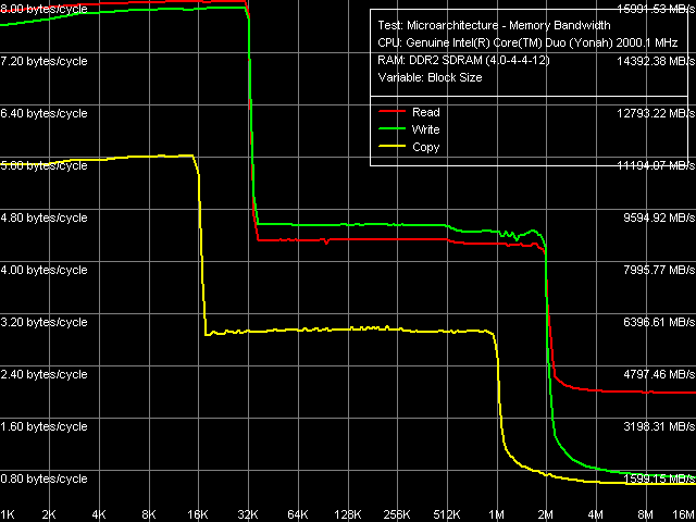 Picture 1. Average real throughput of Data Cache and RAM Indeed, "seeming" L1/L2 D-Cache sizes are 32 KB and 2048 KB correspondingly, inclusive hierarchy (when L1 Cache data must be stored in L2 Cache as well). An inflection at 2048 KB, which corresponds to the total size of shared L2-Cache, illustrates high sharing efficiency of this resource, given one of the cores has high requirements to data in memory, while the second core is practically idle. Table 3
Table 3 contains a comparison of quantitative characteristics of L1/L2 D-Cache and memory bandwidth. Proceeding from fully identical measurements of L1 Cache bandwidth in Dothan and Yonah, we can reasonably assume that this independent resource of a processor, available to each of its cores, suffered no changes in Yonah. We cannot say the same about L2 Cache. We have already mentioned many times that it's now an adaptively shared resource. Its speed characteristics of reading are nearly the same, while the cache write bandwidth got significantly larger (approximately by 40%). Considering the increased complexity of this solution, this result is more than successful. We should also note the increased bandwidth of the last and the slowest level of memory — RAM proper, both in absolute and in relative values (in terms of FSB bandwidth, which limits memory access to 4.33 GB/s for Dothan and 5.33 GB/s for Yonah). Nevertheless, we cannot say for sure whether it has to do with the increased efficiency of hardware prefetch in a processor or with the increased efficiency of the memory controller in the i945PM chipset versus the i915PM chipset. Maximum Real Memory BandwidthAs in all Intel processors, the best results for maximum real memory read bandwidth can be obtained only by Software Prefetch method (as well as reading/writing cache lines), while for maximum real memory write bandwidth - by the Non-Temporal Store method. 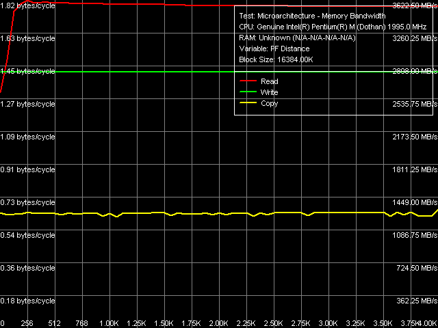 Picture 2. Maximum Real Memory Bandwidth, Software Prefetch/Non-Temporal Store, Dothan core 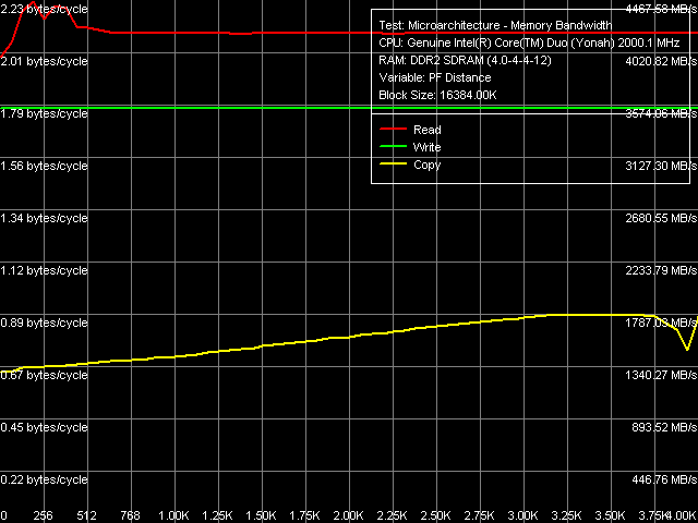 Picture 3. Maximum Real Memory Bandwidth, Software Prefetch/Non-Temporal Store, Yonah core Before we proceed to quantitative characteristics, it will be interesting to have a look at the curves obtained for Dothan (Picture 2) and Yonah (Picture 3). First of all, we can see the difference in the plot of memory read bandwidth versus software prefetch distance. In case of Dothan, prefetch quickly becomes highly efficient already at 128-byte PF distance, maximum efficiency is achieved at 256-byte PF distance. After that it goes down a little, that is prefetch remains efficient even for anticipatory reading of data on the border of the memory page (4K) with the currently read data. The situation with Yonah is significantly different: software prefetch also becomes efficient very fast (the maximum is at 192-byte distance), which is much less pronounced compared to Dothan. But the main difference consists in a noticeable drop of software prefetch efficiency when the distance exceeds 384 bytes. Prefetch efficiency drops more than twofold already at 512-byte PF distance, then it stays on a constant level up to the border of the memory page. Nevertheless, we should pay attention to the paradox plot of file copy bandwidth (using both optimization methods — software prefetch for reading and non-temporal store for writing) versus PF distance. Namely, this parameter is practically insensitive to PF distance (including zero distance, which means in RMMA that Software Prefetch is disabled) in case of Dothan, while Yonah's data copy efficiency gradually grows together with PF distance approximately to 3.5 — 3.75 KB. Then it decreases as PF distance reaches a border of the memory page. Table 4
Let's proceed to quantitative measurements (Table 4). They are practically on the same level in case of reading (FSB bandwidth is used by 84%) and writing (maximum real memory bandwidth is about 67% of the FSB bandwidth). In case of data copy operations, the maximum real bandwidth has grown from 61% to 67% of the FSB bandwidth due to noticeable changes in Software Prefetch. Average Latency of Data Cache/MemoryCommon plots of D-Cache/RAM latency versus block size (Picture 4) look quite typical. We see no significant differences from the Dothan plots. Important note: effective L2 Cache size available to a core that executes the test code is also full 2 MB. 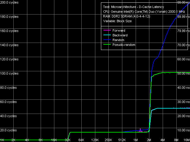 Picture 4. Data Cache/Memory Latency, 64 bytes stride size What concerns quantitative evaluations of average L1/L2 Cache and memory latencies (Table 5), we can note the most significant difference between Yonah and Dothan cores - L2 Cache latency grows from 10 to 14 cycles. Well, introduction of a much more complex control scheme for L2 Cache (efficient distribution of this resource between physical cores of a processor) cannot go unnoticed — the increase in L2 Cache latency by 4 cycles retaining (and even improving) its perfect speed characteristics is a small price. Table 5
What concerns the average memory latency in this test with effective hardware prefetch, it slightly went down (by 3 ns) in forward and backward walks, its reduction at pseudo-random and random walks is less pronounced. Minimum Latency of L2 D-Cache/MemoryAs usual, we shall evaluate these parameters by unloading the data bus by inserting empty operations between L2 Cache or memory access operators. 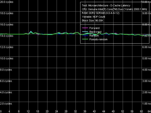 Picture 5. Minimum L2 Cache Latency, 64-byte stride The L1-L2 D-Cache unload curve (Picture 5) looks typical of P6 processors — the same curves are demonstrated by all Pentium III and Pentium M. Core Duo (Yonah) is not an exception in this respect. L2 Cache latency keeps on the constant level — 14 cycles — in all walk modes. What concerns minimum memory latency, we shall determine it in two ways — with the stride size equal to the effective line size of L1 Cache (64 bytes) and L2 Cache (128 bytes), which will allow us to evaluate the effect of hardware prefetch (efficient only in the first case) on latencies.  Picture 6. Minimum memory latency, 64 byte stride size In the first case (Picture 6), we can see practically no noticeable differences from Dothan (thus we don't publish these curves), except for the maximum efficiency of hardware prefetch is reached a tad earlier, at about 36 NOPs between neighboring memory access operators. Minimum latency of forward/backward walk reaches 10.1 ns (9.2 ns for Dothan), pseudo random - 46.9 ns (versus 48.2 ns), random - 69.0 ns (versus 72.5 ns). Thus, the new platform demonstrates no significant changes in memory access latencies with hardware prefetch.  Picture 7. Minimum memory latency, 128 byte stride size There are no noticeable differences in the second case either (Picture 7), hardware prefetch is practically idle (indicated by identity of unload curves for forward, backward, and pseudo-random memory walks). Minimum latency in this case is 87.5 ns versus 95.8 ns on the Dothan platform. We can say that these differences fully reflect the differences in memory access latencies irregardless of a processor type. Data Cache Associativity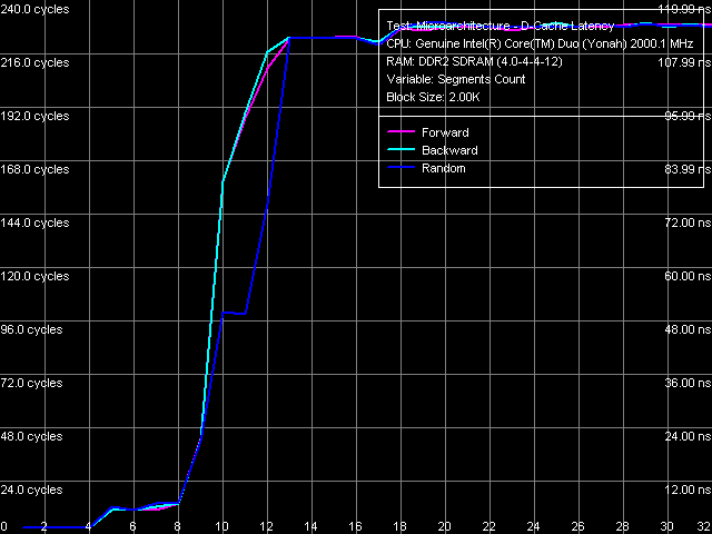 Picture 8. L1/L2 data cache associativity Yonah's cache associativity curves (Picture 8) look quite distinct. L1 data cache associativity is equal to four (not eight, as specified in CPUID descriptors), L2 associativity is eight (that is it matches the official value). The same associativity situation can be seen on Dothan core, Yonah's shared L2 Cache brings no changes into it. Real L1-L2 Cache Bus Bandwidth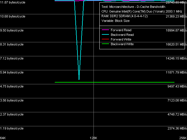 Picture 9. Real L1-L2 Cache Bus Bandwidth Real L1-L2 bus bandwidth graphs, obtained by reading whole L2 Cache lines (Picture 9), look familiar (except for an accidental dip on the backward read curve at ~112 KB). Table 6
Comparison of quantitative characteristics of the L1-L2 bus bandwidth in Dothan and Yonah (Table 6) reveals their noticeable growth in the latter. For example, read bandwidth (both forward and backward) grows to 11.87 bytes/cycle (by 9-13%), write bandwidth — to 4.91 bytes/cycle (by 52.5%). We have already seen a noticeable growth of L2 Cache write efficiency in the average L2 cache bandwidth test. Thus, we can again stress a very good implementation of the complex shared L2 Cache, which did not have a negative effect on its speed characteristics.  Picture 10. Data arrival test on L1-L2 Cache bus Capacity of the L1-L2 D-Cache bus is still 128, which is illustrated by the D-Cache arrival test (Picture 10) — a requested 64-byte cache line does not arrive via the L1-L2 bus for 3 cycles of addressing L1 Cache, so there appear additional latencies for reading the 2nd DW, which is 32 bytes or more away. I-Cache, Decode EfficiencyWe proceed to the most interesting part of our review — evaluating decode/execute efficiency of various simple arithmetic-logic operations. As is well known, the overhauled decoder (added micro-op fusion for SSE instructions and added SSE3) is just as important an innovation in Yonah core as the shared adaptive L2 Cache. 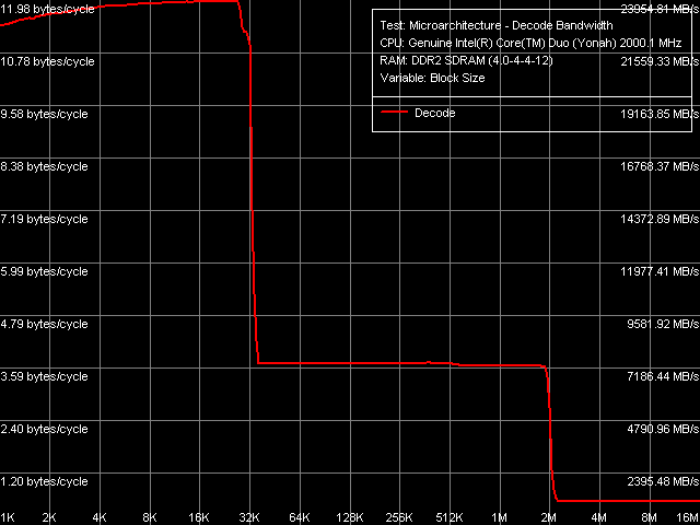 Picture 11. Decode/execute efficiency for 6-byte CMP instructions We publish the graph of decode/execute efficiency for large 6-byte CMP instructions (Picture 11) only to make sure that L2 Cache is fully available to one core even when executing a super long (up to 2 MB) code fragment from a specified processor memory area. Table 7
Nevertheless, quantitative results of these tests are more interesting in comparison with those for Dothan core (Table 7). First of all, we should pay attention to a considerable growth of execution speed for the SUB instruction sequence (sub eax, eax), XOR (xor eax, eax) and for the mixed XOR/ADD sequence (xor eax, eax; add eax, eax). It means that Intel has finally fixed the notorious problem of the P6 decoder, which couldn't resolve such false dependences. For example, all P6 processors, including the latest revision of Dothan core, executed these instructions with the maximum speed of one instruction/cycle, efficiently using only one of two available ALUs. But Yonah righted the wrong — from now on these instructions are executed as they should be - at the speed of two instructions per cycle. It brings Yonah's decoder maximum close to the decoder in AMD K7/K8 processors, which didn't suffer from this drawback from the very beginning. The second difference you may observe consists in more efficient execution of code from L1 I-Cache, which is especially noticeable with relatively large 6-byte CMP instructions (cmp eax, 00000000h) — their execution speed has grown from 11.92 bytes/cycle to nearly the maximum value — 11.98 bytes/cycle. On the other hand, we should note some reduction in the execution efficiency of code from L2 Cache, noticeable practically in all cases except for the smallest NOP instructions. Nevertheless, continuous execution of a code fragment exceeding 32 KB will hardly be necessary, so this drawback shouldn't be considered a major flaw against the background of noticeable improvements in Yonah's decoder. What concerns prefix instructions CMP (6-byte compare operations that are preceded by two single-byte meaningless prefixes), Yonah demonstrates no significant changes. Maximum execution speed for these instructions is still 4 cycles per instruction. Nevertheless, we can note a tad faster execution speed of these instructions from L2 Cache against the background reduction of its overall efficiency. 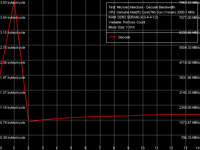 Picture 12. Decode/execute efficiency for prefix instructions NOP A more detailed picture of decode/execution efficiency for prefix instructions is provided by the cognominal test, which executes instructions of the following kind [0x66]nNOP, where n = 0..14. The overall picture of this test (Picture 12) has not changed — this situation is typical of all P6 processors, since Pentium III (probably also Pentium PRO/Pentium II — we haven't tested them). Maximum efficiency of truncating prefixes is reached only when their number is equal to one. As this number grows, decode/execute speed of these instructions drops (especially in terms of a number of instructions executed per cycle). I-Cache Associativity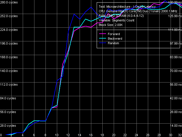 Picture 13. I-Cache Associativity The I-Cache Associativity test (Picture 13) that measures execution time of a sequence of unconditional jumps at different distances from each other (divisible by the cache segment) illustrates the 4-way associativity of L1 I-Cache and the 8-way associativity of L2 Cache. We have obtained the same result for D-Cache associativity as well as associativity of D-Cache and I-Cache in Pentium M (Dothan). Instruction Re-Order Buffer (I-ROB)Here is the main principle of operation versus the new RMMA, which allows to determine I-ROB depth: it runs one simple instruction that takes much time to execute (it uses an operation of dependent loading of a subsequent string from memory, mov eax, [eax], and right after it a series of very simple operations, which do not depend on the previous instruction (nop). Then ideally, as soon as the execution time of this combo starts to depend on the number of NOPs, the ROB depth can be considered used up. 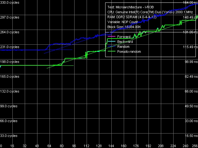 Picture 14. Instruction Re-Order Buffer Depth The result of this test for Yonah, approximated into straight lines, can be seen in Picture 14. We obtained practically the same situation for the new revision of Dothan core. Thus we can assume that the I-ROB implementation in Yonah and Dothan cores is identical. I-ROB depth in these processors, which is responsible for a number of NOPs - the cross-point of two approximating straight lines, amounts to 72 instructions. TLB CharacteristicsLet's determine the size and associativity of the D-TLB Cache. 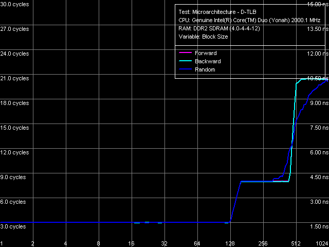 Picture 15. D-TLB size It's a standard situation (Picture 15): D-TLB size is 128 entries, buffer miss penalty is 5 cycles. Further latency increase in the area of 512 entries has to do with exceeding the limits of L1 Cache (512 x 64 bytes = 32 KB). 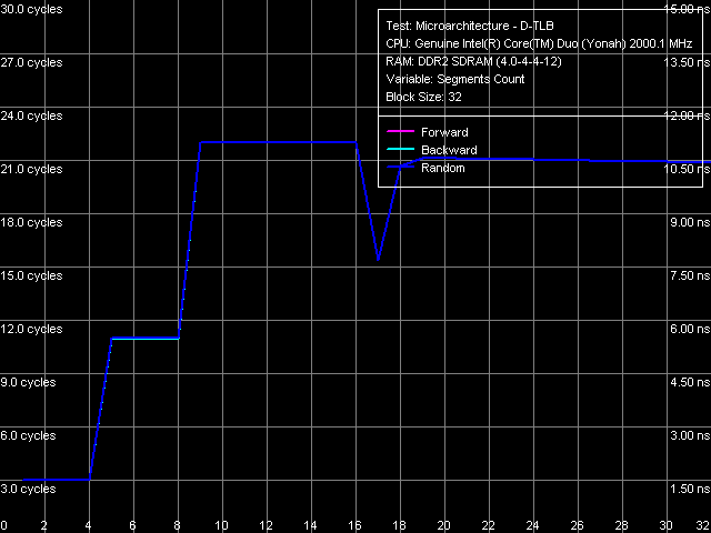 Picture 16. D-TLB associativity We have already seen D-TLB associativity (Picture 16) with two surges (which is much more typical of two-level TLB, each level has a different associativity) for the second revision of Dothan core. Early revision of Pentium M were characterized by standard curves with an only inflection at 4 segments, which corresponds to the true D-TLB associativity of processors from this family. 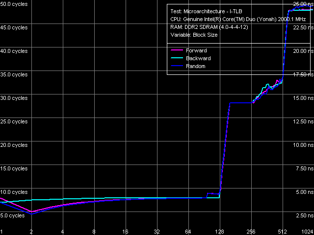 Picture 17. I-TLB size Results of measuring I-TLB size (Picture 17): 128 entries, buffer miss penalty is approximately 20 cycles. The same picture could be seen with Dothan core. 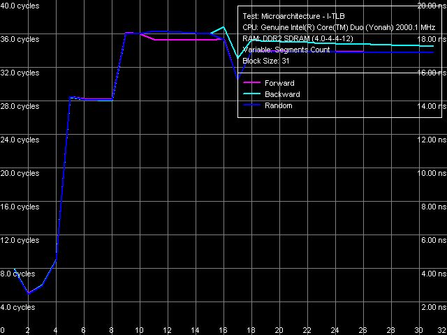 Picture 18. I-TLB associativity The situation with I-TLB associativity (Picture 18) is quite clear and corresponds to the curves we obtained earlier for both revisions of Dothan core — I-TLB associativity is 4. All the four curves (size and associativity of D-TLB and I-TLB) for Core Duo (Yonah) and Pentium M (Dothan rev. C0) look the same, which indicates identical organization of these resources in these processors. ConclusionThe analysis of main selected low-level characteristics of the dual core modification of the new Yonah core in Intel Core Duo processors produced a good impression. First of all, we should note a superior implementation of efficient distribution of the shared L2 cache between individual cores depending on their requirements. Success of this design shows not only in 100% efficient usage of the entire L2 Cache by a single core (it's a topical problem these days, when the majority of applications are still designed for a single core architecture, that is being single threaded), but also in good speed characteristics of L2 Cache and L1-L2 bus (in some cases they even exceed speed characteristics of the latest Dothan core revision) accompanied by a relatively small increase in L2 Cache access latencies. The second but no less important difference of the new Yonah core from the previous generation (Dothan) is a much improved instruction decoder. It allows not only better execution of SSE instructions (we cannot see it in our today's review). It also helps eliminate false dependencies between certain simple arithmetic-logic operations, which are really used in practice to empty registers. In other words, designers have finally fixed a number of ancient drawbacks of the P6 decoder, which has brought it maximum close to a better decoder implemented from the very beginning in AMD K7 and K8 processors.
Dmitri Besedin (dmitri_b@ixbt.com)
February 22, 2006 Write a comment below. No registration needed!
|
Platform · Video · Multimedia · Mobile · Other || About us & Privacy policy · Twitter · Facebook Copyright © Byrds Research & Publishing, Ltd., 1997–2011. All rights reserved. | |||||||||||||||||||||||||||||||||||||||||||||||||||||||||||||||||||||||||||||||||||||||||||||||||||||||||||||||||||||||||||||||||||||||||||||||||||||||


