 |
||
|
||
| ||
. The first article from the new series. April 18, Intel has announced the first dual core Pentium Extreme Edition 840 processor, based on the new core codenamed Smithfield, that supports Extended Memory 64-bit Technology (EM64T). Note that the name of the new processor lacks the habitual "Pentium 4" — this phrase is curtailed to "Pentium", though there are no doubts that Smithfield core is based on the NetBurst microarchitecture. Secondly, the new processor poses another change in the "extreme" ideology of processors with NetBurst microarchitecture. The extreme nature of the first Pentium 4 Extreme Edition processors consisted in 2MB L3 Cache. Later on, with the relatively recent launch of Pentium 4 Extreme Edition 3.73 GHz processors, this notion has become associated solely with the 266MHz FSB (1066 MHz Quad-Pumped). And the extreme nature of the new processor has obviously to do with its dual cores (because there is nothing else we can tie it to). At the same time, the future will see the launch of a new series of dual core processors from Intel under the Pentium D trademark, which will again require to review the notion of CPU extremity. Well, these are manufacturer's problems. And we are to examine the new processors and their architectural features in particular. The present article will traditionally review the key low-level characteristics of the new dual core in comparison with its previous single-core counterparts — Prescott, Nocona, and Prescott/2M cores, which were reviewed in the articles "Detailed Platform Analysis in RightMark Memory Analyzer. Part 6 — Intel Xeon (Nocona) platform" and "Detailed Platform Analysis in RightMark Memory Analyzer. Part 8 — Intel Pentium 4 and Pentium 4 Extreme Edition processors with a new revision of Prescott core". Testbed configuration
Software
CPUID Characteristics
We'll start the review of the new Smithfield core with the analysis of the most important characteristics, provided by the CPUID instruction.
So, according to the CPU signature (0F44h), the new Smithfield core can be considered a continuation, sort of a new revision of Prescott and Nocona/Irwindale cores (their latest revision N0 is signed as 0F43h). Nevertheless, Smithfield core used in Pentium Extreme Edition 840 (or simply Pentium EE 840) got the official alphanumeric revision designation A0, that is it's the first core in a series. Cache/TLB descriptors look usual, as in Prescott/Nocona cores with 1MB L2 Cache (the total claimed size of L2 D-Cache in Pentium EE 840 is 2 MB. But it's not hard to guess that this notion is quite relative, because L2 Cache is an isolated but not a shared resource for both cores — 1 MB per each core). Extended features of the processor offer nothing principally new either. You can easily notice that the new core supports neither Thermal Monitor 2 nor Enhanced Intel SpeedStep (Demand-Based Switching), or Execute Disable Bit. However it completely supports Extended Memory 64-bit Technology (EM64T) as well as Enhanced Halt State C1E (it cannot be presented in CPUID data). The presence of two unknown technologies is also a usual thing (we have assumed they are LaGrande and VanderPool), designated by the 2nd and 13th Basic Features bits, ECX register. Thus, according to its key characteristics, the new Smithfield core ranks somewhere between the latest Revision E0 of Nocona core (if we take it without TM2 and DBS technologies) and the extreme version of Prescott/2M core, implemented in Pentium 4 Extreme Edition 3.73 GHz, but with 1MB L2 Cache and disabled XD bit. Nevertheless, the main difference on the processor level has to do with the number of logical processors, designed in a single physical package (in the package, not in the core) — it has grown to 4 (each physical core is represented by two logical processors, due to Hyper-Threading support). Real Bandwidth of Data Cache/MemoryLet's proceed to the results of the new processor in the latest RMMA pre-release 3.5. When we tested the new processor, the SysInfo component of the test did not properly support this processor and the chipset yet. Consequently, this processor is identified as a regular Intel Pentium 4 540 (it's actually true in terms of the clock and L2 Cache size for each core — if we pretend not to notice the dual core and EM64T support). When the program tries to write out timing values by configuration registers of the i955X chipset according to the official documentation, there occurs an error in tRAS — it turns out twice as low compared to the true value (which probably has to do with a mistake in the documentation). Nevertheless, these shortcomings are already corrected in the coming release (Version 3.5) of this test package.
The general picture of real memory bandwidth (L1/L2/RAM) on Pentium EE 840 is shown below.
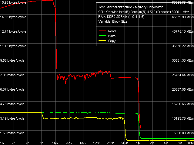 Real Bandwidth of Data Cache and Memory Pentium EE 840
You can see the following key features on the graph: indeed, L2 D-Cache size is 1MB (that is there can be no intrusion of L2 Cache from the neighboring core), but the memory bandwidth of this level slumps noticeably already at 256 KB blocks. It has to do with the D-TLB depletion, which size is still 64 entries, that is 256 KB of covered virtual address space. No differences in L1 and L2 Cache write efficiency (there is no typical inflection at 16 KB) indicate the Write-Through organization, implemented in all previous cores of Pentium 4/Xeon processors.
Quantitative characteristics of L1 and L2 D-Cache bandwidth in Smithfield match the previously obtained characteristics of the latest Prescott/2M core revision — we should note a higher read efficiency of L2 Cache compared to the earlier revisions (D0) of Prescott/Nocona cores. More prominent changes can be seen in average real memory bandwidth. While the real memory read bandwidth has grown insignificantly compared to Pentium 4 660, the real memory write bandwidth has grown quite noticeably (approximately by 20%). As usual, it can be a result of improved BIU interface of the core or an improved memory controller in the new i955X chipset. Maximum Real Memory Bandwidth
As usual (for Pentium 4 processors), Software Prefetch method allows maximum memory bandwidth, while other methods are not so highly efficient.
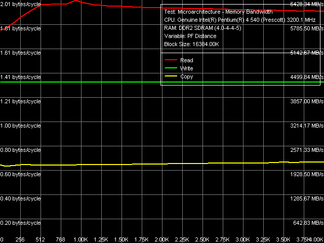 Maximum Real Memory Bandwidth, Software Prefetch, Pentium EE 840 The curves of real memory bandwidth versus software prefetch distance in Pentium EE 840 are typical of Prescott cores (they match those we obtained on previous revisions of this core). I want to note a smoother decrease of values relative to the maximum as the prefetch distance is increased. Most likely it has to do with the improved memory controller in the i955X chipset rather than the prefetch as such.
This assumption is also backed up by high (compared to the previous reviews) maximum real memory bandwidth, obtained with other methods that do not involve software prefetch, especially the cache line read method (memory bandwidth values in this case are just a tad lower than the theoretical limit).
The most striking changes can be seen in maximum real memory write bandwidth. Of course, Non-Temporal Store method allows to get 2/3 of the maximum theoretical FSB bandwidth in all cases, no more, no less. The cache line write method has grown noticeably more efficient on the new platform — the obtained memory bandwidth values amount to approximately half of the maximum theoretical value. It's again the effect of the improved memory controller in the new i955X chipset. Data Cache/Memory Latency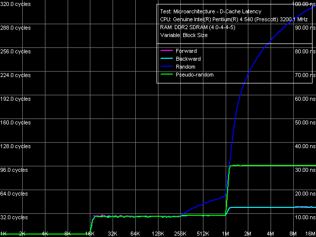 Data Cache/Memory Latency, Pentium EE 840
Typical features of Data Cache and D-TLB organization are no less clear in this test: 16 KB and 2MB inflections, which correspond to L1 and L2 Cache sizes, as well as a smooth rise of random L2 Cache access latency with the block size starting from 256KB.
Quantitative latency characteristics of L1 and L2 Cache are the same for all processors included into the table. Concerning the memory latency, the table values have been obtained in a separate test, where the data chain is walked at 128byte steps, i.e. the effective L2 Cache line size. It's not hard to notice that the average memory latencies in all walk modes on Pentium EE 840 platform are almost no different from the latencies obtained on Pentium 4 660 platform. A slightly lower random access latency (101 ns versus 106 ns), when the hardware prefetch algorithm is nearly idle, can serve as an additional sign of an improved memory controller used in the i955X chipset, which we have mentioned above several times. Minimum Latency of Data Cache/Memory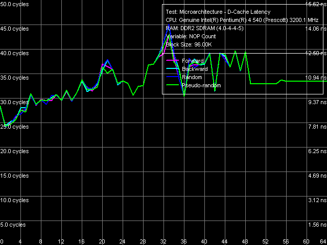 Minimum L2 Cache latency, Pentium EE 840, Method 1 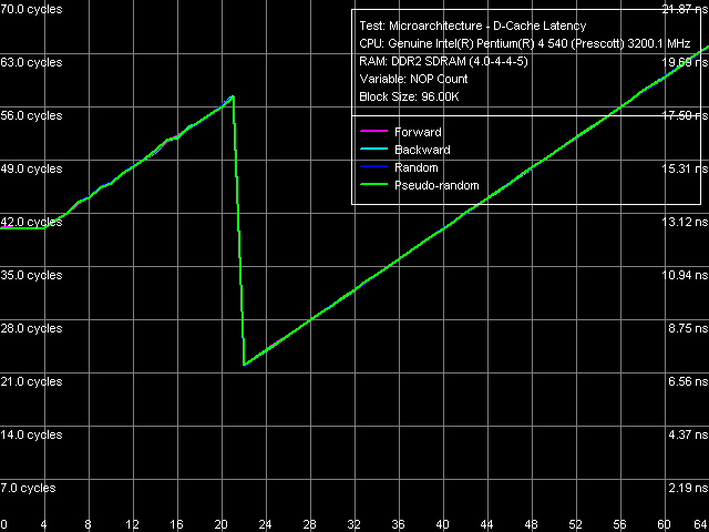 Minimum L2 Cache latency, Pentium EE 840, Method 2
The L1-L2 bus unload curves, that is the minimum L2 Cache latency in Smithfield core, look as usual. They are similar to the curves, previously obtained on Prescott cores: latency of this level obviously does not reach its maximum at standard L1-L2 bus "unloading" by inserting "empty" operations (Method 1), and it goes down to 22 cycles at "non-standard" unloading, specially developed for processors with pronounced speculative data loading (Method 2).
 Minimum memory latency, Pentium EE 840
L2-RAM bus unload curves for the Pentium EE 840 processor also look usual.
Minimum memory latencies, obtained with the sufficiently unloaded L2-RAM bus, turn out somewhat lower compared to the Pentium 4 660 test results. Considering that the buses on these processors are unloaded in absolutely the same way (unload curves, so to speak), this phenomenon should be again attributed to the improvement of a memory controller in the new chipset. Data Cache Associativity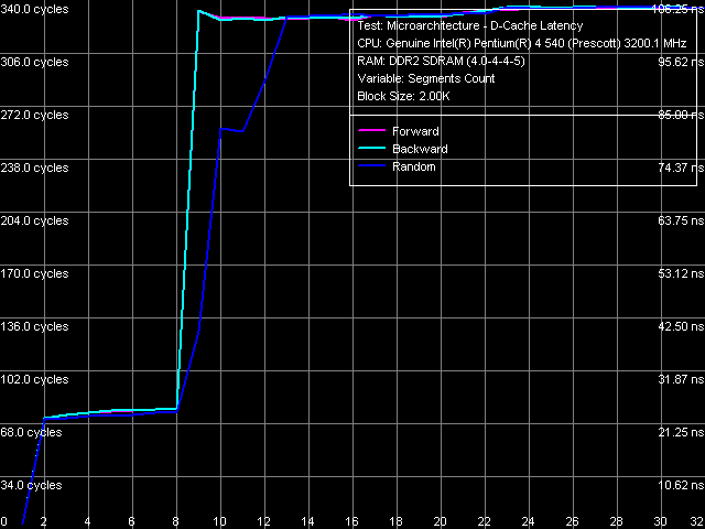 D-Cache Associativity, Pentium EE 840 L1/L2 D-Cache associativity test for both processors, which result is shown on the picture, again indicates the lack of any changes in this parameter. As in all the other reviewed Pentium 4/Xeon processors on Prescott and Nocona cores, the "effective" L1 data cache associativity is equal to 1, associativity of the integrated L2 instruction cache/data cache is equal to 8. L1-L2 Cache Bus Real Bandwidth
In comparison with the previously reviewed Prescott/2M core revision N0, which demonstrated noticeably lower results in this test compared to the earlier core revisions, the new Smithfield core revision A0 gives us a pleasant surprise in this test. Namely, not only the real L1-L2 D-Cache bus bandwidth returned to the previous values, usual for Prescott cores, but even grew a tad higher. Thus, the reason for slumped values on Pentium 4 660 has become obvious — it has to do with the L2 D-Cache, increased twofold. As soon as it was decreased to 1MB per core (in Pentium EE 840), everything fell into place... and even a tad higher :). Trace Cache, Decode/Execute Efficiency
Let's examine another interesting component of the NetBurst microarchitecture - its specialized cache for micro-operations (Execution Trace Cache) provided by the predecoder.
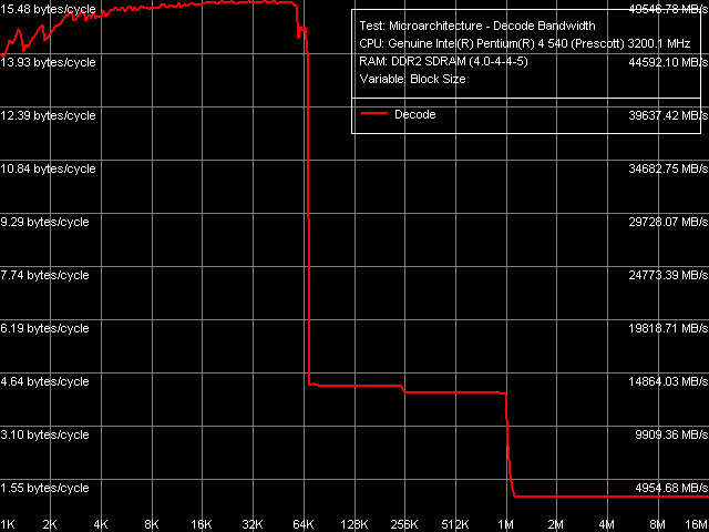 Decode/execute efficiency, Pentium EE 840 As always, the overall picture of decode/execute speed for "large" 6-byte CMP instructions is the most illustrative. This test, as well as all the other tests of this type, demonstrates no qualitative differences in the behaviour of Smithfield core under review and the previously tested Prescott/Nocona cores. So, let's proceed to the qualitative evaluation. Decode/execute efficiency, Xeon (Nocona D0)
Here is a log of our research to track the mysterious and interesting tendency of Execution Trace Cache changes. At first, let's have a look at the data, previously obtained on Xeon platform (Nocona core, Revision D0). This processor core, equipped with EM64T, was the first to show the deterioration tendency for decode/execute efficiency of some commands - in particular, simple operations like TEST (test eax, eax) and CMP 1 (cmp eax, eax). For your convenience, the results that suffer changes in the next cores are marked with red. Decode/execute efficiency, Pentium 4 660 (Prescott N0)
The outlined tendency of CPU performance deterioration (execution of some commands) carries on its development in Prescott/2M core revision N0 (Pentium 4 660 and Pentium 4 Extreme Edition 3.73 GHz). First of all, we can see the subsequent decrease of TEST and CMP 1 execution efficiency. The second significant modification is the reduction of maximum execute speed for all CMP operations from L2 Cache to 4.0 bytes/cycle (1.0 or 0.67 instructions/cycle, depending on the command length) as well as prefixed CMP to 4.14 bytes/cycle (0.52 instructions/cycle). Decode/execute efficiency, Pentium EE 840 (Smithfield A0)
Let's proceed to the data obtained on the latest Pentium EE 840. Nothing has changed with TEST and CMP 1 — their execute efficiency from Trace Cache is the same as in Prescott/2M based processors. But the execute efficiency of CMP3-CMP6 as well as prefixed CMP1-CMP4 operations from L2 Cache has grown higher again, even a tad higher than Nocona. Does it ring any bells? We have just seen a similar picture in the previous test — Real L1-L2 Cache Throughput. It has obviously to do with it. It's clear now: the drop in execution performance of some large instructions from L2 Cache on processors with 2MB Prescott cores (Revision N0) is the result of enlarged combined L2 Cache for instructions/data.
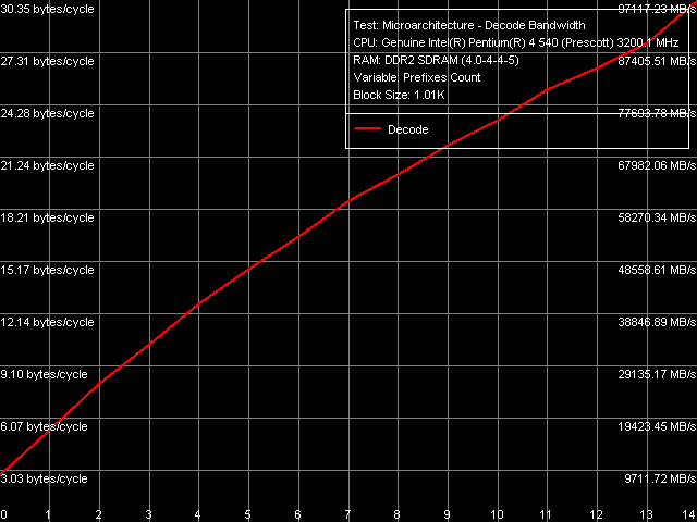
The second significant efficiency deterioration of the decoder/pipeline in Prescott/Nocona cores with EM64T was in the decreased efficiency of truncating "meaningless" prefixes in the test that executed instructions of the type [0x66]nNOP, n = 0..14.
 Decode/execute efficiency for prefix instructions, Pentium EE 840
Note that the new revision of Prescott N0 cores with EM64T has very little changes in this respect: it's an unaccountable but easily replicable "slump" in case of 13 prefixes sharp before the NOP instruction. You can easily see that the same peculiarity pertains to the new Smithfield core as well. TLB Characteristics
We shall not go into the analysis of D-TLB and I-TLB characteristics, considering that they (by CPUID descriptors) match in all processors under review.
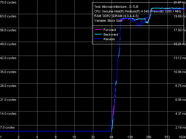 D-TLB size, Pentium EE 840 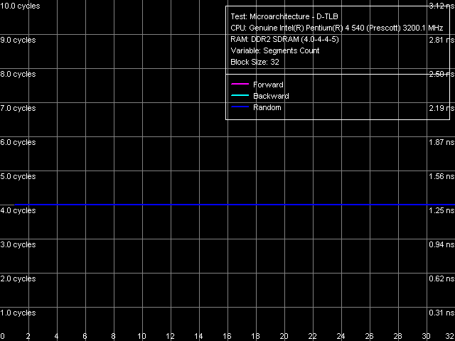 D-TLB associativity, Pentium EE 840
D-TLB size is 64 page entries (we have already seen that in the other test results), a miss penalty (when the TLB size is used up) costs a processor minimum 57 cycles. Associativity - full. 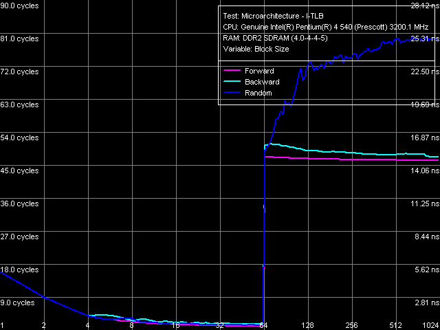 I-TLB size, Pentium EE 840 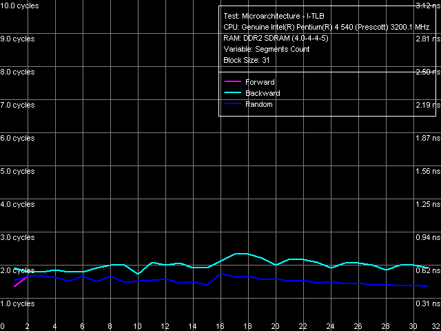 I-TLB associativity, Pentium EE 840 I-TLB size is 64 entries, the miss penalty is 45 cycles (forward, backward walk) and higher (random walk), full associativity. It's important to note that the buffer size (which is a shared resource) in this processor does not grow to 128 entries when Hyper-Threading is disabled (according to CPUID data as well as to the test results), which used to be demonstrated by all Pentium 4 processors. This behaviour is rather strange. At least it shouldn't be inevitable due to the dual core, considering that each core is like a separate, independent physical processor with its own resources like I-TLB. There is just a chance that the current first revision of Smithfield core had some problems, which didn't allow the full sized I-TLB with disabled Hyper-Threading, or this issue was just... forgotten by the manufacturer :). ConclusionOur analysis shows that the new Smithfield core can be considered a sterling successor to the NetBurst microarchitecture, implemented in Prescott, Nocona, and Irwindale cores. According to CPUID characteristics as well as the results of our today's tests, the new core (to be more exact, its single-core half) can be ranked somewhere between the latest revision of Nocona core (E0) and the latest revisions of Prescott/2M and Irwindale (N0) cores. Namely, the new Smithfield A0 core is characterized by absolutely the same construction of Trace Cache, decoder, pipeline, and execution modules, which is implemented in Prescott/2M and Irwindale cores. But due to a twice as small L2 Cache size (per one core) it has improved L1-L2 bus performance characteristics, which even surpass those of the Nocona E0 core.
Considering the above said as well as the organization of multi-core architecture (two independent, isolated cores, planted on the common system bus), we should expect that in terms of performance the new platform will be at least on a par with a dual-processor system with equally-clocked Intel Xeon processors on Nocona E0 cores, or even outperform it due to the improved memory controller, integrated into the Intel 955X chipset. Write a comment below. No registration needed!
|
Platform · Video · Multimedia · Mobile · Other || About us & Privacy policy · Twitter · Facebook Copyright © Byrds Research & Publishing, Ltd., 1997–2011. All rights reserved. | ||||||||||||||||||||||||||||||||||||||||||||||||||||||||||||||||||||||||||||||||||||||||||||||||||||||||||||||||||||||||||||||||||||||||||||||||||||||||||||||||||||||||||||||||||||||||||||||||||||||||||||||||||||||||||||||||||||||||||||||||||||||||||