|
||
|
||
| ||
|
||
|
||
| ||
Testbed Configurations and Software
Testbed ¹1
Testbed ¹2
Software
CPUID Characteristics
We'll start the analysis of the new Prescott core revision with selected characteristics generated by the CPUID instruction. Pentium 4 660
Among the most important distinctions, which distinguish the new Prescott core revision in the 600 series of Pentium 4 processors from the previous revision, one can note, first of all, the core stepping increase to 3 (the new cores have the 0F43h signature, the last E0 revision was characterized by the 0F41h signature). Taking into account that the manufacturer assigns a letter "of a higher rank" to the alpha-numeric designation of each next Prescott core revision without modifying the numeric index (revision C0 is followed by D0 and then E0), the new revision can presumably be referred to as F0, this designation will be used in this article. It'll be interesting to see whether it's actually true.
There is one noteworthy modification in the Cache/TLB descriptors, one of them is changed from 7Ch to 7Dh, which means an upgrade from 1MB to 2MB L2 Cache preserving its other characteristics (associativity and line size). Nevertheless, the most interesting characteristics in our opinion are those of the key features of the new core revision. Aside from the support for Thermal Monitor 2 and Execute Disable bit (they were already included into the E0 revision of Prescott core, i.e. "J series" of Pentium 4 processors), the new core revision supports Enhanced Intel SpeedStep and EM64T, which are natively supported by server Nocona cores. It's interesting to note two currently "unknown" (i.e. not available in the official documentation) technologies, denoted by Bits 2 and 13 of the ECX register. Perhaps they will be used to denote those LaGrande and VanderPool technologies, which are currently "hidden" from regular users. We hope it'll become clear with the new revision of the document Intel(R) Processor Identification and the CPUID Instruction, Application Note 485, its latest 027 revision is dated July 2004.
So, by all of the above-mentioned parameters the new revision of Prescott core can be actually considered a desktop incarnation of the latest E0 revision of the server Nocona core. Besides, it is equipped with two megabytes of L2 Cache. Let's proceed to the new extreme series of Pentium 4 processors. Pentium 4 Extreme Edition 3.73 GHz
Where does its "extremity" lie? The answer to this question is absolutely not obvious. This processor lacks the traditional component of an extreme series - L3 Data Cache. However, no one promised that the "extremity" lies in L3 Cache. Moreover, that's not unexpected, taking into account that there is absolutely no use in 2MB L3 Cache and inclusive organization of the Data Cache in the presence of 2MB L2 Cache! (in case of the inclusive cache organization, the efficient volume of the cached space is equal to the volume of the largest cache, but not to the total volume of all cache levels). It's quite possible that the "extremity" means the core capacity to operate at 266MHz of the FSB (which we didn't manage to obtain with our first sample under review), because... there are just no other options.
Let's go on: CPUID signature in this model is again 0F43h, i.e. it's sort of the same new F0 revision of Prescott core, implemented in the 600 series of Pentium 4 processors. Nevertheless, there are obvious differences in features between those seemingly identical cores. For example, the extreme version... lacks Thermal Monitor 2 and Enhanced Intel SpeedStep. Nevertheless, it offers XD bit and EM64T, as well as the two "unknown" technologies, which we already mentioned above.
Thus, by CPUID characteristics the first extreme series of Prescott cores is quite an ambiguous phenomenon. Part of its technologies was obviously borrowed from the previous E0 revision of the extreme Prescott core (XD bit), and another part - from the server Nocona core (EM64T). But the whole point is that only part of them - for some reason the new extreme core was "deprived" of TM2 (from Prescott E0) and Enhanced Intel SpeedStep (from Nocona), which are available in the same revision of the non-extreme Prescott core (see above). It seems that the reasons are clear only to the CPU manufacturer, but it obviously managed to confuse users very well...
Real Bandwidth of Data Cache/Memory
Let's proceed to the RMMA rest results for the new processors. The general picture of the real throughput of memory system levels (L1/L2/RAM) in Pentium 4 660 and Pentium 4 EE 3.73 looks the same. |
|||||||||||||||||||||||||||||||||||||||||||||||||||||||||||||||||||||||||||||||||||||||||||||||||||||||||||||||||||||||||||||||||||||||||||||||||||||||||||||||||||||||||||||||||||||||||||||||||||||||||||||||||||||||||||||||||||||||||||||||||||||||||||||||||||||||||||||||||||||||||||||||||||||||||||||||||||||||||||||||||
| Level | Average bandwidth, byte/cycle (MB/sec) | |||
| Pentium 4 (Prescott D0) |
Xeon (Nocona D0) |
Pentium 4 660 (Prescott F0) |
Pentium 4 EE (Prescott F0) |
|
| L1, reading, MMX L1, reading, SSE L1, writing, MMX L1, writing, SSE |
7.98 15.93 2.91 3.56 |
7.96 15.93 2.90 3.54 |
7.98 15.93 2.91 3.56 |
7.98 15.93 2.91 3.56 |
| L2, reading, MMX L2, reading, SSE L2, writing, MMX L2, writing, SSE |
4.41 8.02 2.91 3.56 |
4.39 7.84 2.89 3.54 |
4.53 8.13 2.91 3.56 |
4.57 8.20 2.91 3.56 |
| RAM, reading, MMX RAM, reading, SSE RAM, writing, MMX RAM, writing, SSE |
3901.4 MB/sec 4457.4 MB/sec 1750.0 MB/sec 1760.6 MB/sec |
3215.2 MB/sec 3620.1 MB/sec 1863.0 MB/sec 1855.0 MB/sec |
5187.3 MB/sec 5490.6 MB/sec 2061.8 MB/sec 2057.8 MB/sec |
6002.8 MB/sec 6540.3 MB/sec 2216.9 MB/sec 2218.1 MB/sec |
The quantitative characteristics of L1 Cache bandwidth are unchanged - they match those for previous Prescott and Nocona cores, D0 revision. L2 Cache bandwidth characteristics are somewhat different - in particular, you can see a tad higher read efficiency of this cache level in both processors (average L2 Cache bandwidth within the 20 - 240KB range). Nevertheless, considering the substantial spread of this value within the specified range, it can hardly be considered a symptom of a thorough core revision - it's rather just a measurement error :).
Nevertheless, memory bandwidth values demonstrate noticeable changes - the real read bandwidth of this memory system level is noticeably higher. On the one hand, this may be due to the further improvement of the hardware prefetch algorithm, on the other hand - a consequence of using the new i925XE chipset, where the manufacturer probably managed a more efficient memory controller. Higher memory bandwidth values on Pentium 4 EE 3.73 can be explained by the 266MHz FSB frequency (which increases its peak bandwidth up to 8.53GB/sec) and the memory operating in FSB-synchronous mode (FSB:DRAM frequency ratio - 1:1).
As usual (for Pentium 4 processors), Software Prefetch method allows
maximum memory bandwidth, while other methods are not so highly efficient.
Real memory bandwidth to software prefetch distance curves for Pentium 4 660 and Pentium 4 EE 3.73 match on the qualitative level - only quantitative indices are different, they are connected with different FSB frequencies (200MHz in Pentium 4 660 versus 266MHz in Pentium 4 EE 3.73). The obtained prefetch curves are typical of Prescott cores (in outward appearance they match with those we obtained for the previous revisions of this core). Besides, they indicate the lack of differences in software prefetch algorithms in non-extreme and extreme modifications of the new Prescott core F0 revision.
| Access mode | Maximum memory read bandwidth, MB/sec* | |||
| Pentium 4 (Prescott D0) |
Xeon (Nocona D0) |
Pentium 4 660 (Prescott F0) |
Pentium 4 EE (Prescott F0) |
|
| reading, MMX reading, SSE reading, MMX, SW Prefetch reading, SSE, SW Prefetch reading, MMX, Block Prefetch 1 reading, SSE, Block Prefetch 1 reading, MMX, Block Prefetch 2 reading, SSE, Block Prefetch 2 Reading cache lines, forward Reading cache lines, backward |
3901.4 (61.0%) 4457.4 (69.6%) 6311.3 (98.6%) 6334.2 (99.0%) 4191.0 (65.5%) 4614.8 (72.1%) 3948.3 (61.7%) 4517.2 (70.6%) 5180.9 (81.0%) 5178.7 (80.9%) |
3215.2 (50.2%) 3620.1 (56.6%) 5334.2 (83.3%) 5329.9 (83.3%) 3302.2 (51.6%) 3524.3 (55.1%) 3392.3 (53.0%) 3784.5 (59.1%) 3313.5 (51.8%) 3315.8 (51.8%) |
5187.3 (81.1%) 5490.6 (85.8%) 4630.6 (72.4%) 5046.4 (78.9%) 5146.9 (80.4%) 5492.2 (85.8%) 5968.8 (93.3%) 5957.7 (93.1%) |
6002.8 (70.3%) 6540.3 (76.6%) 8314.7 (97.4%) 8508.5 (99.7%) 5490.0 (64.3%) 6069.2 (71.1%) 5936.4 (69.6%) 6557.0 (76.8%) 7623.3 (89.3%) 7613.2 (89.2%) |
Quantitative indices demonstrate that Software Prefetch is
of more "help" to Pentium 4 EE 3.73 (its usage advantage on
this platform is higher) than to Pentium 4 660. The reason for
this phenomenon is quite evident - software prefetch efficiency
is actually the same in both processors, but Pentium 4 660 reaches
the theoretical maximum FSB bandwidth faster than Pentium 4
EE 3.73. Nevertheless, both processors reach nearly maximum
efficiency of reading data from memory (100% and even higher
:)) in the area of Software Prefetch maximum efficiency - at
prefetching data, which is 768-1024bytes away from the requested
data. |
| Access mode | Maximum memory write bandwidth, MB/sec* | |||
| Pentium 4(Prescott D0) | Xeon(Nocona D0) | Pentium 4 660(Prescott F0) | Pentium 4 EE(Prescott F0) | |
|
Writing, MMX |
1750.0 (27.3%) 1760.6 (27.5%) 4265.9 (66.7%) 4266.0 (66.7%) 2283.9 (35.7%) 2254.2 (35.2%) |
1855.0 (29.0%) 4236.2 (66.2%) 4235.9 (66.2%) 2380.2 (37.2%) 2386.1 (37.3%) |
2061.8 (32.2%) 2057.8 (32.2%) 4255.0 (66.5%) 4254.9 (66.5%) 2527.7 (39.5%) 2435.0 (38.0%) |
2216.9 (26.0%) 2218.1 (26.0%) 5704.7 (66.9%) 5706.7 (66.9%) 2759.7 (32.3%) 2702.9 (31.7%) |
*values in parentheses are given relative to the theoretical maximum of memory bandwidth (6.4GB/sec for 200MHz FSB, 8.53GB/sec for 266MHz FSB)
What concerns maximum real memory write bandwidth, you can see that little has changed here - the use of forward write method allows to reach 2/3 of maximum theoretical FSB throughput in all cases. Efficiency of writing cache lines can also be considered practically the same in all cases: gains relative to the average memory write bandwidth amount for approximately 500MB/sec.
The overall picture of latency, as well as of memory bandwidth,
in both processors looks the same.
Typical features of Data Cache and D-TLB organization are no less clear in this test: 16KB and 2MB inflections, which correspond to L1 and L2 Cache sizes, as well as smooth rise of random access latency in L2 Cache with the block size starting from 256KB.
| Level, access | Average latency, cycles (ns) | |||
| Pentium 4(Prescott D0) | Xeon(Nocona D0) | Pentium 4 660(Prescott F0)** | Pentium 4 EE(Prescott F0)** | |
| L1 |
|
|
|
|
| L2 |
|
|
|
|
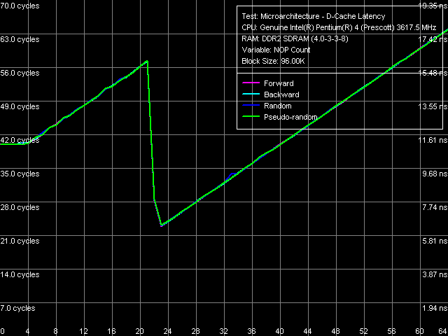
| RAM, forward RAM, backward RAM, random* RAM, pseudo random* |
41.1 hc 126.0 hc 56.1 hc |
52.6 hc 134.1 hc 75.8 hc |
36.8 hc (77.2 hc) 106.1 hc (111.0 hc) 52.0 hc (80.4 hc) |
33.9 hc (73.8 hc) 101.4 hc (106.2 hc) 49.4 hc (76.6 hc) |
*4MB block size
**Values in parentheses are obtained with disabled Hardware Prefetch
Quantitative latency characteristics of L1 and L2 Cache are the same for all processors included into the table. By the way, 4-cycle L1 latency in Pentium 4 EE 3.73 can be considered the first experimental verification of the fact, that this processor is really based on Prescott core (as is well known, all previous Pentium 4 Extreme Edition processors were based on Gallatin core, its L1 Cache latency was 2 cycles).
Concerning the memory latency, the table values have been obtained in a separate test, where the data chain is walked at 128byte steps, i.e. the effective L2 Cache line size. Besides, for the first time we have published data obtained with disabled Hardware Prefetch for the new processors. This data illustrates its efficiency (the latest method for measuring memory latency on Pentium 4 platform is described in detail in our recent article "Two methods for measuring memory latency on Intel Pentium 4 platform in RightMark Memory Analyzer - how to choose the right one?").
Thus, memory latency in all walk modes decreased a little in comparison with the previously tested Pentium 4 platform (Prescott D0) - the latency drop is the most noticeable at random walk (about 20ns), obviously due to the new i925XE chipset (because Hardware Prefetch at random walk is practically idle, as we have already told above and will see below). Note also that memory latency in Pentium 4 EE 3.73 is a tad lower - the most obvious explanation is in synchronous memory operation on this platform.
In both cases disabled Hardware Prefetch results in almost 2.5-fold latency increase of forward and backward walk, it's a tad lower (approximately by 1.5 times) in case of pseudo random walk and is practically imperceptible at random walk. The results obtained can be considered a direct evaluation of Hardware Prefetch at various memory access modes - it reaches maximum in case of forward and backward walks, a tad lower for pseudo random walk (as we have assumed, in this case prefetch operates on the level of whole memory pages); and finally, this algorithm is practically idle at random walk. Unfortunately, it's currently impossible to compare the results of hardware prefetch efficiency obtained on new Prescott core revision with the previous revisions - measuring memory latency without hardware prefetch is a new developing tendency in our research. From the quantitative positions, the "true" average latency of Corsair DDR2-533 modules (used in our tests) is 80.4ns in asynchronous mode and 76.6ns in synchronous mode. Lower latencies in backward walk mode with disabled Hardware Prefetch are an interesting but unexplainable fact.

L1-L2 bus unload curves, i.e. minimum L2 latency, look the same for both processors and are quite typical of Prescott cores: latency of this level obviously does not reach its maximum at standard L1-L2 bus "unloading" by inserting "empty" operations (Method 1), and it goes down to 22 cycles at "non-standard" unloading, specially developed for processors with pronounced speculative data loading (Method 2).
"Standard" L2-RAM bus unloading curves for both processors are no
different from the ones we previously obtained on Prescott and Nocona
cores, D0 revision.
| Level, access | Minimum latency, cycles (ns) | |||
| Pentium 4(Prescott D0) | Xeon(Nocona D0) | Pentium 4 660(Prescott F0) | Pentium 4 EE(Prescott F0) | |
| L1 |
|
|
|
|
| L2* |
|
|
|
|
|
RAM**, forward |
31.1 hc 125.2 hc 55.0 hc |
41.2 hc 134.0 hc 74.5 hc |
31.1 hc (77.9 hc) 105.4 hc (109.9 hc) 50.9 hc (79.4 hc) |
27.6 hc (74.1 hc) 100.6 hc (105.3 hc) 48.5 hc (75.9 hc) |
*Values in parentheses are obtained by Method 2
**Values in parentheses are obtained with disabled Hardware Prefetch
***4MB block size
We should again note the decrease of memory access latency (in comparison with the previously reviewed Pentium 4 platform), which is practically imperceptible at forward and backward walks and maximum (20-25ns) at random walk. Note that minimum memory access latency values are practically no different from the average values obtained in the previous test, except for the forward and backward walk modes, where hardware prefetch gets an additional advantage from unloading L2-RAM bus (BIU). This assertion certainly does not extend to measurements with disabled Hardware Prefetch.
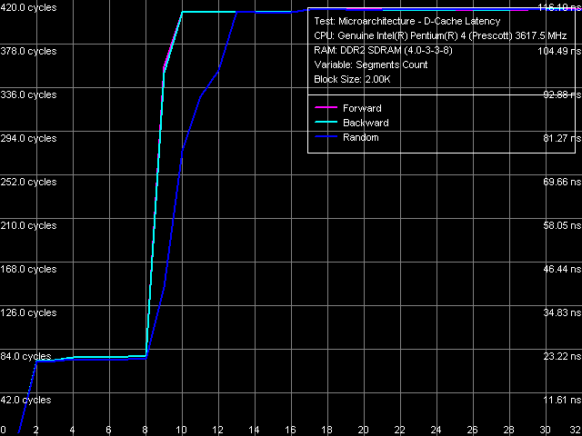
L1/L2 D-Cache associativity test for both processors, which result is shown on the picture, indicates the lack of any changes in this parameter. As in all the other reviewed Pentium 4/Xeon processors, the "effective" L1 data cache associativity is equal to 1, associativity of the integrated L2 instruction cache/data cache - 8.
| Access mode | Bandwidth, bytes/cycle* | |||
| Pentium 4 (Prescott D0) | Xeon (Nocona D0) | Pentium 4 660 (Prescott F0) | Pentium 4 EE (Prescott F0) | |
|
Reading (forward) |
16.40 (51.3%) 4.76 (14.9%) 4.75 (14.9%) |
16.42 (51.3%) 4.79 (15.0%) 4.78 (14.9%) |
14.53 (45.4%) 3.99 (12.5%) 4.00 (12.5%) |
14.60 (45.6%) 4.10 (12.8%) 4.10 (12.8%) |
*values relative to theoretical limit are in parentheses
Though the above quantitative characteristics (bandwidth, latency) of L1 and L2 D-Caches in the processors under review almost match the test results of previous Prescott and Nocona core revisions, the present test results open up new unexpected details on the L1-L2 bus design. Namely, you cannot fail to notice the further decrease of its efficiency to 45.3-45.8% for reading operations and up to 12.5-12.8% for writing operations (in good old times - i.e. Northwood core period, the efficiency of this bus utilization in reading operations used to be close to the theoretical maximum).
Let's examine another interesting component of the NetBurst microarchitecture
- its specialized cache for micro-operations (Execution Trace Cache)
provided by the predecoder. Assumptions about its size being increased
to 16000 micro-operations and the introduction of quadruple prefetch
of micro-operations per cycle (which started to circulate when server
Nocona cores appeared) proved to be wrong again.

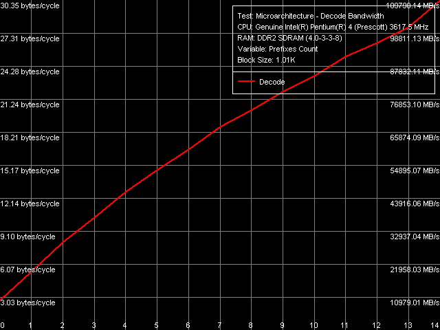
As always, the overall picture of decode/execute speed for "large" 6-byte CMP instructions is the most illustrative. In this test, as in all the other tests of this type, there are no qualitative changes in behaviour of Prescott cores under review. Let's proceed to the quantitative evaluation.
| Instruction type | Effective size of Trace Cache, KB (Kuop) | Decode efficiency, bytes/cycle (instructions/cycle) | |
| Trace Cache | L2 Cache | ||
| Independent | |||
| NOP |
|
|
|
| SUB |
|
|
|
| XOR |
|
|
|
| TEST |
|
|
|
| XOR/ADD |
|
|
|
| CMP 1 |
|
|
|
| CMP 2 |
|
|
|
| CMP 3 |
|
|
|
| CMP 4 |
|
|
|
| CMP 5 |
|
|
|
| CMP 6* |
|
|
|
| Prefixed CMP 1 |
|
|
|
| Prefixed CMP 2 |
|
|
|
| Prefixed CMP 3 |
|
|
|
| Prefixed CMP 4* |
|
|
|
| Dependent | |||
| LEA |
|
|
|
| MOV |
|
|
|
| ADD |
|
|
|
| OR |
|
|
|
| SHL |
|
|
|
| ROL |
|
|
|
*2 micro-operations
**in the assumption that prefixes are truncated before they are placed into Trace Cache
To track the general tendency of changes, let's provide the data obtained for Xeon (Nocona core, D0 revision) for a control point. This processor core, equipped with EM64T, was the first to show the deterioration tendency for decode/execute efficiency of some commands - in particular, simple operations like TEST (test eax, eax) and CMP 1 (cmp eax, eax). Let's see what changes this micro-architectural component suffered in the new Prescott core revision, which also supports EM64T.
| Instruction type | Effective size of Trace Cache, KB (Kuop) | Decode efficiency, bytes/cycle (instructions/cycle) | |
| Trace Cache | L2 Cache | ||
| Independent | |||
| NOP SUB XOR TEST XOR/ADD CMP 1 CMP 2 CMP 3 CMP 4 CMP 5 CMP 6* Prefixed CMP 1 Prefixed CMP 2 Prefixed CMP 3 Prefixed CMP 4* |
22.0 (11.0) 22.0 (11.0) 22.0 (11.0) 22.0 (11.0) 22.0 (11.0) 44.0 (11.0) 63.0 (10.5) 63.0 (10.5) 63.0 (10.5) 32.0 (10.6) 63.0 (7.9; 10.5**) 63.0 (7.9; 10.5**) 63.0 (7.9; 10.5**) 44.0 (11.0; 14.7**) |
5.73 (2.87) 3.99 (2.00) 3.42 (1.71) 5.73 (2.87) 5.16 (2.58) 10.32 (2.58) 15.48 (2.58) 15.48 (2.58) 15.48 (2.58) 8.67 (1.45) 20.62 (2.58) 20.60 (2.58) 20.60 (2.58) 11.56 (1.45) |
2.00 (1.00) 2.00 (1.00) 2.00 (1.00) 2.00 (1.00) 2.00 (1.00) 3.99 (1.00) 4.00 (0.67) 4.00 (0.67) 4.00 (0.67) 4.00 (0.67) 4.14 (0.52) 4.14 (0.52) 4.14 (0.52) 4.14 (0.52) |
| Dependent | |||
| LEA MOV ADD OR SHL ROL |
- - - - - |
2.01 (1.00) 2.01 (1.00) 2.00 (1.00) 3.00 (1.00) 3.00 (1.00) |
2.01 (1.00) 2.01 (1.00) 2.00 (1.00) 3.00 (1.00) 3.00 (1.00) |
*2 micro-operations
**in the assumption that prefixes are truncated before they are placed into Trace Cache
Differences between these two processors are so insignificant, that we decided to publish the "mean" data in a single table. Alas, the CPU performance deterioration tendency (execution of some commands) is also active here - i.e. EM64T introduction costs dear. First of all, you can see the increasingly less efficient execution of TEST and CMP 1 - the execution speed of the former dropped to 1.71 instructions/cycle, of the latter - to 2.58 instructions/cycle. One can say that the latter dropped to the execution efficiency level of other CMP commands (2-5). The second significant modification, which again represents the new core revision in an unfavourable light, is the reduction of maximum decode/execute speed for all CMP operations from L2 Cache to 4.0 bytes/cycle (1.0 or 0.67 instructions/cycle, depending of the command size) as well as "prefix" CMP to 4.14 bytes/cycle (0.52 instructions/cycle).
The second significant efficiency deterioration of the decoder/pipeline
in Nocona core with EM64T was in the decreased efficiency of truncating
"meaningless" prefixes in the test that executed instructions of the
type [0x66]nNOP, n = 0..14.
| Number of prefixes | Decode/execute efficiency,bytes/cycle (instructions/cycle) | |||
| Pentium 4(Prescott D0) | Xeon(Nocona D0) | Pentium 4 660(Prescott F0) | Pentium 4 EE(Prescott F0) | |
| 0 1 2 3 4 5 6 7 8 9 10 11 12 13 14 |
5.68 (2.84) 8.52 (2.84) 11.34 (2.84) 14.09 (2.82) 16.89 (2.82) 19.51 (2.79) 22.30 (2.79) 24.87 (2.76) 27.54 (2.75) 30.76 (2.80) 33.24 (2.77) 35.86 (2.76) 38.18 (2.73) 40.85 (2.72) |
5.41 (2.71) 8.16 (2.72) 10.48 (2.62) 12.73 (2.55) 14.73 (2.46) 16.63 (2.38) 18.75 (2.34) 20.63 (2.29) 21.93 (2.19) 23.44 (2.13) 25.78 (2.15) 27.14 (2.09) 28.64 (2.05) 30.33 (2.02) |
5.43 (2.72) 8.13 (2.71) 10.42 (2.61) 12.74 (2.55) 14.74 (2.46) 16.64 (2.38) 18.76 (2.35) 20.23 (2.25) 21.96 (2.20) 23.45 (2.13) 25.17 (2.10) 26.46 (2.04) 27.89 (1.99) 30.35 (2.02) |
5.43 (2.72) 8.13 (2.71) 10.42 (2.61) 12.74 (2.55) 14.74 (2.46) 16.64 (2.38) 18.76 (2.35) 20.23 (2.25) 21.96 (2.20) 23.45 (2.13) 25.17 (2.10) 26.46 (2.04) 27.89 (1.99) 30.35 (2.02) |
The new revision of Prescott cores with EM64T is no different in this respect, or the difference is insignificant: decreased execution speed of "prefix" NOPs with the increased number of prefixes in new Prescott processors almost coincides with the Nocona core (except for one additional, easily reproduced "slump" in case of 13 prefixes before the NOP instruction). Thus, the conclusion previously drawn about the first "64-bit" Nocona core also extends to the new "64-bit" revision of Prescott core: truncating extra prefixes, which is the function of the x86-instruction decoder located before Trace Cache, is less effective now. It's quite logical to assume that this concerns not only prefixes but the operation efficiency of the decoder on the whole.
We shall not go into the analysis of D-TLB and I-TLB characteristics,
considering that they (by CPUID descriptors) match in all processors
under review.
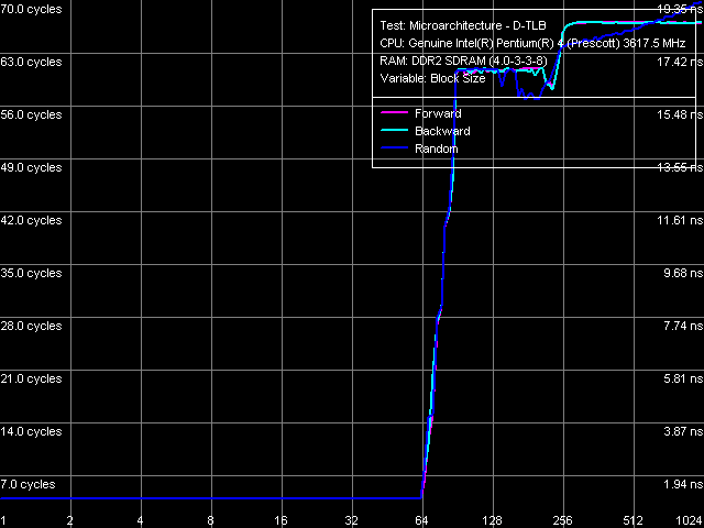
D-TLB size is 64 page entries (we have already seen that in the other
test results), a miss penalty (when the TLB size is used up) costs
a processor minimum 57 cycles. Associativity - full.
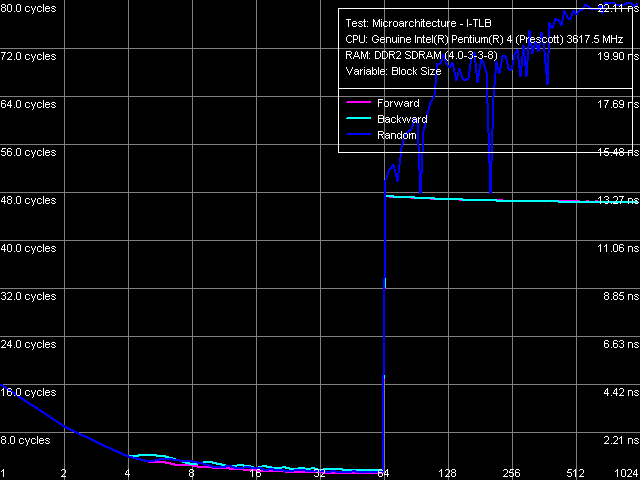

I-TLB size is 64 entries (this resource is divided in two between logical processors when Hyper-Threading is enabled), a miss penalty is 45 cycles (forward, backward walks) and more (random walk), associativity - full.
In our previous analysis of the NetBurst microarchitecture we marked one interesting but not so sunny - both to the manufacturer and to end users - tendency of this microarchitecture in every next implementation. This tendency lies in... gradual deterioration of low-level characteristics of the microarchitecture under review as it develops, i.e. introducing the increasing number of "bells and whistles". Remember, when we upgraded from Northwood to Prescott, together with SSE3 we "inherited" a significantly increased D-Cache latencies, noticeable reduction of the effective bandwidth of the L1-L2 bus, and finally decreased code execution efficiency. And the upgrade to the server modification of Prescott - the first x86-64-compatible Nocona core - resulted in a further execution speed reduction of some commands and the decreased decoder efficiency in general.
Alas, the conclusion that can be drawn by our today's test results will be very pessimistic: the above tendency... goes on. The new "64-bit" revision of Prescott core is characterized by further reduction of L1-L2 D-Cache bus throughput and of the execution speed of comparison operations.
What concerns the comparison of non-extreme and extreme versions of the new Prescott core revision, our tests demonstrate that their microarchitectures are completely identical. Thus, the same CPUID signature (0F43h) in both processors, despite some different features, is partially justified - this is indeed the same core. But in the first case (600 series Pentium 4) it operates with 200MHz FSB, and it features (even "boasts of") TM2 and EIST technologies. And in the second case (Pentium 4 Extreme Edition 3.73GHz - this processor hasn't got its number yet) the core can operate with 266MHz FSB. TM2 and EIST technologies, which are certainly implemented in this core, are hidden well on the hardware level.
Note that Pentium 4 Extreme Edition 3.73GHz is the first case (certainly, not an only one in future), when the CPU "extremity" is set by an increased FSB frequency instead of a large L3 D-Cache. But in such a case the "extremity" notion gets more than conventional - one can always try to find a better sample (than in our case) of the "non-extreme" Pentium 4 processor of the 600 series and make it work with 266MHz FSB. In conclusion we want to note that such an approach to "extremity" may also indicate revocation of design and/or production of Potomac core (a counterpart of Prescott core with L3 D-Cache) - at least in the desktop sector (leaving the ground only to the server modifications with very large L3 Cache, which significantly surpasses the current 2MB L2 Cache size).
Write a comment below. No registration needed!
|
Article navigation: |
| blog comments powered by Disqus |
| Most Popular Reviews | More RSS |
 |
Comparing old, cheap solutions from AMD with new, budget offerings from Intel.
February 1, 2013 · Processor Roundups |
 |
Inno3D GeForce GTX 670 iChill, Inno3D GeForce GTX 660 Ti Graphics Cards A couple of mid-range adapters with original cooling systems.
January 30, 2013 · Video cards: NVIDIA GPUs |
 |
Creative Sound Blaster X-Fi Surround 5.1 An external X-Fi solution in tests.
September 9, 2008 · Sound Cards |
 |
The first worthwhile Piledriver CPU.
September 11, 2012 · Processors: AMD |
 |
Consumed Power, Energy Consumption: Ivy Bridge vs. Sandy Bridge Trying out the new method.
September 18, 2012 · Processors: Intel |
| Latest Reviews | More RSS |
 |
Retested all graphics cards with the new drivers.
Oct 18, 2013 · 3Digests
|
|
Added new benchmarks: BioShock Infinite and Metro: Last Light.
Sep 06, 2013 · 3Digests
|
|
Added the test results of NVIDIA GeForce GTX 760 and AMD Radeon HD 7730.
Aug 05, 2013 · 3Digests
|
 |
Gainward GeForce GTX 650 Ti BOOST 2GB Golden Sample Graphics Card An excellent hybrid of GeForce GTX 650 Ti and GeForce GTX 660.
Jun 24, 2013 · Video cards: NVIDIA GPUs
|
|
Added the test results of NVIDIA GeForce GTX 770/780.
Jun 03, 2013 · 3Digests
|
| Latest News | More RSS |
Platform · Video · Multimedia · Mobile · Other || About us & Privacy policy · Twitter · Facebook
Copyright © Byrds Research & Publishing, Ltd., 1997–2011. All rights reserved.