Sony Develops Back-illuminated CMOS Sensor
Sony Corporation announced the development of a back-illuminated CMOS image sensor (pixel size: 1.75µm square pixels, five effective mega pixels, 60 frames/s) with significantly enhanced imaging characteristics, including nearly twofold sensitivity and low noise. This improved performance has been achieved by illuminating the backside of the silicon substrate, in contrast to conventional CMOS image sensors based on front-illumination technology.
The newly developed CMOS image sensor achieves a signal-to-noise ratio of +8dB (+6dB sensitivity, -2dB noise) in comparison to existing Sony CMOS image sensors of the same pixel size. Sony will apply this back-illuminated CMOS technology in consumer digital video camcorders and digital still cameras to deliver an even higher quality image experience.
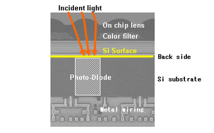
With a conventional front-illumination structure, the metal wiring and transistors on the surface of the silicon substrate that form the sensor's light-sensitive area (photo-diode) impede photon gathering carried out by the on-chip lens, and this has also been an important issue in the miniaturization of pixels and widening optical angle response.
A back-illuminated structure minimizes the degradation of sensitivity to optical angle response, while also increasing the amount of light that enters each pixel due to the lack of obstacles such as metal wiring and transistors that have been moved to the reverse of the silicon substrate.
However, compared to conventional front-illuminated structures, back-illuminated structures commonly causes problems such as noise, dark current, defective pixels and color mixture that lead to image degradation and also cause a decrease in the signal-to-noise ratio.
To overcome this Sony has newly developed a unique photo-diode structure and on-chip lens optimized for back-illuminated structures, that achieves a higher sensitivity of +6dB and a lower random noise of -2dB without light by reducing noise, dark current and defect pixels compared to the conventional front-illuminated structure. Additionally, Sony's advanced technologies such as high-precision alignment have addressed any color mixture problems.
Furthermore, the back-illuminated structure also expands device potential in areas such as speed and dynamic range by enabling multiple metal wiring layers and greater flexibility in the transistor structure.
Source: Sony Corporation
Write a comment below. No registration needed!