Samsung Develops 16-Chip Multi-Stack Package Technology
Samsung Electronics Co., Ltd. announced that it has developed the industry's first process to enable production of a 16-chip multi-chip package of memory. The new MCP technology supports the industry-wide demand for small form factors and high-densities that will accommodate multimedia-intensive user applications. Samsung's new 16-chip MCP technology, when applied to 8Gb NAND flash chips, can enable up to a 16 gigabyte MCP solution.
Advanced multi-chip package technology requires a combination of key processes such as wafer thinning technology, redistribution layer technology, chip sawing technology and wire bonding technology.
To increase the number of chips stacked vertically, the need for further wafer thinning was a critical design obstacle. For the new 16-chip process, Samsung introduced wafer-thinning technology that eliminates 24 over 25 (24/25) of the thickness of each fabricated-wafer to reduce the overall thickness to only 30-micrometers. This is 65% the thickness of the 10-chip MCP wafer (45µm) Samsung developed in 2005 and similar to the size a human cell, which measures 20 to 30 µm.
Samsung also developed a new laser-cutting technology to cut the wafer into individual chips. This new cutting process prevents the memory chips from breaking into pieces when they are cut using conventional blade sawing technology, which was originally designed only for sawing wafers up to 80µm-thick.
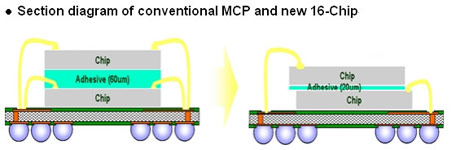
To vertically stack identically-sized dies (chips), a redistribution layer technology also is applied in Samsung's new multi-stack MCP process, to enable wafer fabricators to adhere the wire contacts from just one side, unlike the conventional method of extending wire connection from both sides of each chip. Along with a single wire contact per die, the dies are placed in a zig-zag stack to minimize the use of space and the length of the wire connectors. Moreover, the thickness of the adhesive has been reduced to 20µm bringing the height of a 16-die stacked height to 1.4mm. (A 10-chip MCP uses 60µm adhesive layer and has a total height of 1.6mm.)
Source: Samsung Electronics Co., Ltd.
Write a comment below. No registration needed!