NVIDIA GeForce FX5700LE: the first photos and specs
The latest WHQL-certified NVIDIA ForceWare 56.55 driver disturbed the Web with the following strings in it:
- NVIDIA_NV34DEV_0326.1 = "NVIDIA GeForce FX 5500
- NVIDIA_NV36DEV_0343.1 = "NVIDIA GeForce FX 5700LE
- NVIDIA_NV36DEV_0344.1 = "NVIDIA GeForce FX 5700VE
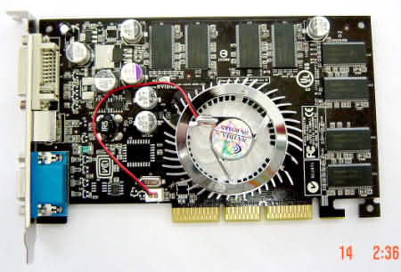
Speaking of GeForce FX 5500 specs and features, we will offer you the new material in the nearest future, when we have enough trustworthy information. Pity, but we still have no reliable facts on GeForce FX 5700VE, however, our colleagues from Chinese GZeasy not only provided us with the GeForce FX 5700LE specs, but also shared with us the first photos of a card on this GPU.
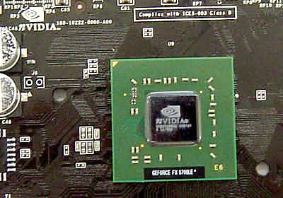
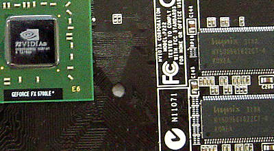
Judging by FC-PGA package of GeForce FX 5700LE GPU, we suppose it will be selected from 0.13µm NV36 scrappage. Similar to the more powerful 5700/5700 Ultra, it features CineFX 2.0 engine, supports IntelliSample, HCT, and UltraShadow, however its clock rate is reduced to 250MHz (vs. 425MHz of a standard GeForce FX 5700).
The GeForce FX 5700LE-based card shown on the photo, has 4-layer P222 PCB designed totally different from P191 boards of GeForce FX 5700 and P141 boards of GeForce FX 5600. The card on GeForce FX 5700LE has eight Hynix´s 4ns DDR memory chips, i.e. 128MB of 128-bit memory.
Well, such an off-season, when the previous chip is "mastered" (though can´t say GF FX 5700 Ultra is available in volumes now), and the new one exists only in roadmaps, is the best time to release inexpensive GPUs with reduced clock rates. It seems that 5700LE-based solutions operating at 250/400MHz will soon compete with the previous "LE" solutions, GeForce FX 5600XT cards clocked at 235/400MHz.
Source: GZeasy
Write a comment below. No registration needed!


