 |
||
|
||
| ||
The RV790, RADEON HD 4800 series
RADEON HD 4890 specifications
Minor modifications of the chip described below helped AMD roll out a faster solution, ranking above the old RADEON HD 4870. HD 4890 differs from them in improved speed characteristics and much lower idle power consumption. However, it's the effect of much lower operating frequencies in 2D mode (versus RV770) rather than the new GPU. Unlike previous 4800-series solutions, there are no 512-MB modifications of HD 4890 anymore. The only model is equipped with 1 GB of video memory, which is the optimal memory size for Upper Mid-End graphics cards now. So 512 MB will be insufficient in some cases, while 1 GB will be for a long time. The new model has been given a logical name. It's a tad faster than HD 4870, so it's called HD 4890. This model number is crystal clear to users. It indicates that the card is faster, but belongs to the same family. Architecture and featuresFrom the architectural point of view, RV790 does not differ from RV770. It's just overhauled to achieve higher clock rates. What concerns technical characteristics, the first thing that catches the eye is the number of transistors increased to three millions and much larger surface area of RV790 versus RV770. The RV770 did not need many modifications, as it was already very good, well balanced and all that. It made no sense to increase the number of execution units without switching to the 40nm fabrication process (not ready for complex GPUs yet) because of the dual-GPU strategy for the High-End segment. So it was decided to make the GPU work at higher frequencies. Engineers overhauled the structure of RV770, changing its inner circuits and outputs. Besides, they added a so-called decap ring along the perimeter of the GPU, consisting of filtering (blocking) capacitors to help separate signals by reducing crosstalk. These changes led to a small increase in the number of transistors and enlarged the surface area of the chip.  As a result, RV790 really works better at higher frequencies than RV770, aided by slightly increased voltage. Its reference clock rate is higher by 100 MHz, and partners are now allowed to manufacture overclocked models operating at 900 MHz or higher. With any luck, overclockers can make them run at 1 GHz. But not all cards will overclock to this level without changing the cooling system, raising voltage, etc. The RV740, RADEON HD 4700 series
RADEON HD 4770 specifications
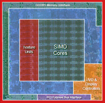
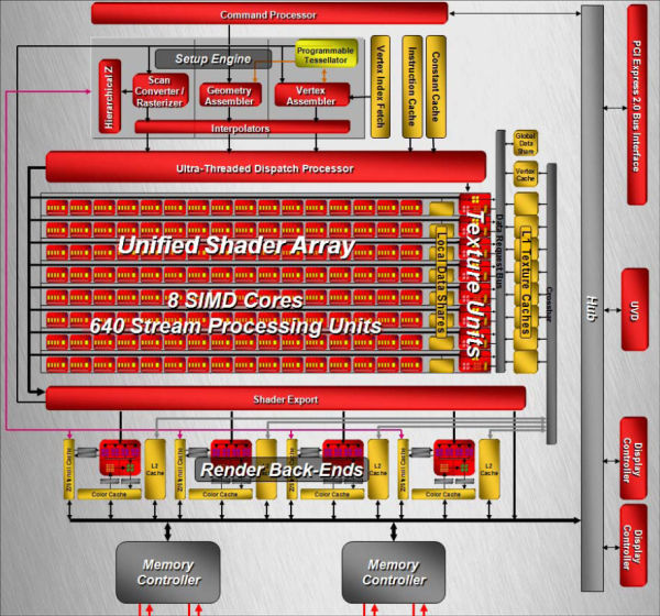
RADEON HD 4770 is the fastest solution among graphics cards for $100. A slower and cheaper card will be launched later -- HD 4750. RADEON HD 4770 has come to replace HD 4830, based on the RV770, which is inexpedient to manufacture, if it sells for $100. It's the new 40nm fabrication process that allowed AMD to offer an inexpensive robust solution with better characteristics than the old RADEON HD 4830. The new graphics card is faster and consumes much less power than the old product owing to the new 40nm fabrication process of its GPU and GDDR5 memory. It's only logical to equip HD 4770 with 512 MB of memory. Although new solutions can benefit from 1GB of video memory already, it's not expedient to install so much GDDR5 memory into a graphics card from this price range. Memory size of 512 MB is still an optimal choice for such graphics cards, which usually don't use high antialiasing levels. Architecture and featuresThe key theoretical features of the new architecture from AMD haven't changed, you can read about them in our baseline article about RV770. The Low-End GPU differs from RV770 only quantitatively, with several peculiarities, which we'll describe here. We already know that the R7xx architecture scales well, and the RV740 proves it once again:  So, RV740 differs from RV770/RV790 in the number of ALUs and TMUs. Besides, it has half as many 64-bit memory controllers. The new GPU copies the structure of RV770, to be more exact RV770LE, which is used in RADEON HD 4830. It has a part of its execution units disabled. The key quantitative changes: the number of shader processors in RV740 is reduced to 640 ALUs and 32 TMUs. But this time the company did not cut down ROPs. Consequences of the upgrade to the new fabrication process and a price drop for such a powerful solution include transition from the 256-bit bus to the 128-bit one. Surface of the 40nm die is much smaller than that of the 55nm die, so it's impossible to fit a 256-bit bus on the RV740. Besides, the 128-bit bus contributes to reduction of PCB manufacturing costs. But how can we avoid losing video memory bandwidth, it's so important for modern applications, especially ones using full-screen antialiasing and active post processing? AMD has an answer to this question! It's GDDR5 memory. The company has been using it since mid 2008 in RADEON HD 4870. GDDR5 memory provides twice as high bandwidth than GDDR3, so the HD 4770 hasn't lost much in memory bandwidth relative to the HD 4830. For example, GDDR5 memory used in the HD 4770 provides the effective frequency of 3200 MHz, while its physical frequency is only 800 MHz. As a result, memory bandwidth of RADEON HD 4770 exceeds 51 GB/s, while it's just a tad higher in the 256-bit HD 4830 with GDDR3 memory -- about 58 GB/s. Even though GDDR5 chips are more expensive than GDDR3, especially at the initial stages, a narrow memory bus allows to simplify PCB design and get an advantage, so it's the right decision in the long run. Besides, RADEON HD 4770 uses the second generation of GDDR5 memory powered by 1.5 V. It consumes less power than prev-gen memory chips. RV740 has an important advantage over RV770LE -- its GPU clock rate. HD 4770 operates at 750 MHz, so its theoretical performance values (arithmetic and texturing speed) exceed those of the HD 4830 by 30%. That is, close to the HD 4850. But that's not all as far as advantages of the new solution over RADEON HD 4830 are concerned. Despite the cut down memory bus, RV740 still contains 16 ROPs grouped by four. Interestingly, each of such Render Back-Ends (RBE) used to be accompanied by one 64-bit memory controller. But now, even though the GPU has four RBEs, the number of memory controllers has decreased to two (you can see it on the GPU diagram). What does it give us? Theoretical peak fillrate equal to that of the HD 4870. That is, higher than in the HD 4830 and even HD 4850. Considering that some of real applications are sometimes limited by the speed of ROPs, we can expect this card to be faster than the HD 4850 in several games. The 40nm process technologyThe 40nm fabrication process is expedient for GPU manufacturers. It produces much smaller GPUs and promises price drops in future. Transistor density provided by the 40nm fabrication process is much higher than that for the 55nm process. Theoretically, a 40nm chip will be smaller by 40% than the same chip manufactured by the 55nm fabrication process. For example, RV740 is about 140 square millimeters, much smaller than the 55nm RV770 (260 sq. mm). Fewer execution units in this GPU also have to do with it, of course. But the new fabrication process has a much stronger effect. What concerns manufacturing costs, they will drop only in future, because previous streamlined fabrication processes are often more expedient at the initial stages. And a new fabrication process means relatively high percentage of rejects as well as not very low costs. Theoretically, advantages of a thinner fabrication process should include lower power consumption and heat release. Transistors in a 40nm GPU are placed closer to each other, and they should theoretically consume less power. However, in practice the difference is not as big as the difference in density, for example. For example, maximum power consumption of RADEON HD 4770 is 80W, while RADEON HD 4830 consumes 110W. Write a comment below. No registration needed!
|
Platform · Video · Multimedia · Mobile · Other || About us & Privacy policy · Twitter · Facebook Copyright © Byrds Research & Publishing, Ltd., 1997–2011. All rights reserved. |