 |
||
|
||
| ||
|
||
|
||
| ||
RV770 architectureWhen engineers designed the new GPU, their main objective was to increase its efficiency. The task wasto achieve two-fold advantage in theoretical performance versus the prev-gen GPU -- RV670. In the light of the latest tendencies, it was also very important to improve GPU features in the field of non-graphics computing. Besides, it was the first time when they tried GDDR5 memory and crossed the psychological barrier of one teraflop (computing performance). NVIDIA almost reached it with its GT200. The RV770 architecture combines several solutions from the previous R6xx architecture, but it has been significantly overhauled to improve its performance and efficiency. Let's have a look at the diagram of the new GPU:  We can see a lot of changes in the RV770 architecture in comparison with the architecture used in the R600 and RV670, both quantitative and qualitative. Many bottlenecks were removed. But let's be consistent and examine the changes one by one. The main part of the RV770 chip consists of ten SIMD cores, each one containing 16 blocks of superscalar streaming processors, 160 all in all. The superscalar nature of these processors hasn't changed since RV670. So we can say that the GPU contains 160*5=800 scalar 32-bit streaming processors. The same units are used for 64-bit computing of double precision, only the computing rate drops. The chip also includes other modifications: TMUs were modified and their number was increased, faster ROPs, cardinally changed memory/cache architecture, support for GDDR5, and other changes to raise the speed of executing geometry shaders and parallel non-graphics computing. 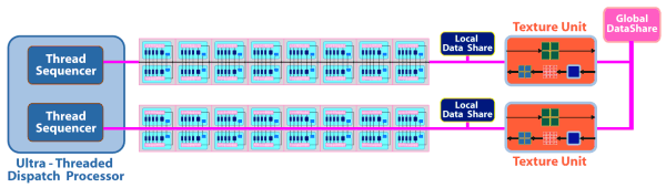 As we have already mentioned, each of ten SIMD cores contains 16 superscalar streaming processors (or 80 scalar ones), 16 KB of local memory to store data, and an individual dispatch processor. Besides, unlike R6x0 and RV670, TMUs are tied to a SIMD. Each of them has four dedicated texture units and L1 texture cache. The SIMD cores can exchange data using 16 KB of global memory. As we can see, the power of texture units in the new GPU is scaled together with the number of shader processors. ALUs relate to TMUs as 4:1. 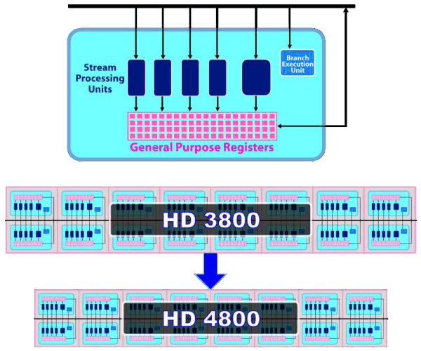 Streaming processors haven't changed since RV670, but their density has been increased (the picture is a scaled version). So the number of streaming processors was increased to 800 with the same fabrication process. More aggressive clock gating is used to raise energy efficiency. It allows to disable logic units to reduce power consumption. Besides, the superscalar design of streaming processors allowed AMD to implement support for double precision computing (FP64) using the same units in a more effective, easier way. As a result, RV770 offers much higher performance here, even though GT200 features special SPs for FP64 computing. The theoretical peak reaches 240 gigaflops. 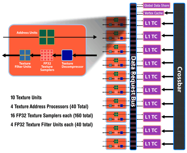 Texture units have been significantly overhauled. Now they are tied to SIMD, and their efficiency is improved. Engineers removed the dedicated TMU pool, available in previous generations. So the current solution is similar to what NVIDIA did with TMUs, included into SIMD cores. It's now impossible to fetch data without filtering, which could be done with vertex data. Texels and vertices are fetched by the same units in the new GPU, just like in the G8x and higher. On the other hand, each of 40 texture units in the RV770 is a tad weaker than each of 16 units in RV670. But there are more of them, and they operate at higher frequencies, so they should provide significant texturing performance gains. On the whole, one can expect up to 2.5-fold performance gains for bilinear filtering of 32-bit textures, and 1.25-fold gains for 64-bit textures. Other peculiarities -- doubled T-Cache bandwidth versus RV670, and fetching up to 160 texture samples (Fetch4/Gather4) per cycle, which must also raise performance. 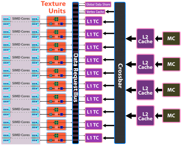 The chip uses a new design of caching units: separate vertex cache, L2 cache is tied to four 64-bit memory channels, L1 caches store unique data for each SIMD to raise caching efficiency. Bandwidth has grown as well: up to 480 GB/sec for L1 T-Cache, up to 384 GB/sec between L1 and L2 Caches. The above mentioned changes in texture units and caches make texturing performance of the RV770 twice as effective as in competing GPUs from NVIDIA (both G92 and GT200). Let's examine the ROP diagram: 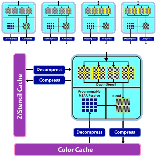 As we can see, there are not many qualitative changes in ROPs. Even though the number of ROPs hasn't changed since RV670, they can now process twice as many pixels per cycle in most cases, which is especially important for MSAA. Now algorithms of MSAA 2x and 4x come almost for "free", at least from the point of view of ROP operation. Here is a comparative table of the speed at which pixels are written into a frame buffer in various modes:  ROPs are twice as efficient almost in all modes, except for the simplest one -- 32-bit color without MSAA. We should also note Custom Filter Anti-Aliasing (CFAA). The previous generation of AMD GPUs offered special antialiasing filters called Custom Filter Anti-Aliasing. We analyzed this method in previous reviews. The most interesting antialiasing feature in AMD chips is edge detect used in CFAA 12x and 24x. This method offers the highest quality. It uses the shader power of RV670 and RV770 to process images, which already went through MSAA. The method consists in detecting polygon edges (special filter) and applying additional filtering to these image areas. It does not require additional video memory as in case of MSAA 4x and 8x, and it works together with adaptive antialiasing. RV770 features minor improvements to accelerate all methods. One of them is a special fast link between ROP and shader processors. We have information that RV770 does not use shader processors for MSAA, unlike R6xx and RV670. Standard MSAA algorithms use ROPs, only programmable CFAA uses shader resources. 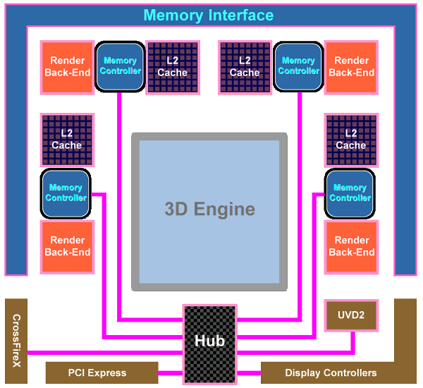 Another major change in the GPU is the upgrade from the widely advertized ring bus, which however was a failure, to the architecture with a central hub. Memory controllers in the RV770 are on the periphery of the chip, near the main traffic consumers. And the hub distributes data flows between the above mentioned units, as well as PCI Express, CrossFireX, UVD2, output controllers. According to the company's estimates, the new design of the memory interface significantly raised efficiency of bandwidth utilization. Besides, the controller supports new GDDR5 memory modules, operating at the frequency effectively quadrupled to 3.6-4 GHz and higher, which gives us memory bandwidth of up to 120 GB/sec with an inexpensive 256-bit interface. Prime costs are important, because a 512-bit bus is required to raise GDDR3 bandwidth, which leads to a larger GPU and its package. Cards themselves become bigger and more complex, consuming more power. Upgrading to GDDR5 allows to raise performance by 2-3 times and keep GPUs smaller, consuming less power. AMD was taking an active part in the development of GDDR5 standard together with all major memory manufacturers (Hynix, Qimonda, and Samsung) and JEDEC. This memory type took three years to develop, from the very beginning to the final specs. AMD spent even more time on this project. GDDR5 memory is planned to operate at up to 7 GHz of effective (quadrupled) frequency. The first 0.5-2 Gbit chips supporting 1.5 V (unlike 2.0 V for GDDR3) can operate at up to 1000*4=4.0 GHz. To conclude the architectural part of the review, we should publish the GPU diagram that shows GPU surface areas occupied by various units. As we can see, most part of the GPU is occupied by 800 streaming processors, a significant part of the chip is taken by texture processors and various controllers. To all appearances, the remaining part is occupied by ROPs, L2 Caches, and other auxiliary logic units. 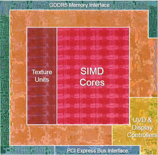 Just like in the GT200, the RV770 offers higher execution efficiency of geometry shaders, to be more exact -- higher speed of generating vertex data. The GPU supports four times as many geometry execution threads, lots of generated vertices can be stored in the GPU. The tessellator is also said to be modified. Now it's compatible with DirectX 10 and 10.1 (whatever it means), it also supports instancing. We shall have a look at the speed of executing geometry shaders in our synthetic tests in the next part of the review. The tessellator was described in the baseline review R600. Drawing a bottom line, we can say that the GPU can be called RV-"correction-of-mistakes"-770. All apparent bugs in the RV670 design were fixed. The number of ROPs hasn't changed, but they are twice as fast now, doing twice as much work per cycle in most cases. As a result, algorithms of MSAA 2x and 4x for RADEON HD 4800 come almost free of ROP charge, although memory bandwidth limitations may still reduce performance. These are not all changes. TMUs were also overhauled. The dedicated TMU pool was removed. The new solution includes TMUs into each of ten SIMD cores. Another major change is the upgrade of the ring bus to the hub architecture. It's interesting to note that almost all changes bring the RV770 GPU closer to what we see in NVIDIA solutions. It seems that ATI(AMD) have learned to admit their mistakes and fix them. Good of them. All we have to do now is to benchmark the new solutions. Write a comment below. No registration needed!
|
Platform · Video · Multimedia · Mobile · Other || About us & Privacy policy · Twitter · Facebook Copyright © Byrds Research & Publishing, Ltd., 1997–2011. All rights reserved. |


