NVIDIA GeForce Graphics Cards
|
Reference Information on NV4X Graphics Cards
Reference Information on G7X Graphics Cards
Reference Information on G8X Graphics Cards
G7X Specifications
| Code name |
G71 |
G73 |
G72 |
G70 |
| Baseline Article |
here |
here |
here |
| Process Technology (nm) |
90 |
110 |
| Transistors (M) |
279 |
178 |
112 |
302 |
| Pixel Processors |
24 |
12 |
4 |
24 |
| Texture Units |
24 |
12 |
4 |
24 |
| Blending Units |
16 |
8 |
2 |
16 |
| Vertex Processors |
8 |
5 |
3 |
8 |
| Memory Bus |
256 (64x4) |
128 (64x2) |
64 (32x2) |
256 (64x4) |
| Memory Types |
DDR, GDDR2, GDDR3 |
| System Bus |
PCI-Express 16x |
| RAMDAC |
2 x 400 MHz |
| Interfaces |
TV-Out
TV-In (a video capture chip is required)
2 x DVI Dual Link (cheaper models offer only one)
HDTV-Out |
| Vertex Shaders |
3.0 |
| Pixel Shaders |
3.0 |
| Precision of pixel calculations |
FP16
FP32 |
| Precision of vertex calculations |
FP32 |
| Texture Formats |
FP32 (without filtering)
FP16
I8
DXTC, S3TC
3Dc (emulation) |
| Rendering formats |
FP32 (without blending and MSAA)
FP16 (without MSAA)
I8
|
| MRT |
available |
| Antialiasing |
TAA (AA of transparent polygons)
2x and 4x RGMS
SS (in hybrid modes)
|
| Z generation |
2x without color |
| Stencil buffer |
Double-sided |
| Shadow technologies |
Hardware shadow maps
Geometry shadow optimizations |
Specifications of the G7X-based reference cards
| card |
chip
bus
|
PS/TMU/VS units |
Core frequency (MHz) |
Memory frequency (MHz) |
Memory capacity (MB) |
Memory bandwidth (GB) |
Texel rate (Mtex) |
Fill
rate (Mpix)
|
| GeForce 7800 GTX |
G70
PEG16x |
24/24/8 |
430 |
600(1200) |
256 GDDR3 |
38.4
(256) |
10320 |
6880 |
| GeForce 7800 GTX 512Mb |
G70
PEG16x |
24/24/8 |
550 |
850(1700) |
512 GDDR3 |
54.4
(256) |
13200 |
8800 |
| GeForce 7800 GT |
G70
PEG16x |
20/20/7 |
400 |
500(1000) |
256 GDDR3 |
32.0
(256) |
8000 |
6400 |
| GeForce 7800 GS |
G70
AGP |
16/16/6 |
375 |
600(1200) |
256 GDDR3 |
38.4
(256) |
6000 |
6000 |
| GeForce 7300 LE |
G72
PEG16x |
4/4/3 |
450 |
300(600) |
128 GDDR2 |
4.8
(64) |
1800 |
900 |
| GeForce 7300 GS |
G72
PEG16x |
4/4/3 |
550 |
350(700) |
256 GDDR2/GDDR3 |
5.6
(64) |
2200 |
1100 |
| GeForce 7300 GT |
G73
PEG16x |
8/8/4 |
350 |
333(667) |
128-256 GDDR3 |
10.7
(128) |
2800 |
1400 |
| GeForce 7600 GS |
G73
PEG16x |
12/12/5 |
400 |
400(800) |
256 GDDR2 |
12.8
(128) |
4800 |
3200 |
| GeForce 7600 GT |
G73
PEG16x |
12/12/5 |
560 |
700(1400) |
256 GDDR3 |
22.4
(128) |
6720 |
4480 |
| GeForce 7900 GTX |
G71
PEG16x |
24/24/8 |
650 |
800(1600) |
512 GDDR3 |
51.2
(256) |
15600 |
10400 |
| GeForce 7900 GT |
G71
PEG16x |
24/24/8 |
450 |
660(1320) |
256 GDDR3 |
42.2
(256) |
10800 |
7200 |
| GeForce 7900 GS |
G71
PEG16x |
20/20/7 |
450 |
660(1320) |
256 GDDR3 |
42.2
(256) |
9000 |
7200 |
| GeForce 7950 GX2 |
2xG71
PEG16x |
2x(24/24/8) |
500 |
600(1200) |
2x512 GDDR3 |
2x38.4
(2x256) |
2x12000 |
2x8000 |
| card |
chip
bus |
PS/TMU/VS units |
Core frequency (MHz) |
Memory frequency (MHz) |
Memory capacity (MB) |
Memory bandwidth (GB) |
Texel rate (Mtex) |
Fill
rate (Mpix) |
Details: G70, GeForce 7800 GTX
G70 Specifications
- Codename: G70 (previously known as NV47)
- Process technology: 110 nm (estimated manufacturer: TSMC)
- 302 million transistors
- FC package (flip-chip, flipped chip without a metal cap)
- 256 bit memory interface
- Up to 1 GB of GDDR3 memory
- PCI Express 16x
- 24 pixel processors, each of them has a texture unit with arbitrary filtering of integer and floating point FP16 textures (including anisotropy, up to 16x inclusive) and "free-of-charge" normalization of FP16 vectors. Pixel processors are improved in comparison with NV4X — more ALUs, effective execution of the MAD operation.
- 8 vertex processors, each of them has a texture unit without sample filtering (discrete sampling).
- Calculating, blending, and writing up to 16 full (color, depth, stencil buffer) pixels per clock
- Calculating and writing up to 32 values of Z buffer and stencil buffer per clock (if no color operations are performed)
- Support for a two-sided stencil buffer
- Support for special geometry render optimizations to accelerate shadow algorithms based on stencil buffer and hardware shadow maps (so called Ultra Shadow II technology)
- Everything necessary to support pixel and vertex Shaders 3.0, including dynamic branching in pixel and vertex processors, vertex texture fetch, etc.
- Texture filtering in FP16 format
- Support for a floating point frame buffer (including blending operations in FP16 format and only writing in FP32 format)
- MRT (Multiple Render Targets — rendering into several buffers)
- 2x RAMDAC 400 MHz
- 2 x DVI (external interface chips are required)
- TV-Out and HDTV-Out are built into the chip
- TV-In (an interface chip is required for video capture)
- Programmable streaming video processor (for video compression, decompression, and post processing), a new generation offering performance sufficient for high-quality deinterlacing HDTV
- 2D accelerator supporting all GDI+ functions
- SLI support
Reference card GeForce 7800 GTX specifications
- Core clock: 430 MHz
- Effective memory frequency: 1.2 GHz (2*600 MHz)
- Memory type: GDDR3, 1.6 ns
- Memory size: 256 MB (there also appeared a 512 MB modification with increased operating frequencies)
- Memory bandwidth: 38.4 GB/sec.
- Maximum theoretical fillrate: 6.9 gigapixel per second
- Theoretical texture sampling rate: 10.4 gigatexel per second
- 2 x DVI-I connectors
- SLI connector
- PCI-Express 16x bus
- TV-Out, HDTV-Out, HDCP support
- Power consumption: up to 110W (typical power consumption is below 100W, the card is equipped with one standard power connector for PCI Express, recommended PSUs should be 350W, 500W for SLI mode).
Continuity towards the previous flagships based on NV40 and NV45 is quite noticeable. Let's note the key differences:
- A finer process technology, more transistors, lower power consumption (even though there are more pipelines and the frequency is higher).
- There are 24 pixel processors instead of 16 (to be more exact, 6 quad processors instead of 4)
- Pixel processors have become more efficient — more ALUs, faster operations with scalar values and dot product/MAD.
- There are 8 vertex processors instead of 6. To all appearances, they are not modified.
- There appeared effective hardware support for HDTV video and HDTV-out, combined with TV-out.
So, the designers obviously pursued two objectives in the process of creating the new accelerator — to reduce power consumption and to drastically increase performance. As Shader Model 3.0 was already implemented in the previous generation of NVIDIA accelerators and the next rendering model (WGF 2.0) is not yet worked out in detail, this situation looks quite logical and expectable. Good news: pixel processors are not only increased in number, they also have become more efficient. We have just one question — why is there no filtering during texture sampling in vertex processors? This step seems quite logical. But this solution would probably have taken too much resources, so NVIDIA engineers decided to use them differently — to reinforce pixel processors and increase their number. The next generation of accelerators will comply with WGF 2.0 and will finally get rid of the disappointing asymmetry in texture unit capacities between vertex and pixel shaders.
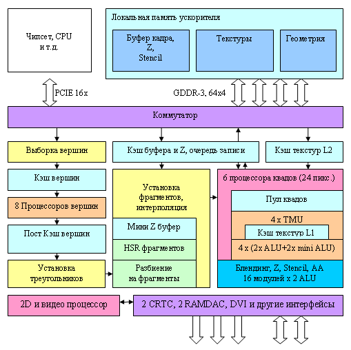
G70 Architecture
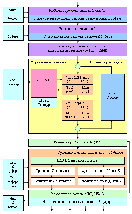
The key differences from NV45 are 8 vertex processors and 6 quad processors (all in all, 4*6=24 pixels are processed) instead of 4 with more ALUs for each processor. Pay your attention to the AA, blending, and writing unit, located outside the quad processor on the diagram. The fact is that even though the number of pixel processors is increased by 1.5, the number of modules responsible for writing the results remains the same — 16. That is the new chip can calculate shaders much faster, simultaneously for 24 pixels, but it still writes up to 16 full pixels per clock. It's actually quite enough — memory wouldn't cope with more pixels per clock. Besides, modern applications spend several dozens of commands before calculating and writing a single pixel. That's why increasing the number of pixel processors and retaining the same number of modules responsible for writing looks quite a balanced and logical solution. Such solutions were previously used in Low End NVIDIA chips (e.g. GeForce 6200), which had a sterling quad processor, but curtailed writing modules (in terms of the number of units and no FP16 blending).
Architecture of the pixel pipeline:
Have a look at the yellow unit of the pixel processor (quad processor). One can say that the architecture used in NV40/45 has been "turboed" — two full vector ALUs, which could execute two different operations over four components, were supplemented with two scalar mini ALUs for parallel execution of simple operations. Now ALUs can execute MAD (simultaneous multiplication and addition) without any penalty.
Adding small simplified and special ALUs is an old NVIDIA's trick, the company resorted to it several times to ensure noticeable performance gain in pixel units by only slightly increasing the number of transistors. For example, even the NV4X had a special unit for normalizing FP16[4] vectors (it is connected to the second main ALU and entitled FP16 NORM on the diagram). The G70 continues the tradition - such a unit allows considerable performance gain in pixel shaders due to free normalization of vectors each time a quad passes though a pipeline of the processor. Interestingly, the normalization operation is coded in shaders as a sequence of several commands, the driver must detect it and substitute it with a single call to this special unit. But in practice this detection process is rather efficient, especially if a shader was compiled from HLSL. Thus, NVIDIA's pixel processors don't spend several clocks on vector normalization as ATI does (it's important not to forget about the format limitation - FP16).
What concerns texture units, everything remains the same — one unit per pixel (that is four units in a quad processor), native L1 Cache in each quad processor, texture filtering in integer or FP16 component format, up to 4 components inclusive (FP16[4]). Texture sampling in FP32 component format is possible only without hardware filtering — you will either have to do without it or program it in a pixel shader, having spent a dozen of instructions or more. However, the same situation happened before - sterling support for FP32 components will probably be introduced only in the next generation of architectures.
The array of six quad processors is followed by the dispatch unit, which redistributes calculated quads among 16 Z, AA, and blending units (to be more exact, among 4 clusters of 4 units, processing an entire quad - geometric consistency must not be lost, as it's necessary to write and compress color and Z buffer.) Each unit can generate, check, and write two Z values or one Z value and one color value per clock. Double-sided stencil buffer operations. Besides, one such unit executes 2x multisampling "free-of-charge", 4x mode requires two passes through this unit, that is two clocks. Let's sum up features of such units:
- Writing colors — FP32[4], FP16[4], INT8[4] per clock, including MRT.
- Comparing and blending colors — FP16[4], INT8[4], FP32 is not supported as a component format
- Comparing, generating, and writing the depth value (Z) — all modes; two values per clock in Z-only mode. In MSAA mode — two values per clock as well.
- MSAA — INT8[4], not supported for floating point formats.
There appear so many conditions due to many hardware ALUs, necessary for MSAA operations, generating Z-values, comparing and blending color. NVIDIA tries to optimize transistor usage and employs the same ALUs for different purposes depending on a task. That's why the floating point format excludes MSAA and FP32 excludes blending. High transistor usage is one of the reasons to preserve 16 units instead of upgrading to 24 ones according to the number of pixel processors. In this case the majority of transistors in these units may (and will) be idle in modern applications with long shaders even in 4xAA mode. Memory, which pass band has not grown compared to the GeForce 6800 Ultra, will not allow to write even 16 full pixels into a frame buffer per clock anyway. As these units are asynchronous to pixel processors (they are calculating Z-values and blending, when shaders calculate colors for the next pixels), 16 units are a justified, even obvious solution. Some restrictions due to FP formats are disappointing but typical of our transition period on the way to symmetric architectures, which will allow all operations with all available data formats without any performance losses, as allowed by flexible modern CPUs in most cases.
Vertex Pipeline Architecture
We've already seen everything in the NV4x family, only the number of vertex processors is increased from 6 to 8.
Details: G71, GeForce 7900 GT/GeForce 7900 GTX/GeForce 7950 GX2
G71 Specifications
- Codename: G71
- Process technology: 90 nm (estimated manufacturer: TSMC)
- 279 million transistors (that is fewer than in G70)
- FC package (flip-chip, flipped chip without a metal cap)
- 256 bit memory interface, four-channel controller
- Up to 1 GB of GDDR3 memory
- PCI Express 16x
- 24 pixel processors, each of them has a texture unit with arbitrary filtering of integer and floating point FP16 textures (including anisotropy, up to 16x inclusive) and "free-of-charge" normalization of FP16 vectors (improved modification of NV4X — more ALUs, efficient MAD execution).
- 8 vertex processors, each of them has a texture unit without sample filtering (discrete sampling).
- Calculating, blending, and writing up to 16 full (color, depth, stencil buffer) pixels per clock
- Calculating and writing up to 32 values of Z buffer and stencil buffer per clock (if no color operations are performed)
- Support for two-sided stencil buffer
- Support for special geometry render optimizations to accelerate shadow algorithms based on stencil buffer and hardware shadow maps (so called Ultra Shadow II technology)
- Everything necessary to support pixel and vertex Shaders 3.0, including dynamic branching in pixel and vertex processors, vertex texture fetch, etc.
- Texture filtering in FP16 format
- Support for a floating point frame buffer (including blending operations in FP16 format and only writing in FP32 format)
- MRT (Multiple Render Targets — rendering into several buffers)
- 2 x RAMDAC 400 MHz
- 2 x DVI interfaces (Dual Link, 2560x1600 support, the interfaces are integrated into G71, so there is no need in external interface chips)
- TV-Out and HDTV-Out are built into the chip
- TV-In (an interface chip is required for video capture)
- Programmable streaming video processor (for video compression, decompression, and post processing), a new generation offering performance sufficient for high-quality HDTV deinterlacing. Sterling hardware acceleration for H.264, WMV-HD, etc.
- 2D accelerator supporting all GDI+ functions
Reference card GeForce 7900 GTX specifications
- Core clock: 650 MHz (pixel processors and blending)
- Vertex Unit Frequency: 700 MHz
- Effective memory frequency: 1.6 GHz (2*800 MHz)
- Memory type: GDDR3, 1.1ns (standard frequency is up to 2*900 MHz)
- Memory: 512 MB
- Memory bandwidth: 51.2 GB/sec.
- Maximum theoretical fillrate: 10.4 gigapixel per second.
- Theoretical texture sampling rate: 15.6 gigatexel per second.
- 2 x DVI-I (Dual Link, 2560x1600 video output)
- SLI connector
- PCI-Express 16x bus
- TV-Out, HDTV-Out, HDCP support
- Power consumption: noticeably lower than in GeForce 7800 (something about 70-80 Watt, but exact figures are not published).
Reference card GeForce 7900 GT specifications
- Core clock: 450 MHz (pixel processors and blending)
- Vertex Unit Frequency: 470 MHz
- Effective memory frequency: 1.32 GHz (2*660 MHz)
- Memory type: GDDR3, 1.4ns (standard frequency is up to 2*700 MHz)
- Memory: 256 MB
- Memory bandwidth: 42.2 GB/sec.
- Maximum theoretical fillrate: 7.2 gigapixel per second.
- Theoretical texture sampling rate: 10.8 gigatexel per second.
- 2 x DVI-I (Dual Link, 2560x1600 video output)
- SLI connector
- PCI-Express 16x bus
- TV-Out, HDTV-Out, HDCP support
- Power consumption: noticeably lower than in GeForce 7800 (something about 50-60 Watt, but exact figures are not published).
Reference card GeForce 7950 GX2 Specifications
- Core clocks: 2 x 500 MHz (pixel processors and blending)
- Vertex unit frequency: 2 x 500 MHz
- Effective memory frequency: 1.2 GHz (2*600 MHz)
- Memory type: GDDR3, 1.4ns (standard frequency is up to 2*700 MHz)
- Memory: 2 x 512 MB
- Memory bandwidth: 2 x 38.4 GB/sec.
- Maximum theoretical fillrate: 2 x 8 gigapixel per second.
- Theoretical texture sampling rate: 2 x 12 gigatexel per second.
- 2 x DVI-I (Dual Link, 2560x1600 video output)
- SLI connector
- PCI-Express 16x bus
- TV-Out, HDTV-Out, HDCP support
- It consumes much more power than GeForce 7800 and 7900 cards (probably more than 100 Watt, exact data are not available).
That's obviously the same architecture as in G70, it's just manufactured by the 90nm process technology with minor changes. For some reason, the number of transistors is noticeably reduced, but it has no effect on performance. Perhaps, G70 had some units in reserve (for example, it might have 7-8 pixel processor quads instead of 6, 9-10 vertex units instead of 8) to increase the yield of effective chips or even to manufacture an Ultra modification, if the competitors had launched a higher-performance model.
To all appearances, a number of units in the new G71 is maximized - either the yield of effective chips manufactured by the 90nm process technology is that high, or NVIDIA can afford more rejects (as the cost of this chip dropped due to its much smaller surface area). There is also another answer to this question - good optimization. But it's less probable, because it's difficult to reduce the number of transistors by 25 millions without any performance loss and preserve the same architecture. But it may be possible, so let's not discard this version from the very beginning. So, there are indirect signs of high yield of effective chips and no manufacturing problems, as well as much lower costs of the new chip compared to G70. Hence the codename - G71, this chip is indeed inferior to G70 in transistors. From the architectural point of view, it offers the same features and the same number of active units. It's all up to the clock frequency, which is much higher here.
Note two integrated Dual Link DVI interfaces - the times of external interface chips are gone. The 400 MHz specifications on RAMDAC are not developed any more - why make it higher, analog monitors have stopped their development. The company declares hardware support for H.264 and other video encoding formats of the latest generations. Interestingly, this feature was also supported by the NV4X family. But some bug made it unavailable to NV40 and NV45. What concerns new chips (NV43, etc), it can be enabled in the new drivers. Along with decoding, we are again promised an improved deinterlacing algorithm and new post processing providing sharper image and better color rendition.
There is an interesting dual-chip modification of G71 - GeForce 7950 GX2 that appeared much later than single-chip cards. In fact, it's two GeForce 7900 GTX chips operating at reduced frequencies in SLI mode on a single card. That is two G71 accelerators operate in a single slot. The price of compact dimensions (compared to two 7900 GTX cards) is reduced operating frequencies, both of memory and of the chips. It's impossible to arrange the chips in a semicircle around the core. So the chips will be at different distances from the GPU, which implies some limitations. Engineers of the dual-GPU card had to use very thin coolers, which limited the range of GPU frequencies, so it was reduced from 650 MHz to 500 MHz. Only the low power consumption and heat release of the G71 chip made it possible to design such a dual-GPU flagship. As neither G70 nor R580 would have allowed to design such a card within the modern PC specifications on power consumption and heat release.
Interestingly, such a card does not require SLI support from a motherboard. Everything necessary is on the card itself. The card consists of two PCBs: master and slave. It's two slots wide. In Quad-SLI mode, the card is connected to the neighboring dial-GPU card via two links. Two components are responsible for SLI: a chip on the second PCB - a modified HSI bridge (PCIE-to-PCIE) and an adapter installed into special connectors on both parts of the card. As a result, we got a compact solution, which can be installed into any standard modern PC case.
If performance of a single GeForce 7950 GX2 card is not enough, you can use two such cards in Quad-SLI mode with a SLI motherboard and a very powerful PSU (support for this mode appeared in Drivers 91.37). Thus, NVIDIA offers a single-card SLI solution as well as an opportunity to upgrade it to Quad-SLI by installing the second card.
It still works as before - there are three cooperative modes - AFR (Alternative Frame Rendering), Slicing (splitting a frame into four zones) and SLI-AA - using accelerators to calculate different AA samples in a single pixel. Besides, it's logical to combine the modes - for example, 2xAFR from two two-zone frames (Alternative Frame Rendering, where each frame is formed by SLI slicing) or 2x SLI-AA slicing, etc. There can be many combinations, but no new architectural changes are necessary - SLI already offers many features, their combinations are controlled by the driver.
Details: G73, GeForce 7600 GT/GeForce 7600 GS
G73 Specifications
- Codename: G73
- Process technology: 90 nm (estimated manufacturer: TSMC)
- 178 million transistors
- FC package (flip-chip, flipped chip without a metal cap)
- 128 bit memory interface (dual channel controller)
- Up to 512 MB of GDDR3 memory
- PCI Express 16x
- 12 pixel processors, each of them has a texture unit with arbitrary filtering of integer and floating point FP16 textures (including anisotropy, up to 16x inclusive) and "free-of-charge" normalization of FP16 vectors (improved modification of NV4X — more ALUs, efficient MAD execution).
- 5 vertex processors, each of them has a texture unit without sample filtering (discrete sampling).
- Calculation, blending, and writing of up to 8 full (color, depth, stencil buffer) pixels per clock
- Calculating and writing up to 16 values of Z buffer and stencil buffer per clock (if no color operations are performed)
- Support for a two-sided stencil buffer
- Support for special geometry render optimizations to accelerate shadow algorithms based on stencil buffer and hardware shadow maps (so called Ultra Shadow II technology)
- Everything necessary to support pixel and vertex Shaders 3.0, including dynamic branching in pixel and vertex processors, vertex texture fetch, etc.
- Texture filtering in FP16 format
- Support for a floating point frame buffer (including blending operations in FP16 format and only writing in FP32 format)
- MRT (Multiple Render Targets — rendering into several buffers)
- 2 x RAMDAC 400 MHz
- 2 x DVI Dual Link interfaces (2560x1600 support, the interfaces are integrated into G73, so there is no need in external interface chips)
- TV-Out and HDTV-Out are built into the chip
- TV-In (an interface chip is required for video capture)
- Programmable streaming video processor (for video compression, decompression, and post processing), a new generation offering performance sufficient for high-quality HDTV deinterlacing. Sterling hardware acceleration for H.264, WMV-HD, etc.
- 2D accelerator supporting all GDI+ functions
Reference card GeForce 7600 GT specifications
- Core clock: 560 MHz (pixel processors and blending)
- Vertex Unit Frequency: 560 MHz
- Effective memory frequency: 1.4 GHz (2*700 MHz)
- Memory type: GDDR3, 1.4ns (standard frequency is up to 2*700 MHz)
- Memory: 256 MB
- Memory bandwidth: 22.4 GB/sec.
- Maximum theoretical fillrate: 4.48 gigapixel per second.
- Theoretical texture sampling rate: 6.72 gigatexel per second.
- 2 x DVI-I (Dual Link, 2560x1600 video output)
- SLI connector
- PCI-Express 16x bus
- TV-Out, HDTV-Out, HDCP support
- It consumes very little power (something about 40-60 Watt, but exact data are not available).
Reference GeForce 7600 GS Specifications
- Core clock: 400 MHz (pixel processors and blending)
- Vertex Unit Frequency: 400 MHz
- Effective memory frequency: 0.8 GHz (2*400 MHz)
- Memory type: DDR2, 2.5ns (standard frequency: up to 2*400 MHz)
- Memory: 256 MB
- Memory bandwidth: 12.8 GB/sec.
- Maximum theoretical fillrate: 3.2 gigapixel per second.
- Theoretical texture sampling rate: 4.8 gigatexel per second.
- 2 x DVI-I (Dual Link, 2560x1600 video output)
- SLI connector
- PCI-Express 16x bus
- TV-Out, HDTV-Out, HDCP support
- Power consumption: lower than in GeForce 7600 GT
G73 is evidently a half (except for 5 instead of 4 vertex units) of G71. Both in terms of the memory controller as well as the pixel part. But we should make a reservation here - according to our tests, G73 physically has 16 pixel processors, not 12 (that is it has 4 quads). One quad is retained to increase the yield of effective chips or (you never can tell) for a future solution with 16 pixel units to oppose a new competitor on the market. The surface area of the chip is smaller than in NV43, but the chip is much more efficient.
G74 codename is not used yet - to all appearances, it can be used for a cheaper G71 reincarnation. It can also be designed for 20 or 16 pixel pipelines.
Details: G72, GeForce 7300 GS
G72 Specifications
- Codename: G72
- Process technology: 90 nm (estimated manufacturer: TSMC)
- 112 million transistors
- FC package (flip-chip, flipped chip without a metal cap)
- 64 bit memory interface (dual channel controller)
- Up to 512 MB of DDR2/GDDR3 memory
- PCI Express 16x
- 4 pixel processors, each of them has a texture unit with arbitrary filtering of integer and floating point FP16 textures (including anisotropy, up to 16x inclusive) and "free-of-charge" normalization of FP16 vectors (improved modification of NV4X — more ALUs, efficient MAD execution).
- 3 vertex processors, each with a texture unit, without filtering samples (discrete sampling).
- Calculating, blending, and writing up to 2 full (color, depth, stencil buffer) pixels per clock
- Calculating and writing up to 4 values of Z buffer and stencil buffer per clock (if no color operations are performed)
- Support for a two-sided stencil buffer
- Support for special geometry render optimizations to accelerate shadow algorithms based on stencil buffer and hardware shadow maps (so called Ultra Shadow II technology)
- Everything necessary to support pixel and vertex Shaders 3.0, including dynamic branching in pixel and vertex processors, vertex texture fetch, etc.
- Texture filtering in FP16 format
- Support for a floating point frame buffer (including blending operations in FP16 format and only writing in FP32 format)
- MRT (Multiple Render Targets — rendering into several buffers)
- 2 x RAMDAC 400 MHz
- DVI Dual Link supporting up to 2560x1600 video output, this interface is integrated into the chip, so an external interface chip is not necessary)
- TV-Out and HDTV-Out are built into the chip
- TV-In (an interface chip is required for video capture)
- Programmable streaming video processor (for video compression, decompression, and post processing), a new generation offering performance sufficient for high-quality HDTV deinterlacing. Sterling hardware acceleration for H.264, WMV-HD, etc.
- 2D accelerator supporting all GDI+ functions
Reference GeForce 7300 GS Specifications
- Core clock: 550 MHz (pixel processors and blending)
- Vertex Unit Frequency: 550 MHz
- Effective memory frequency: 0.7 GHz (2*350 MHz)
- Memory type: DDR2, 2.8ns (standard frequency: up to 2*350 MHz)
- Memory: 256 MB
- Memory bandwidth: 5.6 GB/sec.
- Maximum theoretical fillrate: 1.1 gigapixel per second.
- Theoretical texture sampling rate: 2.2 gigatexel per second.
- Support Dual Link DVI-I, 2560x1600 video output
- PCI-Express 16x bus
- TV-Out, HDTV-Out, HDCP support
- Power consumption: very low
This G7x-series modification has even fewer units - only four pixel processors and four texture units, three vertex processors, and two ROPs. In other respects, the card is just like the other models in the family from other price segments, the architecture is practically the same. There may be some changes in cache sizes and the like, but we cannot say anything more specific, we can only speculate.
Interestingly, later on there appeared GeForce 7300 GT card, it wasn't based on G72, as you might have assumed; it was based on the de-featured and slowed-down G73, that is on the chip used in the GeForce 7600 series. But pixel units of the GPU were cut down from 12 to 8. And it has one active vertex unit down. I wonder why this card hasn't been called GeForce 7600 LE or XT. This name would have been much better.
Reference Information on NV4X Graphics Cards
Reference Information on G7X Graphics Cards
Reference Information on G8X Graphics Cards
Write a comment below. No registration needed!
|
|
 |
|
|
|