 |
||
|
||
| ||
|
||
|
||
| ||
Reference Information on NV4X Graphics Cards G8X/G9X Specifications
Specifications of the G8X-based reference cards
Details: G80, GeForce 8800 SeriesG80 Specifications
Specifications of the Reference GeForce 8800 GTX
Specifications of the Reference GeForce 8800 GTS
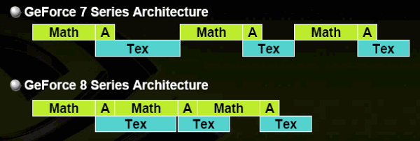
ArchitectureWe've been looking forward to the upgrade to unified graphics architectures for a long time. Now we can establish a fact - GeForce 8800 has done it, the critical line has been crossed. Such architectures will now gradually go down to the Middle and Low End segments. They will then be merged with multi-core processor architectures in distant future. Let's meet the first unified architecture from NVIDIA: 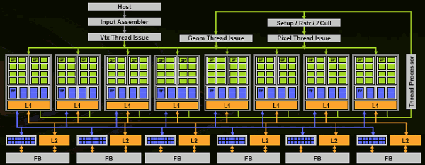 Here is the entire diagram of the GPU. The chip consists of 8 unified shader processors. Although NVIDIA speaks of 128 processors (each ALU being a processor), this is not entirely true. A command execution unit is a processor unit consisting of 4 TMUs and 16 ALUs. Thus, we have 128 ALUs and 32 TMUs all in all. But the execution granularity is 8 units. Each of them can execute a part of a vertex/pixel/geometry shader over a group of 32 pixels (or the corresponding number of vertices and other primitives). All branches, jumps, conditions, etc are applied to a single unit. Thus, it's only logical to call this unit a shader processor, even if very wide. Each processor has its own L1 cache, which stores not only textures, but also other data that can be requested by a shader processor. You should understand that the main stream of data (for example, pixels or vertices, processed moving in a circle under control of the Thread Processor) is not cached. Data flow is a stream, that's the main attraction of the new graphics architectures - no random access on the level of processed primitives. Along with the thread processor and 8 shader processors, there are 6 ROPs that calculate visibility, write data into a frame buffer, and do MSAA (the blue units near the L2 Caches), grouped with memory controllers, write queues, and L2 Cache. Thus we get a very wide (8 units, each one processing a chunk of 32 pixels) architecture that can scale well both ways. System bandwidth will be controlled by adding or removing memory controllers and shader processors, so the balance will not be broken and no bottlenecks will be created. It's a nice logical solution that uses the key advantage of a unified architecture - automatic balance and high efficiency of available resources. Along with shader units and ROPs, there are also a number of administrative units:
Let's digress a little: these units will get more generic in future, they won't be tied to a specific type of shaders. That is they will become all-purpose units that will initiate data computations and format conversions - for example, from one shader to another, from a vertex shader to a pixel one, etc. It won't require any principal changes in the architecture. The diagram will look and work practically the same, except for fewer special "grey" units. Even now all three Thread Issues are actually a single unit with common functionality and context additions: 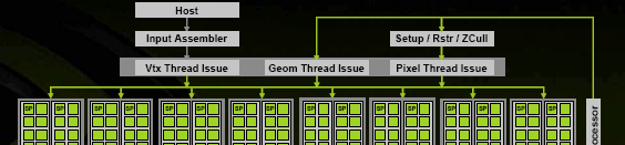 Shader processor and its TMU/ALU
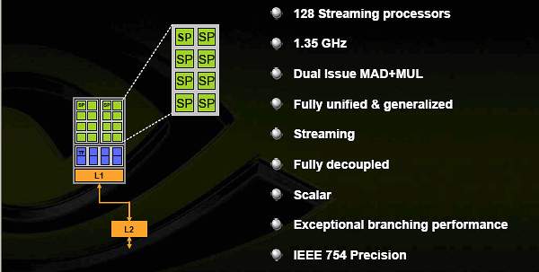 So, each of the eight shader units has 16 scalar ALUs. That's another potential possibility to increase their load efficiency up to 100% regardless of shader code. ALUs operate at the double frequency. Thus, they match or even outperform (depending on operations in a shader) 8 old quad-component vector ALUs (G70) operating at the same core clock. NVIDIA publishes the following calculations of peak performance: 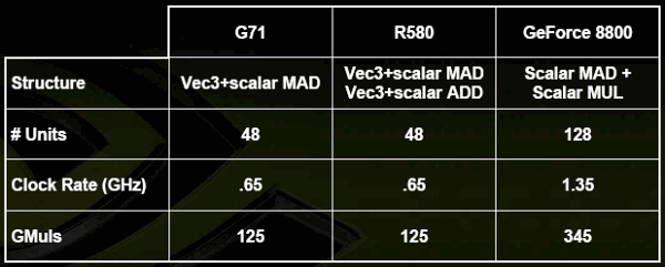 But they are true for the worst case scenario for the other GPUs - two multiplications. In real life you should divide this advantage by about 1.5. Anyway, these scalar ALUs outperform all older chips owing to their higher clock rate and quantity. Perhaps except for the G71 SLI configuration with certain shaders that do not favor the new architecture. Interestingly, all ALUs have the FP32 precision. Considering the new architecture, we don't see any advantages for FP16 shaders with reduced precision. One more interesting issue - support for computations in integer format. This one is necessary for SM4. Arithmetic is implemented in compliance with IEEE 754, which makes it suitable for serious non-gaming computing - scientific, statistic, economic, etc. Now what concerns interaction between texture units and ALUs inside the same shader unit:
 Texture sampling and filtering do not require ALU resources. They can now be performed simultaneously with computations. But texture addressing (P on the diagram) still takes up some ALU time. It's logical, if we want to use GPU transistors hundred-per-cent - texture addressing requires standard floating-point operations, and it wouldn't have been wise to have dedicated ALUs for it. Texture modules themselves have the following configuration:
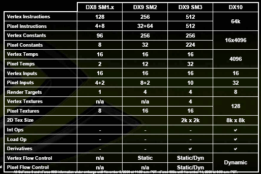
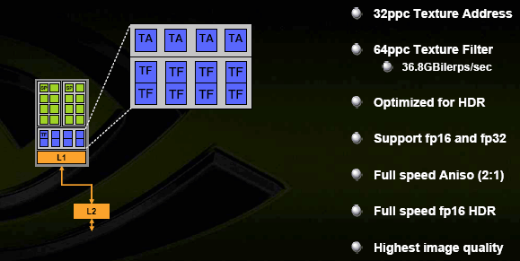 There are four TA units (texture address) and twice as many TF units for bilinear texture filtering. Why so? It does not require many transistors and provides free honest trilinear filtering or allows to half the performance drop for anisotropic filtering. Performance in usual resolutions with usual filtering without AA is not relevant anymore - the previous generation of graphics cards copes well with this load. The new GPU supports FP16/FP32 texture formats and SRGB gamma correction at the input (TMU) and output (ROP). Here are specifications of Shader Model 4 of the new GPUs:
 ROPs, frame buffer, antialiasingAs you may remember, along with eight shader units, there are also six ROPs:
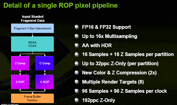 The diagrams show two routes for Z and C. But in fact it's just the same set of ALUs, which are divided into two groups to process pixels with color, or act as a single group to process them in Z-Only mode thus doubling the bandwidth. It makes no sense to count single pixels these days - there are more than enough of them. It's much more important to count how many MSAA samples can be processed per cycle. Thus, the GPU can provide six sterling pixels per cycle in MSAA 16x mode, in 8x mode - 12 pixels, etc. Interestingly, scalability of operations with a frame buffer is up to the mark - as you can remember, each ROP works with its own memory controller and does not interfere with other units. There finally appeared sterling support for FP32 and FP16 formats of the frame buffer with antialiasing. The sky is the limit to imagination of game developers, and HDR does not require changes in the frame rendering order even in AA mode. CSAAThere also appeared a new antialiasing method - CSAA. We'll soon publish its detailed description on the web site. As for now, we can say that it's similar to ATI's approach, it also deals with pseudo stochastic patterns and propagation of samples to neighboring geometric zones (a pixel is spread out, pixels do not have sharp borders, they sort of blend into each other from the point of view of AA, covering some area). Color and Z values of colors are stored separately from their addresses. Thus, there may be up to 16 samples per pixel, but, for example, only eight Z values - it saves bandwidth and cycles. Classic MSAA in modes exceeding 4x requires much memory, while its quality does not grow much. The new method corrects it. It allows AA 16x of much higher quality than MSAA 16x with arithmetic expenses comparable to 4x MSAA. NVIOAnother new feature in the G80 is its interfaces - they are implemented outside the main GPU. A stand-alone chip called NVIO is responsible for them now:  This chip integrates:
The output system looks like this: 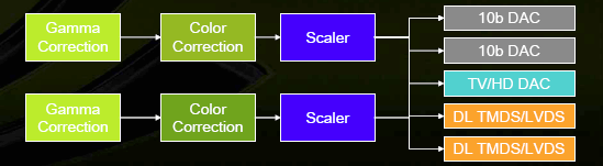 Precision is always 10 bit per component. This stand-alone chip may not survive in the Mid- and Low-End segments. But this solution has more pros than cons for expensive cards. Interfaces take up a significant part of the chip, they depend much on interferences, they require special power supply. A stand-alone chip may solve these problems as well as improve the quality of output signals and configuration flexibility. Besides, engineers won't have to take into account optimal modes for built-in RAMDACs, so it will not complicate the development process of this already complex chip. Details: G84/G86, GeForce 8600 and 8500 SeriesG84 Specifications
Specifications of the Reference GeForce 8600 GTS
Specifications of the Reference GeForce 8600 GT
G86 Specifications
Specifications of the Reference GeForce 8500 GT
G84 and G86 ArchitectureWe can see in the specifications that G84 stands in between 1/4 and 1/3 of G80 the flagship. It's 1/4 in terms of unified processors, and it's 1/3 in terms of ROPs and memory controller. What concerns texture units, the situation is vague - it's not 1/4, but it's not 1/2. We'll speak about it below. In its turn, G86 is something very interesting - it's only 1/8 of G80 in terms of computing power, but it's 1/3 in terms of ROPs. NVIDIA is evidently not in a hurry to send fast GPUs down to Low-End. The main question here is whether 1/4 and 1/8 are enough to compete with the existing solutions and future GPUs from AMD. Did NVIDIA cut down the number of units too much? We cannot say that both GPUs have few transistors... G84 has almost half of transistors available in G80, G86 - almost one third. It looks like a trade-off solution. If the designers had preserved half of G80 units, the GPU would have been too expensive to manufacture, and it would have competed with the GeForce 8800 GTS. In the nearest future the 65nm process technology will most likely be used for faster Mid- and Low-End GPUs. As for now, it's all we've got. We'll analyze performance of the new GPUs in synthetic and game tests. But even now we can say that G84 and G86 may be not fast enough because of few ALUs. They will most likely be on a par with the existing solutions at similar prices. We'll not describe the architecture of G84 and G86 in much detail. There are only few changes compared to G80. Everything written about the GeForce 8800 holds true corrected for the quantitative characteristics. But we'll cover the key issues and publish several slides about architectural specifications of the new GPUs. G80 consists of eight unified shader processors, but NVIDIA prefers to speak of 128 processors. To all appearances, a command execution unit is an entire processor consisting of four TMUs and 16 ALUs. Each unit can execute a part of a vertex, pixel, or geometry shader with 32 pixels, vertices, or other primitives. It can also compute physics. Each processor has its L1 cache to store textures and other data. Along with the thread processor and shader processors, there are six ROPs that calculate visibility, write data into a frame buffer, and do MSAA, grouped with memory controllers, write queues, and L2 Cache. This architecture can scale well both ways, which has been done in the new solutions. We've already mentioned this elegant solution that uses the main advantage of the unified architecture - automatic balance and high efficiency of available resources in the article about the GeForce 8800. We also assumed there that a Mid-End solution would comprise half of computing units. And the budget solution will have two shader processors and one ROP. Unfortunately, the new GPUs have fewer units than we had initially expected, unlike the GeForce 8800 with its eights processors (32 TMUs and 128 ALUs). To all appearances, the diagram of G84 looks like this:  That is everything remains unchanged, except for a number of units and memory controllers. There are minor changes that have to do with texture units. You can see them in this picture, but we'll talk about them later. I wonder where all these transistors are gone, if G84 has only 32 processors? G84 has almost half of the transistors available in G80, but it has much fewer memory channels, ROPs, and shader processors. G86 also has many transistors and just 16 processors... I also wonder how well the balance between vertex/pixel/geometry shaders will be in real applications there are much fewer unified executing units now. Especially as the unified architecture itself sets new tasks to developers. They will have to decide upon efficient distribution of the GPU capacities between vertex, pixel, and geometry shaders. Here is a simple example - focus on computing pixels. Heavier load on vertex units in the traditional architecture will not result in a performance drop in this case. What concerns the unified architecture, it will change the balance and cut down resources allocated to pixel computations. We shall analyze the performance issue in future. And now we'll continue our review of changes in the G84/G86 architecture. Shader processor and TMU/ALUThe diagram of shader units and evaluation of their peak computing performance in G80 was published in the corresponding article. Nothing has changed for G84 and G86, and their performance is easy to recalculate. ALUs in these GPUs also operate at double frequency. They are scalar units, so they can reach a high efficiency factor. There are no differences in functionality either. All ALUs have the FP32 precision, they support integer computing. They comply with IEEE 754, which is important for scientific, statistic, economic, and other computations. But texture units have changed. According to NVIDIA, the new GPUs were modified to increase performance of the unified processors. Each texture unit in G80 could compute four texture addresses and perform eight texture filtering operations per cycle. They say that the new GPUs can do twice as many texture addresses and texture fetches. That is texture units in G84 and G86 have the following configuration (the diagram of these units in G80 is published on the left):  The other functionality of texture units is identical, they support FP16/FP32 texture formats, etc. But G80 can filter FP16 textures at full speed owing to twice as many filtering units. Mid- and Low-End solutions cannot do it (given the above-mentioned changes really exist.) ROPs, frame buffer, antialiasingROPs (eight units in G80, two units in the new GPUs) haven't changed:  A new antialiasing method is supported - Coverage Sampled Antialiasing (CSAA). We've already seen it in GeForce 8800, and it was described in detail in the corresponding article:
In brief, color and Z values of samples are stored separately from information about their location. There can be up to 16 samples and just 8 Z values per pixel - it saves bandwidth and cycles. CSAA allows to do with transmitting and storing a single color value or Z value per each subpixel. It specifies more accurately the averaged value of a screen pixel by using precise information how this pixel covers triangle borders. As a result, the new method performs 16x antialiasing of noticeably higher quality than MSAA 4x at the same computational expenses. In rare cases, when CSAA does not work, we get usual MSAA of lower degree instead of no antialiasing at all. PureVideo HDWe proceed to the most interesting changes. G84 and G86 have new features that are not available in G80! They have to do with the built-in video processor, which enjoys extended support for PureVideo HD in the new GPUs. These GPUs fully offload a CPU, when they decode all popular types of video data, including H.264. G84 and G86 use a new model of programmable PureVideo HD processor. It's more powerful than the one used in G80 and includes the BSP engine. The new processor can decode H.264, VC-1, and MPEG-2 formats with the resolution of up to 1920x1080 and the bitrate of up to 30-40 Mbit/s. It does all the work on decoding CABAC and CAVLC data on the hardware level, so you can play all existing HD-DVD and Blu-ray discs even on mediocre single-core PCs. The video processor in G84/G86 consists of several parts: Video Processor itself of the second generation (VP2) - it performs IDCT tasks, motion compensation, and deblocking for MPEG2, VC-1, and H.264 formats, and supports hardware decoding of the second stream; Bitstream Processor (BSP) - it performs statistic decoding CABAC and CAVLC for H.264 (these are ones of the heaviest operations); AES128 engine - it decrypts video data used for copy protection in Blu-ray and HD-DVD discs. Here are the differences in hardware support for video decoding in various GPUs: 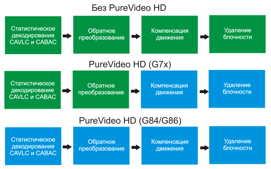 The new features of PureVideo HD worked only in the 32-bit version of Windows Vista at the time of the announcement. PureVideo HD will appear in Windows XP only in summer. What concerns the quality of video playback, post processing, deinterlacing, etc, NVIDIA improved the situation since GeForce 8800. And there is nothing peculiar about the new chips in this respect. CUDA, computing non-gaming data and physicsThe article about GeForce 8800 mentioned that the increased peak performance of floating-point arithmetic operations in the new graphics cards and flexibility of the unified shader architecture became sufficient to compute physics in games and even in serious applications: mathematical and physical modelling, economic and statistic models and calculations, OCR, image processing, science graphics, and many others. A special API for computing was released. It's convenient to adapt and develop programs that offload computing to a GPU - CUDA (Compute Unified Device Architecture). You can read about CUDA in the article about G80. We'll dwell on another fashionable trend these days - support for computing physics on GPU. NVIDIA calls this technology Quantum Effects. It's declared that all GPUs of the new generation, including G84 and G86, cope well with such computations. They allow to take some CPU load to a GPU. Some examples include simulations of smoke, fire, explosions, hair/cloth/fur/fluid dynamics, etc. But we'd like to write about another thing. That we are shown only images from test applications with many physical objects computed by a GPU. Games with this support are nowhere to be found.  Support for external interfacesAs you may remember, we were surprised by one more unexpected innovation in GeForce 8800 - an additional chip that supports external interfaces. A separate chip called NVIO is responsible for these tasks in top graphics cards, which integrates the following: 2 x 400 MHz RAMDAC, 2 x Dual Link DVI (or LVDS), HDTV-Out. Even at that time we already assumed that a separate external chip would hardly survive in Mid- and Low-End solutions. And that's what really happened. Support for all these interfaces is built into a GPU itself in G84 and G86. GeForce 8600 GTS comes with two Dual Link DVI-I outputs with HDCP support. It's the first graphics card on the market with such features (HDCP and Dual Link at the same time). What concerns HDMI, support for this connector is fully implemented on the hardware level. It can be used by manufacturers in non-reference graphics cards. But support for HDCP and HDMI is optional in GeForce 8600 GT and 8500 GT. They can still be implemented by some manufacturers in their products. Details: G92, GeForce 8800 SeriesG92 Specifications
Specifications of the Reference GeForce 8800 GT 512MB
Specifications of the Reference GeForce 8800 GT 256MB
Specifications of the Reference GeForce 8800 GTS 512MB
G92 ArchitectureG92 does not differ much from G80 as far as architecture is concerned. As far as we know, G92 is a slightly modified flagship of the series (G80), manufactured by the new fabrication process. According to NVIDIA, this GPU contains seven large shader units and, correspondingly, 56 texture units, as well as four wide ROPs. But the number of transistors in this GPU suggests that something is not said. The first solutions do not use all available units, there are more of them in G92 than GeForce 8800 GT uses. Although the increased complexity of the GPU can be explained with the integrated NVIO and a video processor of the new generation. Besides, the number of transistors is also affected by complex TMUs. Besides, caches might also be enlarged to increase efficiency of the 256-bit memory bus. This time, in order to compete with AMD GPUs, NVIDIA decided to use quite a lot of units in the Mid-End chip. Our assumption about future 65 nm Mid-End solutions made in the reviews of G84 and G86 came true. There are not many architectural changes in G92, so we shall not go into details here. Everything written above about GeForce 8 cards also applies to this solution, we'll repeat only key architectural points. Here is the diagram of the new solution from NVIDIA: 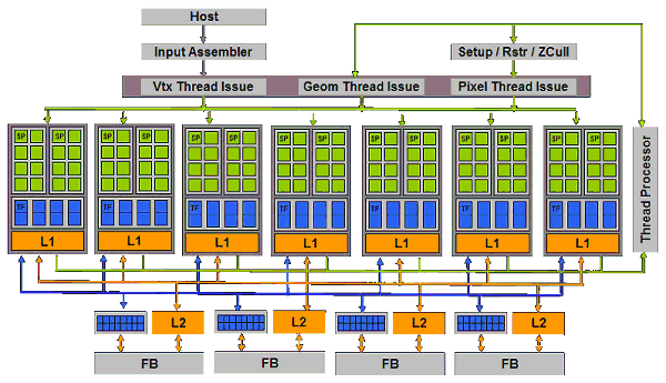 Unified processors and TMUsThe diagram of shader units and evaluation of their peak computing performance in G80 was published in the corresponding article. Nothing has changed for G92, and their performance is easy to recalculate. ALUs in these GPUs operate at more than double frequency. They are scalar units, so they can reach a high efficiency factor. We haven't heard about functional differences yet, whether this GPU offers FP64 or not. There is still support for computations in integer format. They all comply with IEEE 754, which is important for scientific, statistic, economic, and other computations. Texture units in G92 differ from those used in G80. They copy TMUs in G84 and G86, which were modified to increase performance. Each texture unit in G80 could compute four texture addresses and perform eight texture filtering operations per cycle. TMUs in G84/G86 can do twice as many texture lookups. That is each of processors now has eight texture address units (TA) and just as many texture filtering units (TF). 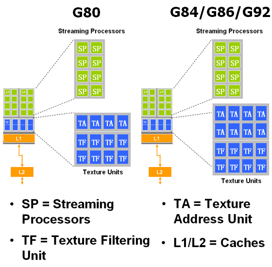 ROPs, frame buffer, antialiasingROPs themselves haven't changed either, but their number has been modified. G80 has six ROPs, and the new solution contains only four of them to reduce manufacturing costs of GPUs and PCBs. This reduction may also have to do with existing High-End solutions, not to fuel competition with them. Each unit processes four pixels (or 16 subpixels). So we've got 16 pixels per cycle for color and Z. Twice as many samples are processed per cycle in Z only mode. The GPU can process two pixels per cycle in MSAA 16x mode, in 4x mode - 8 pixels, etc. Like G80, this GPU supports FP32 and FP16 frame buffers together with antialiasing. A new antialiasing method is supported - Coverage Sampled Antialiasing (CSAA). Another innovation in GeForce 8800 GT is its updated transparency antialiasing. A user had two options: multisampling (TRMS) and supersampling (TRSS). The former was rather fast, but efficient only in few games, and the latter offered high quality but was slow. GeForce 8800 GT is said to offer a new multisampling method for semitransparent surfaces, it demonstrates higher quality and performance. This algorithm improves image quality almost like supersampling, but it's much faster - just a few percents slower than the mode without semitransparent antialiasing. PureVideo HDOne of the long-awaited changes in G92 is its built-in video processor of the second generation, used in G84 and G86, with extended support for PureVideo HD. We already know that these GPUs almost fully offload a CPU, when they decode all types of video data, including H.264 and VC-1. Like in G84/G86, G92 uses a new model of programmable PureVideo HD processor that includes the so called BSP engine. The new processor can decode H.264, VC-1, and MPEG-2 formats with the resolution of up to 1920x1080 and the bitrate of up to 30-40 Mbit/s. It does all the work on decoding CABAC and CAVLC data on the hardware level, so you can play all existing HD-DVD and Blu-ray discs even on mediocre single-core PCs. VC-1 is not decoded as efficiently as H.264, but it's still supported by the new processor. You can read about the second-gen video processor in our article about G84/G86 GPUs. Modern video solutions were partially tested in our latest article about efficiency of hardware-assisted video decoding. PCI Express 2.0One of the real innovations in G92 is its support for PCI Express 2.0. The second version of PCI Express doubles the standard bandwidth from 2.5 Gbps to 5 Gbps. As a result, the x16 slot for graphics cards can transfer up to 8 GB per second in each direction, unlike 4 GB/s provided by PCI Express 1.x. Besides, PCI Express 2.0 is compatible with PCI Express 1.1. Old graphics cards will work with new motherboards, and new graphics cards will still support old motherboards. Provided the external power is sufficient, of course. Besides, you won't enjoy the double bandwidth of the interface. To provide backward compatibility with existing PCI Express 1.0 and 1.1 solutions, Specs 2.0 support both 2.5 Gbps and 5 Gbps modes. Backward compatibility with PCI Express 2.0 allows to use old 2.5 Gbps solutions in 5.0 Gbps slots, which will work at lower speed. Devices compliant with Specs 2.0 support both 2.5 Gbps and 5 Gbps speeds. Theoretically, it all sounds great. But in practice there may be possible compatibility problems with some combinations of motherboards and expansion cards.
Support for external interfacesAs we have expected, the additional NVIO chip in GeForce 8800 cards, which supports external interfaces (2 x 400 MHz RAMDAC, 2 x Dual Link DVI (or LVDS), HDTV-Out), has been integrated into G92. GeForce 8800 GT cards usually come with two Dual Link DVI-I with HDCP support. What concerns HDMI, support for this connector is fully implemented on the hardware level. It can be used by manufacturers in non-reference graphics cards, which may appear a tad later. In fact, a graphics card does not need an HDMI connector, it can be replaced with a DVI-to-HDMI adapter, which is bundled with most modern cards. Unlike RADEON HD 2000 from AMD, GeForce 8800 GT does not contain a built-in audio chip to transfer audio via DVI with the help of an HDMI adapter. This feature is required mostly in Mid- and Low-End cards, which are installed in media centers, so GeForce 8800 GT is hardly an option here. Details: G94, GeForce 9600 SeriesG94 Specifications
Specifications of the Reference GeForce 9600 GT
G94 ArchitectureFrom the architectural point of view, G94 differs from G92 only in quantitative characteristics, it has fewer execution units: ALUs and TMUs. There are not that many differences from G8x either. As we wrote in previous articles, G9x GPUs are actually slightly modified G8x solutions, manufactured by the new fabrication process, with minor architectural changes. The new Mid-End chip has four large shader units (64 ALUs in total) and 32 texture units, as well as four wide ROPs. So, there are not many architectural changes in this GPU, almost all of them have been described above. Everything said about previous solutions remains valid. Here is the main diagram of the G94 GPU: 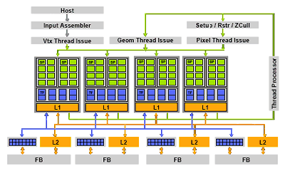 Another advantage of the G9x series and GeForce 9600 GT is a new compression technology implemented in ROPs. According to NVIDIA, it's 15% as efficient as the one used in previous GPUs. They are probably those architectural modifications in G9x for higher efficiency of the 256-bit memory bus versus 320/384-bit solutions we had already mentioned before. The difference will not be that big in real applications, of course. Even NVIDIA states that the performance gain from the new ROPs often amounts to 5%. All these modifications add complexity to the GPU. It comprises quite a lot of transistors. Perhaps, such complexity of the GPU can be explained with the integrated NVIO, a video processor of the new generation, more complex TMUs and ROPs, as well as other hidden modifications: changed cache sizes, etc. PureVideo HDG94 has a built-in video processor of the second generation, used in G84/G86 and G92, with extended support for PureVideo HD. It almost completely offloads a CPU, when the system decodes most popular video formats, including H.264, VC-1, and MPEG-2 with the resolutions up to 1920x1080, 30-40 Mbps. This processor decodes such data fully on the hardware level. Although NVIDIA solutions do not decode VC-1 as efficiently as H.264, and some part of the process still uses CPU resources, you can still play all existing HD-DVD and Blu-ray discs even on mediocre PCs. You can read about the second-gen video processor in our articles about G84/G86 and G92 GPUs. Links to these reviews are published in the beginning of this article. Let's list software improvements in PureVideo HD, which were introduced in GeForce 9600 GT. We can mention double-thread decoding, dynamic contrast/saturation adjustments. These changes did not appear only in GeForce 9600 GT. Starting from ForceWare 174, the new features are introduced into all GPUs supporting PureVideo HD. That list includes such cards as GeForce 8600 GT/GTS, GeForce 8800 GT, and GeForce 8800 GTS 512. Dynamic contrast adjustments are often used in consumer electronics, in TV sets and video players. This feature may improve image quality of video shot with non-optimal cine exposure (a combination of exposure and aperture). That's how it works: when a frame is decoded, the system analyzes its histogram. In case of wrong contrast, the histogram is recalculated and applied to the image. We publish an example below (original image on the left, processed image on the right):  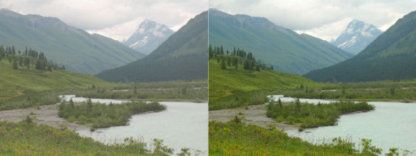 Another useful feature of the latest PureVideo HD is Aero support in Windows Vista during hardware-assisted video playback in a window. This used to be impossible. I cannot say it's a very important feature, but it's still good to have it. Support for external interfacesSupport for external interfaces in GeForce 9600 GT is identical to that in GeForce 8800 GT, except for the integrated DisplayPort support. The additional NVIO chip in GeForce 8800 cards, which supports external interfaces, has been integrated into G92.  Reference GeForce 9600 GT cards come with 2 x Dual Link DVI supporting HDCP. Support for HDMI and DisplayPort is implemented on the hardware level. These ports can be added by manufacturers in non-reference graphics cards. NVIDIA states that unlike G92, support for DisplayPort does not require external transmitters anymore. In fact, a graphics card does not necessarily have to contain HDMI and DisplayPort. They can be replaced with DVI to HDMI/DisplayPort adapters, which are sometimes bundled with modern graphics cards. Reference Information on NV4X Graphics CardsReference Information on G7X Graphics Cards Reference Information on G8X/G9X Graphics Cards Write a comment below. No registration needed!
|
Platform · Video · Multimedia · Mobile · Other || About us & Privacy policy · Twitter · Facebook Copyright © Byrds Research & Publishing, Ltd., 1997–2011. All rights reserved. | ||||||||||||||||||||||||||||||||||||||||||||||||||||||||||||||||||||||||||||||||||||||||||||||||||||||||||||||||||||||||||||||||||||||||||||||||||||||||||||||||||||||||||||||||||||||||||||||||||||||||||||||||||||||||||||||||||||||||||||||||||||||||||||||||||||||||||||||||||||||||||||||||||


