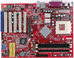
MSI K7N2
(NVIDIA nForce2) Mainboard
|

We tested a preproduction sample, that is why it's quite possible that they
will change it, especially its accessory pack, before throwing the board onto
the market. Accessories: - Package of a standard design;
-
Cables: 2 Serial ATA, 1 ATA66/100/133 and FDD;
- D-Bracket;
-
Bracket for the rear computer panel.

The complains about the board's layout are obvious but not very grave: IDE,
power supply and audio connectors make it difficult to handle the cables inside
the PC case. It can be difficult to reach some jumpers when the board is already
installed. Their functions are shown on the textolite. The 2-channel
switching voltage regulator incorporates 6 capacitors of 2200 uF and 3 of 1500
uF. The following controllers are integrated: - audio controller
based on the chipset's capabilities and C-Media CMI9739A AC'97 codec supporting
5.1 audio systems and having connectors for front audio outputs;
-
network controller based on the chipset's capabilities and supporting 10BaseT/100BaseTX.
Non-unsoldered
connectors: TV-Out (it will probably be available in the model with an integrated
video adapter) and a Serial ATA/IDE RAID controller with connectors. The
system monitoring is supported by the Winbond W83627HF-AW chip. What is controlled:
- processor voltage, +3.3, +-5 and +-12 V, VBAT and +5 V Standby;
-
speed of 2 fans;
- temperatures of the processor (a built-in sensor)
and the board (a built-in sensor).
There are 2 connectors for adjustable
connection of fans. Brief characteristics of the board: memory
slots - 3 DDR SDRAM; expansion slots - AGP/ 5 PCI/ ACR; I/O ports - 2 COM/ LPT/
2 PS/2/ 6 USB 2.0; dimensions - 305x230 mm.

Adjustment
can be carried out with:
| jumpers and switches | Jumper
to clear up the CMOS | | | Jumper for starting
up computer from a PS/2 keyboard | | | Jumpers
for starting up computer from USB keyboard | | | BIOS
based on the AwardBIOS 6.00PG of Phoenix | Setup of memory timings | + | T(RAS),
T(RCD), T(RP), CAS Latency | | Setup of memory frequency | + | FSB:DRAM
= By SPD, 2:1, 5:3, 3:2, 4:3, 5:4, 6:5, 1:1, 5:6, 4:5, 3:4, 2:3, 3:5, 1:2 |
| Setup of AGP bus | - | | | Setup
of PCI bus | - | | | Changeable scaler
of AGP and PCI buses | + | 66-120 MHz in 1MHz steps |
| Manual assignment of interrupts | + | |
| Changeable FSB frequency | + | 100-200 MHz in
1 and 2 MHz steps | | Changeable CPU multiplier | + | x7-x13 |
| Changeable core voltage | + | 1.55-1.8 V in 0.025V
steps | | Changeable memory voltage | + | 2.5,
2.6, 2.7 V | | Changeable chipset voltage | - | |
| Changeable AGP bus voltage | + | 1.5, 1.6, 1.7
V | We used the BIOS 3.0B2 as the latest available version.
It seems that MSI decided that this modern chipset is sufficiently attractive
itself, and there is no need to add frills making it even more expensive. In this
model they stake on the overclocking parameters as well. Test results:
Write a comment below. No registration needed!
|
|

