 |
||
|
||
| ||
|
||
|
||
| ||
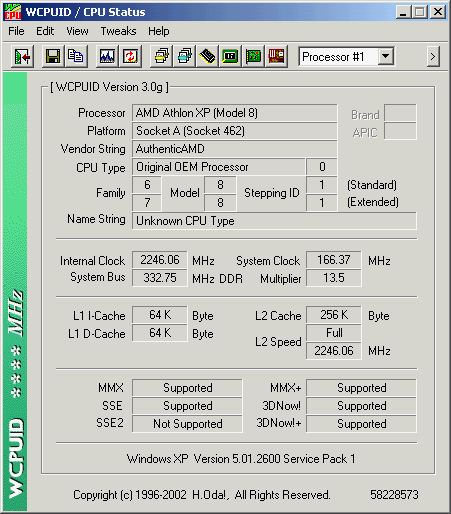
The latest AMD steps can confuse even the experienced PC issue editor, not to mention mere observers. The reason of numerous roadmap changes, announcement delays, and sudden releases is the same — technological problems. I guess that readers, watching our news closely, already know that the AMD has big problems with SOI implementation, and, perhaps, Hammer processors, at least their first samples will be produced in the old fashion. Though, it's hard to estimate wrongs or rights in this situation, as the company tries to atone architectural solution delays by implementing technological solutions, including the transition of Athlon XP (Thoroughbred core, "B" revision (stepping "1")) to 166(333) MHz and the addition of another 256KB L2 cache to die. The new core, combining both novelties, is to be called "Barton", and now AMD announces two Athlon XP models, operating at 166(333) MHz, marked 2700+ and 2800+, according to QuantiSpeed. Athlon XP 2700+ and 2800+Using ratings instead of real clock rates could have complicated the situation even more, but the bus is clearly set between 2700+ and 2600+, so the latter is the last on the older 133 MHz bus. Note that real clock rates at least raise along with ratings, though do not follow a strict formula: 2600+ features 2133 MHz (16x133 MHz), and 2700+ will feature 2167 MHz (13x166 MHz). At that the clock rate difference is lower than that of 133 MHz models, but this is rather fair, as a faster bus surely increases the performance. To examine this boost is the first task of this article. And now let's discuss the announced product itself. Essentially, the transition to a new bus is the official overclocking, possible with the second, more stable core revision release. New processor heating rate is the most interesting here. In general, stepping "1" cores have effective range shifted to higher clock rate area, resulting in 1W higher dissipation of 2000+, for example, but 5W lower dissipation of 2200+. At that all recently announced processors (2400+, 2600+, 2700+ — we still have ïî info on 2800+) dissipate same (max./typical) heat 68.3/62W at the same core parameters (1.65V supply voltage, 85°C max die temperature). The heat is almost identical to 2200+ parameters at the moment of release (stepping "0"). Therefore, system requirements remain the same, including certified copper-base cooler. Though we have a chance to demonstrate 2800+ performance, this processor is not shipped yet, and will not be in mass production till Christmas at least, and by that time Barton is ought to be released, featuring similar clock rates, and, besides, increasing L2 cache up to 512KB won't result in significant rating increase. Thus let's wait for news and definiteness from AMD, and for now just introduce photos of the tested sample. 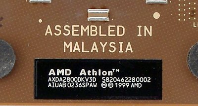
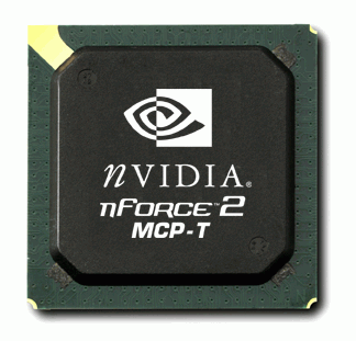
 NVIDIA nForce2It turned out to be so that we've got the first nForce2 board sample simultaneously with AMD new CPU, so we couldn't disclose all nForce2 details and advantages in this time-limited testing. In the nearest future we'll do this for sure, trying to describe all interesting features. And the current ASUS A7N8X testing is a good reason to introduce NVIDIA nForce2 to our readers. First, the novelty isn't that revolutionary, but the evolved chipset is far feature-richer than competing products. The most interesting and pleasant is that this time NVIDIA plans to take over a significant market share, reasonably staking on the discrete chipset variant, promising to keep its price up to $10 higher than that of competing products (i.e. VIA KT333/KT400). But let's discuss it in order. nForce2, similar to its nForce predecessor, features 4 variants at the moment of announcement, made of various North- and Southbridge bundles. Still there's a principal difference: no announcements on pared-down nForce 220 (with a single-channel memory controller) let NVIDIA understand the hopelessness of such policy, so nForce2 Northbridge has only one, high-performance variant. But the discrete variant (w/o integrated graphics), rather popular among mobo makers in case of nForce, has not only been provided from the very beginning, but will also be shipped first. Clearly, NVIDIA considers the new chipset not a graphics product ad, but a fully-featured standalone product. So, to provide the specifications. NVIDIA nForce2 bases on the classic dual-bridge design (still NVIDIA prefers the word "processors" to underline the significant work they perform, offloading CPU). Northbridge has two variants: nForce2 IGP (Integrated Graphics Processor) and nForce2 SPP (System Platform Processor w/o graphics). Southbridge has two variants as well: MCP (Media and Communication Processor) and MCP-T (we couldn't understand what does "T" mean :)). Their significant difference is described further. 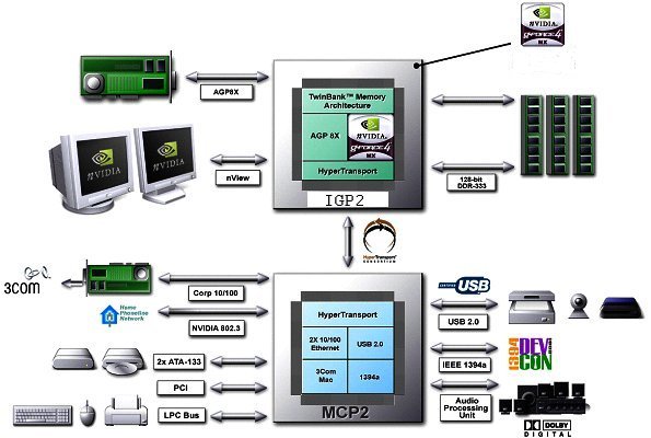 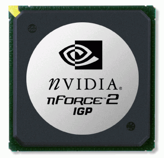
IGP graphics core is actually similar to GeForce4 MX GPU, fully described in the "Video" section. Note one main difference: IGP naturally doesn't have own graphics memory, and system SMA memory, operates at significantly lower clock rate than that of NVIDIA GeForce4 MX 440 with AGP8x (based on the same NV18). Moreover, only at maximum 200(400) MHz (DDR400) supported memory clock rate integrated graphics core reaches the level of older NVIDIA GeForce4 MX 440. In the future reviews we'll check how theoretical performance of integrated graphics corresponds to the actual, and now let's pause at IGP features non-gaming. The most important are: nView (dual-monitor output), DVI interface, integrated TV-Out and fully hardware DVD/MPEG2 encoding. All the details are provided in the "Video" section, and we proceed to the remaining Northbridge-related part. Again, it's not that revolutionary, but features very many minor advantages. So, the chipset supports any Socket A CPUs with 100(200), 133(266) and 166(333) MHz FSB. Unofficially it also supports 200(400) MHz FSB (to note and continue with the features). The chipset can work with up to 3GB DDR200, DDR266, DDR333, DDR400 memory (remember, the latter is unofficial as well) and provides (even IGP) AGP 4x/8x functionality. These are almost standard features of a current Northbridge, but NVIDIA has a couple of trumps. The first is the undoubtedly smart transaction coordinator. Fine-tuned buffering and prefetch system (DASP) is used to control vast data transfers between CPU, memory, GPU, and Southbridge. We've already examined its functionality in detail in the same NVIDIA nForce preview. The second DASP generation, according to NVIDIA, provides more aggressive algorithms. Pity, we have no more details about improvements, but considering the first nForce test results, we can state that the performance of such complex mechanisms should be tested in the field. Note that NVIDIA engineers faced a really difficult task, as the data stream distribution should be performed even at fully asynchronous bus operation (at that independent CPU bus, memory, or AGP clock rate change is also possible). The second unique technology, used by NVIDIA to top the chipsets, is called "DualDDR" (readers of nForce review know it as "TwinBank"). If short, the idea is to use two 64-bit memory controllers, distributing tasks in such a way to provide alternate controller operation for 128-bit memory access and theoretically twice lower latencies. Again, all the details are provided in the NVIDIA nForce preview. Just note that DualDDR Memory Architecture features one more address bus (with the total of three, given two data buses), providing fast access and maximum clock rate to all three memory modules supported. Another thing is the capability of using up to three DIMMs of any organization and performance, though one have to use similar modules in "0" and "1" sockets for the maximum performance. Finally, remember that in NVIDIA product lines Northbridge is connected to
the South bridge via 800 MB/sec HyperTransport bus. And if this was too much for
nForce, the second chipset generation might use all 100% of it. Proceeding to MCP specs (fully-featured MCP-T first), we'd like to state that we won't describe networking and audio capabilities here. All necessary tests are the subject of time. Now let's just mention the main components, that NVIDIA stuffed the Southbridge with. In addition to the LAN controller, the new-generation chipset feature 3Com's MAC — this is called DualNet. Both utilize the proprietary isochronous StreamThru technology for delivering data to the Northbridge. According to NVIDIA, it provides some performance boost, comparing to usual PCI transfer analogs. Audio is represented by 2/4/6-channek codec or a pair of codecs and already familiar nForce APU with Dolby Digital 5.1 encoding support (called SoundStorm) or without it. As for the peripheral interface support, NVIDIA provided USB 2.0 integrated controllers (single EHCI, up to 6 ports) and Firewire(IEEE1394a). Naturally, hard disk interface is provided as well, but it's only average part of the chipset, featuring usual ATA133 IDE controllers instead of SerialATA. It's strange, because NVIDIA have taught us to expect original solutions only. :) If you are tired of pluses, let's mention minuses or what's absent in the simpler and cheaper MCP variant. The networking connectivity is pared down to original MAC, audio features a codec only, no Firewire support provided. Though the remaining is good as a current fully-featured Southbridge, and if motherboards, based on this budget version, will actually be budget, we can certainly forecast the bright future. Finishing the chipset description, we provide the list of its trade titles, mentally thanking NVIDIA for omitting all senseless, but confusing numbers: now "G" means the presence of integrated graphics core, "S" — its absence. MCP-T Southbridge surely adds "T". Now you can position "nForce2-GT", "nForce2-G", "nForce2-ST", and "nForce2-S" by yourself. In addition, introducing photos of bridge markings of ASUS A7N8X sample, based on IGP and MCP-T: 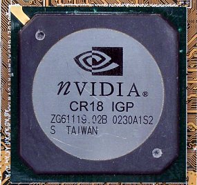
 Performance testingTestbed:
Software:
Brief comparative specifications of motherboards tested:
Before testing we conducted a quick compatibility check. ALi MAGiK 1 C is the first (chronologically) with the announced 166(333) MHz FSB support. Naturally, the future or overclocked, as that time even AMD didn't plan to speed up Athlon XP like that. The only such board, occasional in our lab, couldn't boot with installed Athlon XP 2800+. Older SiS735 specification didn't mention 166(333) MHz FSB support, but it was worth a try. Pity, we haven't had newer SiS chipset boards yet. So, we had almost no choice, and nForce2 was to compete with VIA product. We decided to use KT400, as newer and more interesting, and kind of capable of 200(400) MHz memory interaction (now, when JEDEC gives no hope of standardizing DDR400, chipset makers lay off DDR400 operability problem to mobo makers). Initially, we wanted to compare the performance using PC3200, but only KT400 was capable to work in such conditions, besides, only in synchronous mode, like DDR333 (so we were limited by DDR333 in all KT400 tests). Moreover, the express test, which results are not provided here, showed that nForce2 always worked slightly faster using CPU-synchronous clock rate, despite claims special DDR400 optimizations. So, we were unable to test anything with DDR400.
Enough lyricism, let's get back to testing. What was it interesting to test, having a sample of CPU with a new bus? Naturally, to compare it with older-bus model. Though, it's impossible, as older and newer lines feature different clock rates. So, without a technical opportunity to change CPU multiplier, we were forced to indirect comparison, using the same CPU working with 133(266) MHz FSB. Comparing the results with CPU scale multiplier of each test app, we could estimate the boost, provided by a faster bus. Comparing performance results of systems, based on two different chipset (KT400 (actually as KT333) against nForce2), we could also estimate the effect of the still unbeaten (among DDR chipsets) NVIDIA dual memory controller subject to CPU FSB clock rate. Finally, diagrams were also stuffed with 2.8 GHz Pentium 4 results, but I must say that this fight is virtual only: Athlon XP 2800+ is not available on the market (like all its recently announced siblings from 2400+), and moreover, no one can even promise that it will have mentioned parameters at the moment of release. Test resultsCPU RightMark hasn't surprised us: the performance of the same-architecture
systems almost completely depends on CPU clock rate and cache performance. Variations
do not exceed the extent of error. And the relative position of AMD and Intel
CPUs is rather usual and commented. Low-level memory interaction performance is more interesting: omitting Rambus
walkaway, pay attention to KT400 slight superiority with 133 MHz FSB (yet PC2700
was faster than nForce2 memory, operating as PC2100). It stresses the sudden burst
of NVIDIA's dual-channel controller after transition to 166 MHz FSB and memory
clock rate, keeping pace. Note that nForce2 walkaway the competitor, using DASP prefetch, in well-predictable
Wstream. MP3 encoding is a calculating task, so identical results of same-rated CPUs
and different chipsets and almost 100% test scaling with Athlon XP do not surprise.
But MPEG4 encoding is another thing: the performance here is estimated by CPU
pushing data through memory. Here faster FSB provides a very nice boost — 100%
scaling on nForce2. Even rather good 70% of KT400/KT333 look pale on this background.
The conclusion is simple: using new Athlon XP on VIA chipsets, encoding performance
is limited by memory access, though providing a significant boost. DDR400 should
provide noticeable effect here. if it's possible at all, of course. But in case
of nForce2 CPU overclocking is not limited, and any further model will work proportionally
faster. Pentium 4 wins in this test mainly due to SSE2 support, that's rather
far from today's theme. Using both archivers resembles MPEG4 encoding much. Larger dictionaries chain
these tests to CPU-memory performance, and here nForce2 almost doesn't limit processor
requirements (80-90% scalability), but VIA chipset provides only a boost (30-40%).
The slight difference is that WinAce showed similar results for both competitors,
and WinRAR made Pentium 4 the leader. 3ds max rendering usually requires CPU clock rate, so remembering the approximate
equality of Athlon XP 2600+ and Intel Pentium 4 2.8 GHz (ascertained in our recent
comparison), do not be surprised that the higher clock rate model wins. Games, requiring another throughput-greedy component — graphics card, show already familiar situation. Naturally, there were no surprises in hi-res modes, where graphics cards slow down, still 60% boost was rather significant. And lower resolutions at lower scene detail chain system performance to CPU and memory, again showing almost 100% scalability with nForce2. ConclusionsThey will be brief, as all comments are already provided in the article. We've proved a rather obvious empirical guess that Athlon XP system performance is limited to FSB throughput since DDR333 chipsets release. We've also proved another obvious guess that DDR333 throughput is not enough for similar FSB (same with VIA KT266/A, when KT333 noticeably sped up 266 MHz CPUs). NVIDIA nForce2 showed itself very nice, that, considering its functionality, makes it the best buy, especially for recently announced and future AMD CPUs (this idyll might be spoiled only by high prices). Finally, we can state that in the most apps Thunderbird P-rating of AMD Athlon XP could have wondrously almost coincide with the corresponding Pentium 4 rating, being it ever introduced. Write a comment below. No registration needed!
|
Platform · Video · Multimedia · Mobile · Other || About us & Privacy policy · Twitter · Facebook Copyright © Byrds Research & Publishing, Ltd., 1997–2011. All rights reserved. | ||||||||||||||||||||||||||||||||||||||||||||||||||||||||||||||||||||||||||||||||||||||||||||||||||||||


