The next release of the universal benchmark package RightMark Memory Analyzer for low-level
platform testing contains, in the first place, a range of new informational
features. The new version of the benchmark provides even more detailed
reference information about the platform, this trend started in Version 3.0. For a start the developers implemented
extraction of information about the most important platform component
- CPU, by decoding values returned by the CPUID instruction. The logical
continuation of the info section development would have been data
mining for the two remaining platform components - chipset and RAM.
And this is exactly what has been implemented - discover the new features!
Platform Information
You are already familiar with the chipset information provided by
RMMA - refer to the description of Version 3.0 for details. Little has changed in
the new version of the benchmark - it still features a chipset database
provided with the program, which offers such information (unavailable
in CPUID) as latency of the access to the cache level, bus width and
its hierarchy. So let's proceed to the Chipset tab.
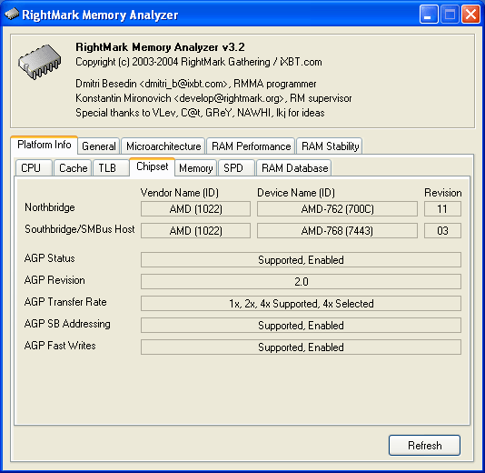
The title speaks for itself: chipset information. This tab displays
the names and IDs of the vendor, device, and the revisions of Northbridge
and Southbridge (namely its SMBus controller - we shall give the reason
later). It also displays information about the AGP-controller, for
completeness sake. To be fair though it should be noted that in the
light of new Intel 915/925 chipsets in
future this information may be losing its actuality. However nothing
prevents the developers to update it or add information on the PCI Express controller.
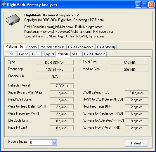
The next tabbed page (Memory) contains almost everything you
need to know about the memory installed in the system. Note that this
is the maximum complete data provided by the memory controller,
which is usually located in the northbridge of the chipset (or in the
CPU itself, in case of the AMD K8 family; but note, that from the configuration
point of view such a controller is the same "virtual" PCI-device as
a common memory controller in the northbridge). The most important parameters
- the type and size of the installed memory, its bus frequency (availability
of this parameter depends on the availability of data on a CPU multiplier
and the DRAM:FSB frequency ratio) and, of course, its current
timings. Note that various chipsets provide different sets with often
incomplete memory timing parameters, so the example on the screenshot
is sort of ideal - but in fact it's real (for those who are interested,
it is taken with a relatively exotic AMD 760MPX chipset). Below is a
list of the most important memory timings, commonly used in memory reviews,
listed in order of their importance:
- CAS# Latency, tCL
- RAS# to CAS#
Delay, tRCD
- Row Precharge, tRP
- Activate to Precharge or
RAS# Active Time, tRAS
Thus, in our example a RAM module will be characterized by the 2.0-2-2-6
timing scheme. And finally, you can choose a Module Index
of one of the four modules (from 0 to 3) in the bottom of the screen.
It should be noted that most modern chipsets have common memory timing
settings for all modules, though you may come across samples with
separate timings for each module (usually in chipsets supporting more
than one memory type).

The last of the info tabs - SPD data (Serial Presence Detect chips)
of the selected memory module (its number specified like on the previous
tab - by selecting a Module Index from 0 to 3). The
information is read from the memory module SPD chip via I2C-compatible
SMBus transport protocol using registers of the SMBus controller (IO
ports) in the southbridge of the chipset. SMBus controller is usually
implemented as a self-contained "virtual" PCI-device, and thus the
Chipset section described above contains the ID of
this device. Let's return to the SPD data. As in the previous tab,
the most important parameters are the type, size, module frequency,
and the timings recommended by the manufacturer, usually labeled "by
SPD" in BIOS settings. It's significant to note that many memory
modules can have more than one timing type specified. They differ
by CAS# Latency, tCL and by Cycle
Time, tCK. In order to display all possible timings,
the bottom part of the tabbed page contains a drop-down list, where
you can select one of the three timing indices:
- CLX: Timing value at the maximum value of the supported CAS# Latency (tCL). So,
if the table of the supported DDR
SDRAM CAS# Latency values contains 2.0, 2.5, 3.0, CLX timings correspond to the case tCL = 3.0;
- CLX-1: Timing value at the maximum value of the supported CAS# Latency (tCL) minus one
cycle (for SDRAM and
DDR2 SDRAM memory types) or a half cycle (for DDR SDRAM). In our example CLX-1 corresponds to the timings at tCL = 3.0 - 0.5 = 2.5;
- CLX-2: Timing value at the maximum value of the supported CAS# Latency (tCL) minus two cycles
(for SDRAM and DDR2 SDRAM memory types) or one cycle (for DDR SDRAM). In our example CLX-2 will correspond to the timings at tCL = 3.0 - 1.0 = 2.0.
This tabbed page also provides information about the error correction type (Correction,
options: None, Parity, ECC), module attributes (Attributes,
options: None, Buffered, Registered), its Manufacturer, and Part Number. It should be noted that noname manufacturers (as you can see in the screenshot)
not always provide such data in the SPD
module chip.
RAM Database
The last tab in the Platform Info section is not directly connected with platform info, but it's an important part of the new version of RMMA.
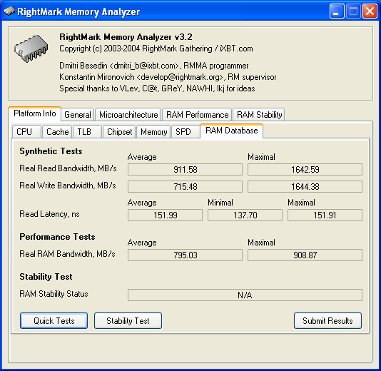
It is interesting in two respects. First of all, it allows inexperienced
users to measure the most important characteristics of the memory
subsystem quickly and without any hassle - namely, its real bandwidth
(in synthetic ("measuring") as well as real ("competitive")
benchmarks) and latency. This is done at a single click on the Quick
Tests button, the benchmarks taking, depending on the memory
subsystem performance, just a couple of minutes. Benchmark results
include average parameters, taken without any optimization, as well
as the best ones (in case of a maximum CPU bus bandwidth) by all optimization
options for reading from memory/writing to memory.
Besides, if you wish, you can run another test -
memory test for operation stability at this configuration
(with the current timings). This test takes quite much time (60 minutes), so, when you run this test, the program pops up a warning and you can cancel the test. You can also cancel the test while it is already running, but in this case its results are not taken into consideration.
The second feature offered by this tab is an opportunity to contribute to the development of our database (catalog) of memory modules, which is presently in the early stage of development. You can do it by clicking the Submit Results button. In this case, if the Quick Tests were successfully completed, the program opens the following dialog window.
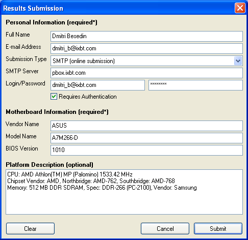
Settings are clear: information about a user (full name and an e-mail
address for confirmations about the reception of the results and their
submittal to the database after moderatorial approve), which is, for
convenience sake, stored in a configuration file (rmma.ini).
Besides, for now users will have to type information about their mainboards
manually - Vendor Name, Model Name
and BIOS Version fields (later,
these parameters will be detected automatically via Desktop Management
Interface, DMI). We urge our users to treat this procedure with maximum
caution, because it directly concerns the value of the submitted results.
Besides, volunteers may provide any additional (but not mandatory)
information about the platform (up to 255 symbols), which may prove
useful for our database. The memory database is planned to contain
the following information:
- CPU (CPUID results, clock frequency, quantity of system processors).
- Mainboard (manufacturer, model, BIOS), link to the mainboard description.
- Chipset (manufacturer, device ID, revision, etc.), link to the
chipset description.
- Current memory timings.
- SPD for all memory modules, including the manufacturer, Part Number,
organization, module attributes, recommended timings.
- Memory module specifications from vendor, link to vendor's web
site.
- Photo of the memory module.
- Photo of the memory chip.
- Results of the memory stability tests for this mainboard and chipset
at the specified timings.
- Measuring results of the real CPU bus bandwidth and memory latency
for this mainboard and chipset at the specified timings.
Besides, it is planned to implement results sorting - searching
for modules with the best timings for a selected mainboard and vice
versa.
Currently implemented ways to submit results include a so called offline submission (in this case the results are saved to a file named after user's e-mail address,
then the user manually e-mails this file as attachment at the database address provided in the program) and an online SMTP submission (in this case test results stored in a file are automatically sent at the database address, and then the program confirms the completion of the operation). In future it is planned to implement an online-submittal via HTTP and an automatic reception of the test results by the HTTP-server hosting the RightMark project database.
Write a comment below. No registration needed!


