 |
||
|
||
| ||
|
||
|
||
| ||
We proceed with a new series of articles devoted to the low level analysis of the most important characteristics of memory modules using our RightMark Memory Analyzer universal test package. I remind you that the purpose of this analysis is to provide all interested readers with information on compatibility of a given memory module from a given manufacturer with different mainboards based on various chipsets. Today the object of our analysis is 512-Mb DDR2-modules Kingston ValueRAM. Manufacturer Information
Module manufacturer: Kingston Technology Module AppearancePhoto of the memory module Photo of the memory chip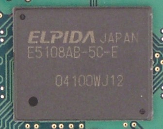 Part Numbering System of Modules and Chips Module Part Number Expansion
Description of the part numbering system of DDR2 Kingston ValueRAM modules: http://www.kingston.com/literature/MKF_586.pdf
Chip Part Number Expansion
Data sheet on 512 Mbit DDR2 Elpida memory chips: http://www.elpida.com/pdfs/E0323E81.pdf
Note that part numbering of this module, to put it mildly, is different from the official specification provided in the data sheet on this memory chip type. Namely, there are no fields with the device type (monolithic, DDR2) and package (FBGA). Perhaps, it has something to do with the fact that the memory module we got is not a production but an engineering sample. And it most likely uses an earlier revision of Elpida memory chips than the one described in the data sheet. SPD module chip data
Description of the SPD general standard:
Description of the SPD specific standard for DDR2:
According to the SPD chip data, this module has the 64M x 64 organization type and can operate at three different CAS latencies (tCL) of 5, 4 and 3. It's interesting to note that the first two values of tCL, CL X = 5 and CL X-1 = 4, correspond to the same 3.75 ns clock cycle, that is operating in normal DDR2-533 mode at 266.7 MHz. In this case module timings can be written as 5-4-4-12 and 4-4-4-12 correspondingly. The last supported CAS latency value (CL X-2 = 3) corresponds to the 5.00 ns clock cycle, that is operating at 200.0 MHz in DDR2-400 mode. The corresponding timings are 3-3-3-9. Another distinctive feature of this module is a relatively large minimum refresh to active/refresh command period (tRFC) – 105 ns, which corresponds to 28 memory bus cycles at 266.7 MHz and 21 cycles at 200.0 MHz. Testbed Configurations and SoftwareMainboards based on the chipsets of Intel 915 seriesTestbed #1
Testbed #2
Testbed #3
Testbed #4
Testbed #5
Testbed #6
Mainboards based on the chipsets of Intel 925 seriesTestbed #7
Testbed #8
Testbed #9
Testbed #10
Testbed #11
Test ResultsMainboards based on the chipsets of Intel 915 seriesFrom this time on, memory modules will be tested in two modes. The first series of tests – let's call them "performance tests" – are carried out in normal mode, that is with standard timings written in the SPD chip. The second series of tests is carried out in so called "extreme" mode with maximum possible timings for a given module on a given mainboard. Let's call this test series "stability tests", because the capacity to operate steadily with "harder" timings for a long time can be directly associated with operating stability in normal mode. Performance testsDDR2 Kingston modules in DDR2-533 mode suppose the existence of two different timing schemes, 5-4-4-12 and 4-4-4-12. But in the first series of tests we used the 4-4-4-12 scheme, because, firstly, it is closer to values typical of DDR2-533, and, secondly, it was set in BIOS settings by default (Memory Timings: "by SPD") in all mainboards unexceptionally. As we have already mentioned before, the current generation of processors and chipsets with the FSB frequency of 800 MHz does not allow to reach the maximum DDR2-533 throughput in dual channel mode. Nevertheless, even in this case we can draw certain conclusions about the real memory bandwidth, which can be achieved on various mainboards. |
| Parameter* | Testbed 1 | Testbed 2 | Testbed 3 | Testbed 4 | Testbed 5 | Testbed 6 |
| Timings |
|
|
|
|
|
|
| Average memory read bandwidth, MB/sec |
|
|
|
|
|
|
| Average memory write bandwidth, MB/sec |
|
|
|
|
|
|
| Max. memory read bandwidth, MB/sec |
|
|
|
|
|
|
| Max. memory write bandwidth, MB/sec |
|
|
|
|
|
|
| Minimum Pseudo-Random Access Latency, ns** |
|
|
|
|
|
|
| Maximum Pseudo-Random Access Latency, ns** |
|
|
|
|
|
|
| Minimum Random Access Latency, ns** |
|
|
|
|
|
|
| Maximum Random Access Latency, ns** |
|
|
|
|
|
|
*the best results are in bold
**Block size – 16 MB
MSI 915P Neo2 based on i915P (Testbed #4) is the leader almost by all parameters (maximum real memory bandwidth, minimum memory latency) among the mainboards based on Intel 915P/915G. Interestingly, it's actually the only leader – all the other mainboards, regardless of the chipset type (P/G), have demonstrated more or less average results. So, the values of real read memory bandwidth are within 4470-4480 MB/sec, maximum memory bandwidth – within 6330-6350 MB/sec, the pseudo-random access latency is within 55-64 ns. By the way, the first place of MSI 915P Neo2 can be comparatively easy explained by its somewhat increased FSB frequency. It results in the increase of maximum real write memory bandwidth to 4324 MB/sec, which is normally limited to the 2/3 of the system bus throughput (4266.7 MB/sec).
Before we proceed to quantitative evaluation of memory bandwidth/latency in the "extreme" mode, let's dwell on memory timings proper, which values were varying "on the run" due to the built-in RMMA function to dynamically modify memory settings supported by the chipset. Memory system stability with certain timings was estimated using a specially developed utility, which will be included into the next RMMA version as an add-on to the existing RAM Stability Test.
So, minimal timings allowed in DDR2 Kingston modules are 4-3-3-8. The memory system is quite stable in this mode on most mainboards used in this test, except for "combined" boards based on i915G supporting both DDR and DDR2 simultaneously – MSI 915G Combo (Testbed #5) and ASUS P5GDC-V (Testbed #6). Minimal timings allowed on these mainboards without compromising the operating stability of the memory system are 4-3-3-9.
| Parameter* | Testbed 1 | Testbed 2 | Testbed 3 | Testbed 4 | Testbed 5 | Testbed 6 |
| Timings |
|
|
|
|
|
|
| Average memory read bandwidth, MB/sec |
|
|
|
|
|
|
| Average memory write bandwidth, MB/sec |
|
|
|
|
|
|
| Max. memory read bandwidth, MB/sec |
|
|
|
|
|
|
| Max. memory write bandwidth, MB/sec |
|
|
|
|
|
|
| Minimum Pseudo-Random Access Latency, ns** |
|
|
|
|
|
|
| Maximum Pseudo-Random Access Latency, ns** |
|
|
|
|
|
|
| Minimum Random Access Latency, ns** |
|
|
|
|
|
|
| Maximum Random Access Latency, ns** |
|
|
|
|
|
|
*the best results are in bold
**Block size – 16 MB
You can easily see that the use of a "harder" timing scheme does not change the overall picture of the memory performance, which we got in the previous series of tests. MSI 915P Neo2 (Testbed #4) is still a leader, while all the other mainboards demonstrate approximately the same results.
As in our previous tests,
on the whole, mainboards based on i925X outscore the mainboards based
on i915P/i915G by all parameters. The leader in this series is again
a mainboard from MSI – 925X Neo (Testbed #10), which is also
achieved by a slightly higher FSB frequency (maximum real memory write
bandwidth – 4327 MB/sec). The second place, almost with the
same result, is shared by Gigabyte 8ANDXP-D (Testbed #7), ASUS P5AD2
(Testbed #9) and Foxconn 925A01-8EKRS (Testbed #11). Intel D925XCV
(Testbed #8) is the last almost by all parameters.
| Parameter* | Testbed 7 | Testbed 8 | Testbed 9 | Testbed 10 | Testbed 11 |
| Timings |
|
|
|
|
|
| Average memory read bandwidth, MB/sec |
|
|
|
|
|
| Average memory write bandwidth, MB/sec |
|
|
|
|
|
| Max. memory read bandwidth, MB/sec |
|
|
|
|
|
| Max. memory write bandwidth, MB/sec |
|
|
|
|
|
| Minimum Pseudo-Random Access Latency, ns** |
|
|
|
|
|
| Maximum Pseudo-Random Access Latency, ns** |
|
|
|
|
|
| Minimum Random Access Latency, ns** |
|
|
|
|
|
| Maximum Random Access Latency, ns** |
|
|
|
|
|
*the best results are in bold
**Block size – 16 MB
Unlike the first series of tests with mainboards based on i915P/i915G, all tested mainboards based on i925X are doing fine with DDR2 Kingston modules with minimal timings of 4-3-3-8.
| Parameter* | Testbed 7 | Testbed 8 | Testbed 9 | Testbed 10 | Testbed 11 |
| Timings |
|
|
|
|
|
| Average memory read bandwidth, MB/sec |
|
|
|
|
|
| Average memory write bandwidth, MB/sec |
|
|
|
|
|
| Max. memory read bandwidth, MB/sec |
|
|
|
|
|
| Max. memory write bandwidth, MB/sec |
|
|
|
|
|
| Minimum Pseudo-Random Access Latency, ns** |
|
|
|
|
|
| Maximum Pseudo-Random Access Latency, ns** |
|
|
|
|
|
| Minimum Random Access Latency, ns** |
|
|
|
|
|
| Maximum Random Access Latency, ns** |
|
|
|
|
|
*the best results are in bold
**Block size – 16 MB
And again the use of a "harder" timing scheme did not lead to any considerable changes in the alignment of forces. The first place is taken by MSI 925X Neo, the second place is shared by Gigabyte 8ANDXP-D and ASUS P5AD2, while Foxconn 925A01-8EKRS is a tad behind them taking the third place. Well, and Intel D925XCV is the last in this series of tests.
Thus, the best memory system performance with DDR2 Kingston ValueRAM modules is achieved on the mainboards based on Intel 925X, especially on MSI 925X Neo. Among the mainboards based on Intel 915P/915G, the best performance is also demonstrated by a mainboard from MSI – 915P Neo2. The worst performance of the memory system (among the counterparts) is demonstrated by the mainboards from Intel – D925XCV and D915GUX. What concerns operating stability of the memory system (in "hard" mode), all tested mainboards demonstrate similar results, except for "combined" models supporting both DDR and DDR2 simultaneously – MSI 915G Combo and ASUS P5GDC-V.
Write a comment below. No registration needed!
|
Article navigation: |
| blog comments powered by Disqus |
| Most Popular Reviews | More RSS |
 |
Comparing old, cheap solutions from AMD with new, budget offerings from Intel.
February 1, 2013 · Processor Roundups |
 |
Inno3D GeForce GTX 670 iChill, Inno3D GeForce GTX 660 Ti Graphics Cards A couple of mid-range adapters with original cooling systems.
January 30, 2013 · Video cards: NVIDIA GPUs |
 |
Creative Sound Blaster X-Fi Surround 5.1 An external X-Fi solution in tests.
September 9, 2008 · Sound Cards |
 |
The first worthwhile Piledriver CPU.
September 11, 2012 · Processors: AMD |
 |
Consumed Power, Energy Consumption: Ivy Bridge vs. Sandy Bridge Trying out the new method.
September 18, 2012 · Processors: Intel |
| Latest Reviews | More RSS |
 |
Retested all graphics cards with the new drivers.
Oct 18, 2013 · 3Digests
|
|
Added new benchmarks: BioShock Infinite and Metro: Last Light.
Sep 06, 2013 · 3Digests
|
|
Added the test results of NVIDIA GeForce GTX 760 and AMD Radeon HD 7730.
Aug 05, 2013 · 3Digests
|
 |
Gainward GeForce GTX 650 Ti BOOST 2GB Golden Sample Graphics Card An excellent hybrid of GeForce GTX 650 Ti and GeForce GTX 660.
Jun 24, 2013 · Video cards: NVIDIA GPUs
|
|
Added the test results of NVIDIA GeForce GTX 770/780.
Jun 03, 2013 · 3Digests
|
| Latest News | More RSS |
Platform · Video · Multimedia · Mobile · Other || About us & Privacy policy · Twitter · Facebook
Copyright © Byrds Research & Publishing, Ltd., 1997–2011. All rights reserved.


