Memory Module Analysis. Part 3: Kingston DDR-533 Modules
|
We proceed with the series of articles, dedicated to the low level analysis
of the most important characteristics of memory modules using our
RightMark Memory Analyzer
test package. The object of today's review is a couple of Kingston
DDR-533 modules, high performance HyperX series for overclockers.
Manufacturer Information
Module manufacturer: Kingston Technology
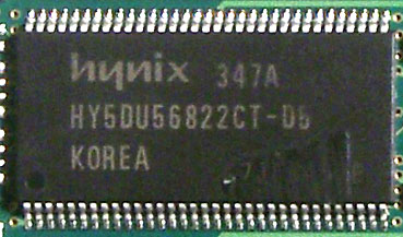
Manufacturer of module chips: Hynix Semiconductor
Web site of the module manufacturer: http://www.kingston.com/hyperx/products/khx.asp
Web site of the chip manufacturer:
http://www.hynix.com/eng/02_products/01_dram/index.jsp
Module Exterior
Photo of the memory module
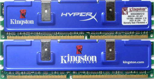
Photo of the memory chip
Module and Chip Part Number
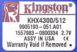
Module Part Number Expansion
Data sheet on Kingston HyperX DDR-533 modules does not contain the expansion of some Part Number components. The documentation provides only brief technical characteristics of the module.
| Field |
Value |
Expansion |
| 0 |
KHX4300/512 |
Module density: 512 MB
Module organization: 64M x64
Voltage: Vdd: 2.7(+/-)0.1V, Vddq: 2.7(+/-)0.1V
Timings (tCL-tRCD-tRP-tRAS): 3-4-4-8 |
Chip Part Number Expansion
Description of the part numbering system of Hynix memory chips:
http://www.hynix.com/eng/02_products/01_dram/down/DDR.pdf
| Field |
Value |
Expansion |
| 0-1 |
HY |
Manufacturer code: HY = Hynix Memory |
| 2-3 |
5D |
Product family: 5D = DDR SDRAM |
| 4 |
U |
Process technology/voltage: U = VDD 2.5V, VDDQ 2.5V |
| 5-6 |
56 |
Capacity and refresh: 56 = 256M, 8K refresh |
| 7-8 |
8 |
Organization: 8 = x8 |
| 9 |
2 |
Number of banks: 2 |
| 10 |
2 |
Interface: 2 = SSTL_2 |
| 11 |
C |
Chip generation C = 4th generation |
| 12 |
|
Power Consumption: (blank) = normal |
| 13 |
T |
Package type T = TSOP |
| 14 |
|
Die package type (blank) = a single die |
| 15 |
|
Package material: (blank) = usual |
| 16 |
— |
(blank) |
| 17-18 |
D5 |
Speed/Timings: D5 = DDR500, 3-4-4 |
| 19 |
|
Temperature conditions: (blank) = usual (0 — 70°C) |
According to the expansion of the chip designation, these modules use DDR-500 chips, designed for 3-4-4 timings. However, the DDR-533 value in the Part Number expansion table of Hynix memory chips is not provided.
SPD module chip data
Description of the general SPD standard:
JEDEC Standard No. 21-C, 4.1.2 - SERIAL PRESENCE DETECT STANDARD, General Standard
Description of the specific SPD standard for DDR:
JEDEC Standard No. 21-C, 4.1.2.4 — Appendix D, Rev. 1.0: SPD’s for DDR SDRAM
| Parameter |
Byte |
Value |
Expansion |
| Fundamental Memory Type |
2 |
07h |
DDR SDRAM |
| Number of Row Addresses on this assembly |
3 |
0Dh |
13 (RA0-RA12) |
| Number of Column Addresses on this assembly |
4 |
0Ah |
10 (CA0-CA9) |
| Number of DIMM Banks |
5 |
02h |
2 physical banks |
| Data Width of this assembly |
6, 7 |
40h, 00h |
64 bit |
| Voltage Interface Level of this assembly |
8 |
04h |
SSTL 2.5V |
| SDRAM Cycle time (tCK) at maximum supported CAS# latency (CL X) |
9 |
50h |
5.00 ns (200.0 MHz) |
| DIMM configuration type |
11 |
00h |
Non-ECC |
| Refresh Rate/Type |
12 |
82h |
7.8125 ms — 0.5x reduced self-refresh |
| Primary SDRAM Width (organization type) of the memory module chips |
13 |
08h |
x8 |
| Error Checking SDRAM Width (organization type) of the memory chips in the ECC module |
14 |
00h |
Not defined |
| Burst Lengths Supported (BL) |
16 |
0Eh |
BL = 2, 4, 8 |
| Number of Banks on SDRAM Device |
17 |
04h |
4 |
| CAS Latency (CL) |
18 |
10h |
CL = 3.0 |
| Minimum clock cycle (tCK) at reduced CAS# latency (CL X-0.5) |
23 |
60h |
6.00 ns (166.7 MHz) |
| Minimum clock cycle (tCK) at reduced CAS# latency (CL X-1.0) |
25 |
00h |
Not defined |
| Minimum Row Precharge Time (tRP) |
27 |
48h |
18.0 ns
3.60, CL = 3.0 |
| Minimum Row Active to Row Active delay (tRRD) |
28 |
28h |
10.0 ns
2.00, CL = 3.0 |
| Minimum RAS to CAS delay (tRCD) |
29 |
48h |
18.0 ns
3.60, CL = 3.0 |
| Minimum Active to Precharge Time (tRAS) |
30 |
28h |
40.0 ns
8.00, CL = 3.0 |
| Module Bank Density |
31 |
40h |
256 MB |
| SDRAM Device Minimum Active to Active/Auto Refresh Time (tRC) |
41 |
3Ch |
60.0 ns
12.00, CL = 3.0 |
| SDRAM Device Minimum Auto-Refresh to Active/Auto-Refresh Command Period (tRFC) |
42 |
46h |
70.0 ns
14.00, CL = 3.0 |
| Maximum device cycle time (tCKmax) |
43 |
28h |
10.0 ns |
| SPD Revision |
62 |
10h |
Revision 1.0 |
| Checksum for Bytes 0-62 |
63 |
93h |
147 (true) |
| Manufacturer’s JEDEC ID Code (only the first significant bytes are shown) |
64-71 |
FFh, 98h |
Kingston |
| Module Part Number |
73-90 |
— |
K |
| Module Manufacturing Date |
93-94 |
04h, 19h |
year 2004, week 25 |
| Module Serial Number |
95-98 |
4Ch, 2Ah,
C5h, FFh |
FFC52A4Ch |
Except for some details provided below, SPD data looks typical. There is only one CAS# latency value supported — 3.0, it corresponds to the standard (for DDR-400, as the latest certified JEDEC standard) cycle time - 5.0ns. It should be noted that the manufacturer uses the standard value, it differs its approach from some other manufacturers (to use the true but non-standard cycle time — for example, 4.3ns). It's obviously done to ensure 100% compatibility of this module with different motherboards and BIOS versions, some of them refuse to automatically setup timings of non-standard memory modules. In this case timings can be defined as 3.0-3.6-3.6-8, 3.0-4-4-8 actually (considering that tRCD, tRP, and tRAS cannot be non-integral values), which matches the specifications provided in the datasheet. Though this module claims to support only a single CL timing (3.0), the cycle time field at reduced CAS# latency (CL X-0.5 = 2.5) is also filled, it's set to 6.0ns, which corresponds to operating at 166.7 MHz, i.e. DDR-333 mode. We also want to note the following peculiarities in SPD data: it uses the only letter K to identify the module Part Number (which is probably characteristic of all Kingston modules) as well as correct data on the manufacturing and module serial number. Testbed Configurations and Software
Testbed 1
- CPU: 3.4 GHz Intel Pentium 4 (Prescott core, Socket 478)
- Chipset: Intel 865PE
- Motherboard: Albatron PX865PE Pro, BIOS dated 03/01/2004
- Memory: 2x256 MB Kingmax DDR-466
- Video: ATI Radeon 9800Pro
- HDD: WD Raptor WD360, SATA, 10000 rpm, 36Gb
- Drivers: Intel Chipset Utility 6.0.1.1002
Testbed 2
- CPU: 3.4 GHz Intel Pentium 4 (Prescott core, Socket 478)
- Chipset: Intel 865G
- Motherboard: ASUS P4P800-VM, BIOS 1012.002 dated 03/22/2004
- Memory: 2x256 MB Kingmax DDR-466
- Video: ATI Radeon 9800Pro
- HDD: WD Raptor WD360, SATA, 10000 rpm, 36Gb
- Drivers: Intel Chipset Utility 6.0.1.1002
Testbed 3
- CPU: 2.8 GHz Intel Pentium 4 (Prescott core, LGA775)
- Chipset: Intel 865PE
- Motherboard: ASUS P5P800, BIOS 1001.007 dated 07/08/2004
- Memory: 2x256 MB Kingmax DDR-466
- Video: ATI Radeon 9800Pro
- HDD: WD Raptor WD360, SATA, 10000 rpm, 36Gb
- Drivers: Intel Chipset Utility 6.0.1.1002
Testbed 4
- CPU: 2.8 GHz Intel Pentium 4 (Prescott core, LGA775)
- Chipset: Intel 915G
- Motherboard: ASUS P5GD1-VM, BIOS 1003.001 dated 07/14/2004
- Memory: 2x256 MB Kingmax DDR-466
- Video: ATI Radeon 9800Pro
- HDD: WD Raptor WD360, SATA, 10000 rpm, 36Gb
- Drivers: Intel Chipset Utility 6.0.1.1002
Testbed 5
- CPU: 2.8 GHz Intel Pentium 4 (Prescott core, LGA775)
- Chipset: Intel 915G
- Motherboard: Albatron
PX915G Pro, BIOS dated 05/26/2004
- Memory: 2x256 MB Kingmax DDR-466
- Video: ATI Radeon 9800Pro
- HDD: WD Raptor WD360, SATA, 10000 rpm, 36Gb
- Drivers: Intel Chipset Utility 6.0.1.1002
Testbed 6
- CPU: 2.8 GHz Intel Pentium 4 (Prescott core, LGA775)
- Chipset: Intel 915P
- Motherboard: Albatron
PX915P Pro, BIOS dated 05/26/2004
- Memory: 2x256 MB Kingmax DDR-466
- Video: ATI Radeon 9800Pro
- HDD: WD Raptor WD360, SATA, 10000 rpm, 36Gb
- Drivers: Intel Chipset Utility 6.0.1.1002
Testbed #7
- CPU: AMD Athlon 64 3500+ (NewCastle core, 2.2 GHz, Socket 939)
- Chipset: VIA K8T800Pro
- Motherboard: ASUS A8V Deluxe, BIOS 1005.027 dated 06/17/2004
- Memory: 2x256 MB Kingmax DDR-466
- Video: ATI Radeon 9800Pro
- HDD: WD Raptor WD360, SATA, 10000 rpm, 36Gb
Testbed #8
- CPU: AMD Athlon 64 3500+ (NewCastle core, 2.2 GHz, Socket 939)
- Chipset: NVIDIA nForce3 250
- Motherboard: Gigabyte K8NS
Ultra-939, BIOS F2 dated 09/24/2004
- Memory: 2x256 MB Kingmax DDR-466
- Video: ATI Radeon 9800Pro
- HDD: WD Raptor WD360, SATA, 10000 rpm, 36Gb
Test Results
According to our method, the memory modules were tested in two modes. The first series of tests (performance tests) were carried out in standard mode (DDR-400) with standard timings, set in BIOS by default according to SPD data (Memory Timings: "by SPD") The second series (stability tests) is carried out in the extreme mode, still at the standard frequency, but with minimum possible timings for this module on a given motherboard.
Performance tests
| Parameter* |
Testbed 1 (PAT) |
Testbed 1 |
Testbed 2 |
Testbed 3 (PAT) |
Testbed 4 |
| Timings |
2.5-3-
3-7
|
3.0-4-
4-8
|
3.0-4-
4-8
|
3.0-4-
4-8
|
3.0-4-
4-8
|
| Average memory read bandwidth, MB/sec |
5343
|
4732
|
4357
|
4918
|
4433
|
| Average memory write bandwidth, MB/sec |
1822
|
1635
|
1617
|
1735
|
1855
|
| Max. memory read bandwidth, MB/sec |
6305
|
6188
|
6172
|
6163
|
6181
|
| Max. memory write bandwidth, MB/sec |
4269
|
4248
|
4220
|
4231
|
4256
|
| Minimum Pseudo-Random Access Latency**,
ns |
45.9
|
54.7
|
60.0
|
50.1
|
55.0
|
| Maximum Pseudo-Random Access Latency**,
ns |
54.1
|
65.2
|
70.4
|
61.4
|
64.0
|
| Minimum Random Access Latency**,
ns |
98.5
|
118.7
|
129.3
|
111.2
|
138.0
|
| Maximum Random Access Latency**,
ns |
119.3
|
137.7
|
149.2
|
135.3
|
161.5
|
| Parameter* |
Testbed 5 |
Testbed 6 |
Testbed 7 |
Testbed 8 |
| Timings |
3.0-4-
4-8
|
3.0-4-
4-8
|
2.5-4-
4-6
|
3.0-4-
4-8
|
| Average memory read bandwidth, MB/sec |
4454
|
4456
|
4104
|
3910
|
| Average memory write bandwidth, MB/sec |
1847
|
1848
|
2644
|
2478
|
| Max. memory read bandwidth, MB/sec |
6210
|
6217
|
6230
|
6204
|
| Max. memory write bandwidth, MB/sec |
4256
|
4267
|
6201
|
6234
|
| Minimum Pseudo-Random Access Latency**,
ns |
54.6
|
54.7
|
33.7
|
36.2
|
| Maximum Pseudo-Random Access Latency**,
ns |
63.8
|
63.7
|
37.7
|
40.2
|
| Minimum Random Access Latency**,
ns |
137.9
|
137.6
|
86.9
|
74.4
|
| Maximum Random Access Latency**,
ns |
161.6
|
161.0
|
92.1
|
78.5
|
*the best results are marked in bold (all other things being equal)
**16MB block size
The majority of motherboards set timings correctly in the first series of tests (3.0-4-4-8), i.e. the ones claimed by the manufacturer and written in the SPD chip (that's one of the advantages of the above mentioned standard approach to writing SPD data for non-standard modules). The only exceptions are Albatron PX865PE Pro motherboards (Testbed 1) with enabled PAT — lower timings (in our case — 2.5-3-3-7) are obviously one of the components (not the major one) of Performance Mode, implemented in this motherboard. For some vague reasons, ASUS A8V Deluxe (Testbed 7) does approximately the same thing, using the 2.5-4-4-6 timings by default.
The best result in most parameters among Pentium 4 based platforms (Testbed 1-6) is demonstrated by Albatron PX865PE Pro (Testbed 1) with enabled PAT. This is achieved not so much due to PAT as to a faster timing scheme — because the same motherboard with disabled PAT and standard timings takes the third place, while the second one is taken by ASUS P5P800 (Testbed 3), which also runs in PAT mode. ASUS P4P800-VM (Testbed 2) is a tad slower, it's based on i865G versus i865P, while 915-series motherboards (Testbeds 4-6) are noticeably inferior, especially in memory latencies, being the slowest models.
It's not correct to compare the above results with those obtained on the Athlon 64 platform, so we'll have to confine ourselves to comparing the results obtained on two motherboards — ASUS A8V Deluxe (Testbed 7) and Gigabyte K8NS Ultra-939 (Testbed 8). Though the memory controller is integrated into a processor, there are still some differences between the boards, strange and noticeable at that. A8V Deluxe (Testbed 7) takes the lead in most parameters, while Gigabyte K8NS Ultra-939 (Testbed 8) is the first in terms of random access latencies. When we reviewed stranger behaviour of motherboards on VIA K8T800Pro and NVIDIA nForce3 250 (right up to complete inoperability of memory modules on one of the motherboards, but different operation on another), we assumed that the differences must have to do with different configuration methods for the integrated memory controller in Athlon 64, performed at BIOS POST. Stability tests
The second series of tests was carried out with minimum possible
timing values not resulting in memory glitches.
| Parameter* |
Testbed 1 (PAT) |
Testbed 1 |
Testbed 2 |
Testbed 3 (PAT) |
Testbed 4 |
| Timings |
2.5-3-
3-5
|
2.5-3-
3-5
|
2.5-3-
3-5
|
2.5-3-
3-5
|
2.5-3-
3-4
|
| Average memory read bandwidth, MB/sec |
5343
|
4764
|
4396
|
4978
|
4495
|
| Average memory write bandwidth, MB/sec |
1827
|
1808
|
1774
|
1862
|
1943
|
| Max. memory read bandwidth, MB/sec |
6306
|
6269
|
6222
|
6274
|
6276
|
| Max. memory write bandwidth, MB/sec |
4269
|
4257
|
4228
|
4248
|
4256
|
| Minimum Pseudo-Random Access Latency**,
ns |
46.0
|
54.7
|
59.9
|
49.8
|
54.5
|
| Maximum Pseudo-Random Access Latency**,
ns |
54.0
|
62.4
|
67.9
|
57.8
|
63.5
|
| Minimum Random Access Latency**,
ns |
98.6
|
113.6
|
124.2
|
106.9
|
129.1
|
| Maximum Random Access Latency**,
ns |
119.3
|
133.6
|
143.7
|
129.9
|
153.9
|
| Parameter* |
Testbed 5 |
Testbed 6 |
Testbed 7 |
Testbed 8 |
| Timings |
2.5-3-
3-4
|
2.5-3-
3-4
|
2.5-3-
3-5
|
2.5-3-
3-5
|
| Average memory read bandwidth, MB/sec |
4496
|
4489
|
4100
|
4064
|
| Average memory write bandwidth, MB/sec |
1957
|
2048
|
2671
|
2483
|
| Max. memory read bandwidth, MB/sec |
6255
|
6244
|
6277
|
6242
|
| Max. memory write bandwidth, MB/sec |
4268
|
4268
|
6119
|
6238
|
| Minimum Pseudo-Random Access Latency**,
ns |
54.4
|
54.5
|
33.5
|
33.8
|
| Maximum Pseudo-Random Access Latency**,
ns |
63.5
|
63.6
|
37.6
|
37.8
|
| Minimum Random Access Latency**,
ns |
128.8
|
128.8
|
78.6
|
66.8
|
| Maximum Random Access Latency**,
ns |
153.5
|
153.6
|
83.5
|
70.8
|
*the best results are marked in bold
**16MB block size
You may easily notice that you can set any tRAS in configuration registers of the chipset (up to 4 inclusive) without damaging memory operating stability. It means that this parameter is ignored by these modules (as well as by the majority of other modules), they use an internal value instead (nobody knows what exactly). The other timing values are common to all tested systems — 2.5-3-3, you cannot possibly call them record breaking.
Switching the memory to extreme mode did not change the alignment of forces among platforms with Pentium 4 as well as (Testbeds 1-6) Athlon 64 processors (Testbeds 7-8).
Bottom line
The Kingston HyperX DDR-533 modules tested demonstrate excellent compatibility with various motherboards on Intel 865P/G and 915P/G, VIA K8T800Pro and NVIDIA nForce 3 chipsets, average overclocking capacity in terms of timings (they allow 2.5-3-3 timings in DDR-400 mode), and good operating stability in these conditions. We can note the following motherboards that lead in memory performance: Albatron PX865PE Pro (Testbed 1) and ASUS P5P800 (Testbed 3), partially due to the PAT option. The worst results with these modules are demonstrated by motherboards based on i915P/G chipsets — ASUS P5GD1-VM (Testbed 4), Albatron PX915G Pro (Testbed 5), and Albatron PX915P Pro (Testbed 6).
Write a comment below. No registration needed!
|
|
 |
|
|
|


