Memory Module Analysis. Part 21: Kingston HyperX DDR2-800 (PC2-6400)
|
We proceed with the low-level analysis of the most important characteristics of high-performance DDR2 memory modules using our RightMark Memory Analyzer. We have recently reviewed a dual-channel kit of Kingston high-end memory modules from the HyperX series, designed for the nonstandard DDR2-900 mode. And today we are going to review a similar offer, which still complies with the JEDEC standard — a dual-channel kit of high-capacity (2GB in total) Kingston HyperX DDR2-800 memory modules, which offers low latencies (according to the manufacturer.)
Manufacturer Information
Module manufacturer: Kingston Technology
Manufacturer of module chips: Elpida Memory, Inc.
Web site of the module manufacturer:
http://www.kingston.com/hyperx/products/khx_ddr2.asp
Web site of the chip manufacturer:
http://www.elpida.com/en/products/ddr2.html
Module Exterior
Photo of the memory module
With heatsinks removed:
Photo of the memory chip
Module Part Number
Module Part Number Expansion
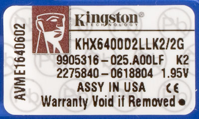
The manufacturer's web site does not publish the DDR2 Part Number expansion. Datasheet on the modules with Part Number KHX6400D2LLK2/2G runs that this product is a kit of two modules with low latencies (hence the "LL" abbreviation), 1GB each, 128M x 64 configuration, based on sixteen 64M x8 chips. The manufacturer guarantees 100% stable operation in the standard DDR2-800 mode with 4-4-4-12 timings and 2.0 V voltage. But the default mode written in the SPD chip is DDR2-800 with 5-5-5-15 timings and the voltage of 1.8 V.
Chip Part Number Expansion
Like in the previously reviewed Kingston HyperX DDR2-900, these memory modules use chips with the original designation of their real manufacturer (Elpida). So we can examine their characteristics and study the data sheet on 512-Mbit DDR2 Elpida memory chips, used in these modules.
| Field |
Value |
Expansion |
| 0 |
— |
Manufacturer (n/a, "E" = Elpida Memory) |
| 1 |
— |
Type (n/a, "D" = monolithic device) |
| 2 |
E |
Product family: "E" = DDR2 |
| 3 |
51 |
Capacity/Logical Banks: "51" = 512Ì/4
banks |
| 4 |
08 |
Organization: "08" = x8 |
| 5 |
A |
Power supply, Interface: "A" = SSTL
1.8V |
| 6 |
G |
Die revision: "G" |
| 7 |
— |
Package code (n/a, "SE" = FBGA) |
| 8 |
6E |
Speed: "6E" = DDR2-667 (5-5-5) |
| 9 |
E |
Environment code: "E" = Lead free |
As usual, designation of these Elpida chips lacks fields for the manufacturer (Elpida Memory), device type (monolithic), as well as package code (FBGA). As you can see on the table, the module chips are of the 64M x8 setup (full capacity — 512 Mbit). They are designed for the slow DDR2-667 mode (5-5-5 timings), which corresponds to the first revision of the DDR2-667 standard. Note that the same chips (but from the other manufacturer) are used in higher-speed Kingston HyperX DDR2-900 modules, which we already reviewed. To all appearances, we can speak of thorough selection of DDR2-667 chips by the manufacturer to get the highest-speed and the most reliable samples, instead of using real DDR2-800 chips.
SPD chip data
Description of the general SPD standard:
Description of the specific SPD standard for DDR2:
| Parameter |
Byte |
Value |
Expansion |
| Fundamental Memory Type |
2 |
08h |
DDR2 SDRAM |
| Number of Row Addresses on this assembly |
3 |
0Eh |
14 (RA0-RA13) |
| Number of Column Addresses on this assembly |
4 |
0Ah |
10 (CA0-CA9) |
| Number of DIMM Banks |
5 |
61h |
2 physical banks |
| Data Width of this assembly |
6 |
40h |
64 bit |
| Voltage Interface Level of this assembly |
8 |
05h |
SSTL 1.8V |
| SDRAM Cycle time (tCK) at maximum supported
CAS# latency (CL X) |
9 |
25h |
2.50 ns (400.0 MHz) |
| DIMM configuration type |
11 |
00h |
Non-ECC |
| Refresh Rate/Type |
12 |
82h |
7.8125 ms — 0.5x reduced self-refresh |
| Primary SDRAM Width (organization type) of the
memory module chips |
13 |
08h |
x8 |
| Error Checking SDRAM Width (organization type)
of the memory chips in the ECC module |
14 |
00h |
Not defined |
| Burst Lengths Supported (BL) |
16 |
0Ch |
BL = 4, 8 |
| Number of Banks on SDRAM Device |
17 |
04h |
4 |
| CAS Latency (CL) |
18 |
38h |
CL = 5, 4, 3 |
| Minimum clock cycle (tCK) at reduced
CAS# latency (CL X-1) |
23 |
3Dh |
3.75 ns (266.7 MHz) |
| Minimum clock cycle (tCK) at reduced
CAS# latency (CL X-2) |
25 |
50h |
5.00 ns (200.0 MHz) |
| Minimum Row Precharge Time (tRP) |
27 |
32h |
12.5 ns
5.0, CL = 5
3.3, CL = 4
2.5, CL = 3 |
| Minimum Row Active to Row Active delay (tRRD) |
28 |
1Eh |
7.5 ns
3.0, CL = 5
2.0, CL = 4
1.5, CL = 3 |
| Minimum RAS to CAS delay (tRCD) |
29 |
32h |
12.5 ns
5.0, CL = 5
3.3, CL = 4
2.5, CL = 3 |
| Minimum Active to Precharge Time (tRAS) |
30 |
27h |
39.0 ns
15.6, CL = 5
10.4, CL = 4
7.8, CL = 3 |
| Module Bank Density |
31 |
80h |
512 MB |
| Write recovery time (tWR) |
36 |
3Ch |
15.0 ns
6, CL = 5
4, CL = 4
3, CL = 3 |
| Internal write to read command delay (tWTR) |
37 |
1Eh |
7.5 ns
3.0, CL = 5
2.0, CL = 4
1.5, CL = 3 |
| Internal read to precharge command delay (tRTP) |
38 |
1Eh |
7.5 ns
3.0, CL = 5
2.0, CL = 4
1.5, CL = 3 |
| SDRAM Device Minimum Active to Active/Auto Refresh
Time (tRC) |
41, 40 |
33h, 30h |
51.5 ns
20.6, CL = 5
13.7, CL = 4
10.3, CL = 3 |
| SDRAM Device Minimum Auto-Refresh to Active/Auto-Refresh
Command Period (tRFC) |
42, 40 |
69h, 30h |
105.0 ns
42, CL = 5
28, CL = 4
21, CL = 3 |
| Maximum device cycle time (tCKmax) |
43 |
80h |
8.0 ns |
| SPD Revision |
62 |
12h |
Revision 1.2 |
| Checksum for Bytes 0-62 |
63 |
31h |
49 (true) |
| Manufacturer’s JEDEC ID Code |
64-71 |
7Fh, 98h |
Kingston |
| Module Part Number |
73-90 |
00h...00h |
Not defined |
| Module Manufacturing Date |
93-94 |
06h, 0Fh |
Year 2006, Week 15 |
| Module Serial Number |
95-98 |
5Ah, 15h,
8Eh, 29h |
298E155Ah |
SPD data are not standard, probably due to the low latency design. Three different CAS# latencies are supported — 5, 4, and 3. The first value (CL X = 5) corresponds to DDR2-800 (2.5ns cycle time) and 5-5-5-15.6 timings (rounded up to 5-5-5-16), which approximately matches the official values, published in the documentation (5-5-5-15, DDR2-800). Strange as it may seem, the second tCL value (CL X-1 = 4) corresponds to DDR2-533 (3.75ns cycle time), not to DDR2-667. The timing scheme for this case is not composed of integer values - it can be written as 4-3.3-3.3.-10.4, to be rounded up to 4-4-4-11. And finally the third value of CAS# latency (CL X-2 = 3) corresponds to DDR2-400, again with a fractional timings scheme (3-2.5-2.5-7.8) to be rounded up to 3-3-3-8. The module features a relatively high minimum refresh to active/refresh command period tRFC = 105.0 ns, which we come across rather often in high-speed modules. SPD revision, Manufacturer’s JEDEC ID Code, Manufacturing Date and Serial Number of the module are correct. But there is no data on the module's Part Number.
Testbed configuration
- CPU: Intel Pentium 4 Extreme Edition 3.73 GHz (Prescott N0, 2 MB L2)
- Chipset: Intel 975X
- Motherboard: ASUS P5WD2-E Premium, BIOS 0404 dated 03/22/2006
- Memory: 2x1024 MB Kingston HyperX DDR2-800 Low Latency
Test Results
Performance tests
In the first series of tests we used the timing scheme, set in BIOS Setup by default (Memory Timings: "by SPD"). The modules were tested in two modes — DDR2-667 with 200 MHz and 266 MHz FSB (memory multipliers - 1.67 and 1.25 correspondingly) and DDR2-800 with 200 MHz and 266 MHz FSB (memory multipliers - 2.0 and 1.5 correspondingly). We remind you that from our previous review on, we upgrade to RMMA 3.65 with a larger memory block to be tested (32MB) by default, which greatly reduces the effect of a relatively large 2MB L2 Cache in Pentium 4 Extreme Edition processors.
In DDR2-667 mode, the motherboard's BIOS set the timings to 5-5-5-13 by default ("at random", as the SPD chip lacks the data necessary), while the default timings in DDR2-800 mode were 5-5-5-16 (by SPD).
| Parameter / Mode |
DDR2-667 |
DDR2-800 |
| FSB Clock, MHz |
200 |
266 |
200 |
266 |
| Timings |
5-5-5-13 |
5-5-5-13 |
5-5-5-16 |
5-5-5-16 |
| Average memory read bandwidth,
MB/sec |
5387 |
6406 |
5617 |
6875 |
| Average memory write bandwidth,
MB/sec |
2056 |
2252 |
2321 |
2465 |
| Max. memory read bandwidth,
MB/sec |
6491 |
8232 |
6528 |
8541 |
| Max. memory write bandwidth,
MB/sec |
4282 |
5660 |
4279 |
5679 |
| Minimum Pseudo-Random
Access Latency, ns |
56.6 |
50.0 |
52.5 |
45.5 |
| Maximum Pseudo-Random
Access Latency, ns |
66.2 |
57.3 |
61.7 |
53.0 |
| Minimum Random Access
Latency*, ns |
118.8 |
105.3 |
106.0 |
95.4 |
| Maximum Random Access
Latency*, ns |
143.8 |
123.9 |
130.2 |
115.5 |
Minimum Pseudo-Random
Access Latency, ns
(without hardware prefetch) |
87.0 |
78.2 |
80.3 |
70.4 |
Maximum Pseudo-Random
Access Latency, ns
(without hardware prefetch) |
113.7 |
96.5 |
107.3 |
90.1 |
Minimum Random Access
Latency*, ns
(without hardware prefetch) |
119.6 |
105.5 |
106.2 |
95.9 |
Maximum Random Access
Latency*, ns
(without hardware prefetch) |
145.5 |
125.0 |
133.7 |
116.6 |
*32 MB block size
Performance results of these modules are quite high — maximum real memory bandwidth is approximately 6.4-6.5 GB/s with 200-MHz FSB and 8.2-8.6 GB/s with 266-MHz FSB, that is it practically reaches the theoretical maximum in FSB bandwidth (it's even slightly higher due to the effect of L2 Cache in a processor). As usual, memory access latencies are decreased in faster modes (when you go from DDR2-667 to DDR2-800) as well as with higher-clocked FSB (when you go from 200-MHz to 266-MHz FSB). Minimum memory latency in DDR2-800 with 266 MHz FSB is from 45.5 ns (pseudo-random walks, enabled hardware prefetch) to 116.6 ns (random walks, disabled hardware prefetch), which is a tad worse than the results of higher-ranked Kingston HyperX DDR2-900 modules.
Stability tests
Timing values, except for tCL, were adjusted "on the fly" due to the built-in RMMA feature that allows to change dynamically memory settings supported by the chipset. Memory operating stability was evaluated with an auxiliary utility RightMark Memory Stability Test, included into RMMA.
| Parameter / Mode |
DDR2-667 |
DDR2-800 |
| FSB Clock, MHz |
200 |
266 |
200 |
266 |
| Timings |
3-4-4
(2.0 V) |
3-4-4
(2.0 V) |
4-5-4-12
(2.0 V) |
4-5-4-12
(2.0 V) |
| Average memory read bandwidth,
MB/sec |
5537 |
6798 |
5652 |
6990 |
| Average memory write bandwidth,
MB/sec |
2260 |
2465 |
2358 |
2613 |
| Max. memory read bandwidth,
MB/sec |
6501 |
8331 |
6515 |
8632 |
| Max. memory write bandwidth,
MB/sec |
4282 |
5664 |
4281 |
5675 |
| Minimum Pseudo-Random
Access Latency, ns |
53.1 |
46.1 |
49.3 |
44.4 |
| Maximum Pseudo-Random
Access Latency, ns |
62.5 |
53.3 |
59.0 |
51.8 |
| Minimum Random Access
Latency*, ns |
109.6 |
95.4 |
105.5 |
92.7 |
| Maximum Random Access
Latency*, ns |
133.9 |
114.9 |
129.7 |
112.7 |
Minimum Pseudo-Random
Access Latency, ns
(without hardware prefetch) |
81.9 |
70.9 |
75.2 |
68.5 |
Maximum Pseudo-Random
Access Latency, ns
(without hardware prefetch) |
107.9 |
93.2 |
102.0 |
88.4 |
Minimum Random Access
Latency*, ns
(without hardware prefetch) |
110.4 |
95.9 |
105.8 |
93.1 |
Maximum Random Access
Latency*, ns
(without hardware prefetch) |
136.6 |
116.7 |
132.6 |
113.6 |
*32 MB block size
Strange as it may seem, the minimum timings, we managed to obtain in DDR2-667 mode with the recommended increased voltage of 2.0 V, look quite unassuming - 3-4-4 (tRAS is ignored in this case.) By the way, we managed to set much better timings (3-3-2) for Kingston HyperX DDR2-900 under these conditions. The situation in DDR2-800 is still worse — minimum timings possible (stable) were only 4-5-4-12, even higher than the official 4-4-4-12 scheme. Interestingly, tRAS makes a determining contribution to memory stability in this case — its reduction results in an immediate system freeze.
As usual, "extreme" timings only insignificantly increase memory bandwidth, the effect is noticeable only in random access latencies. Maximum effect of reduced latencies is reached in DDR2-667 - about 9 ns, that is approximately 8%.
Bottom line
High-capacity Kingston HyperX DDR2-800 modules (PC2-6400) with "low latencies" can operate in DDR2-667 and DDR2-800 modes in nominal conditions (that is with standard timings, like 5-5-5-15 for DDR2-800) and are characterized by high performance in these modes. At the same time, the overclocking potential of these modules as far as timings are concerned leaves much to be desired. So we can hardly refer to them as "Low Latency" modules. The minimum timings possible in DDR2-667 mode that do not damage memory operation stability are just 3-4-4 (with the recommended voltage of 2.0V). What concerns DDR2-800 — 4-5-4-12, which is even worse than 4-4-4-12, official values published in the documentation. At least on the ASUS P5WD2-E motherboard (we use it in our tests), which proved itself a trustworthy model for testing high-speed DDR2 memory modules.
Write a comment below. No registration needed!
|
|
 |
|
|
|