Memory Module Analysis. Part 19: Kingston HyperX DDR2-900 (PC2-7200)
|
We proceed with the low-level analysis of the most important characteristics of high-performance DDR2 memory modules using our RightMark Memory Analyzer. Our today's analysis is devoted to the dual channel kit of high-end HyperX-series Kingston modules, intended for the unofficial DDR2-900 mode (PC2-7200). This kit comes in 512 MB, 1 GB, and 2 GB modifications, which differ from each other in memory size only. We already reviewed Kingston modules of this series (KHX6000D2K2/1G DDR2-750 modules). Nevertheless, we didn't test modules in high-speed DDR2-667, DDR2-800, and higher modes at that time yet — mostly because there was no need in such modes (in fact, these modes are not needed even now). In this article we'll analyze performance of these modules (1GB modification) in standard DDR2-667 and DDR2-800 modes as well as in unofficial DDR2-900 mode, which is still mentioned by the manufacturer.
Manufacturer Information
Module manufacturer: Kingston Technology
Manufacturer of module chips: Infineon
Web site of the module manufacturer:
http://www.kingston.com/hyperx/products/khx_ddr2.asp
Web site of the chip manufacturer: here
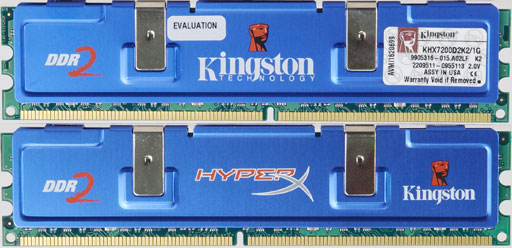
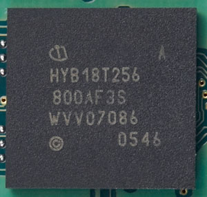
Module Exterior
Photo of the memory module
Photo of the memory chip
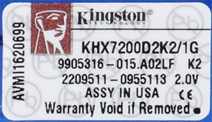
Module Part Number
Module Part Number Expansion
The manufacturer's web site does not publish the DDR2 Part Number expansion. Datasheet on the modules with Part Number KHX7200D2K2/1G specifies that the product is a kit of two 512MB modules, 64M x 64, based on 64M x 8 chips. The modules belong to the unofficial DDR2-900 group and can operate in this mode with CAS# latency = 5. The manufacturer guarantees 100% stable operation in DDR2-900 mode with 5-5-5-15 timings and 2.0 V voltage. But the default mode written in the SPD chip is standard DDR2-667 with 5-5-5-15 timing and the voltage of 1.8 V.
Chip Part Number Expansion
Unlike previous high-speed modules of the HyperX series (KHX6000D2K2/1G), these modules use chips with the original designation of their real manufacturer (Infineon), which allows us to examine their characteristics using the latest nomenclature version of DRAM components available on the manufacturer's web site.
| Field |
Value |
Expansion |
| 0 |
HYB |
Prefix: "HYB" = memory components |
| 1 |
18 |
Voltage: "18" = 1.8 V |
| 2 |
T |
Memory type: "T" = DDR2 SDRAM |
| 3 |
256 |
Chip capacity: "256" = 256 Mbit |
| 4 |
80 |
Organization: "80" = x8 |
| 5 |
O |
Product modification: "O" = standard product |
| 6 |
A |
Die revision: "A" |
| 7 |
F |
Package: "F" = FBGA |
| 8 |
3S |
Performance characteristics: "3S" = DDR2-667, 5-5-5 timings |
These characteristics show that the modules are based on 256Mbit chips with 32M x8 organization. What's most interesting, these chips are intended for DDR2-667 mode, moreover, for its modification with slower timings 5-5-5 (faster DDR2-667 with 4-4-4 timings is denoted by "3"), which contrasts the official characteristics (DDR2-900, 5-5-5-15). But it may be the reason why the default mode written in SPD is the standard DDR2-667 mode, 5-5-5-15 timings, 1.8V.
SPD chip data
Description of the general SPD standard:
Description of the specific SPD standard for DDR2:
| Parameter |
Byte |
Value |
Expansion |
| Fundamental Memory Type |
2 |
08h |
DDR2 SDRAM |
| Number of Row Addresses on this assembly |
3 |
0Dh |
13 (RA0-RA12) |
| Number of Column Addresses on this assembly |
4 |
0Ah |
10 (CA0-CA9) |
| Number of DIMM Banks |
5 |
61h |
2 physical banks |
| Data Width of this assembly |
6 |
40h |
64 bit |
| Voltage Interface Level of this assembly |
8 |
05h |
SSTL 1.8V |
| SDRAM Cycle time (tCK) at maximum supported CAS# latency (CL X) |
9 |
30h |
3.00 ns (333.3 MHz) |
| DIMM configuration type |
11 |
00h |
Non-ECC |
| Refresh Rate/Type |
12 |
82h |
7.8125 ms — 0.5x reduced self-refresh |
| Primary SDRAM Width (organization type) of the memory module chips |
13 |
08h |
x8 |
| Error Checking SDRAM Width (organization type) of the memory chips in the ECC module |
14 |
00h |
Not defined |
| Burst Lengths Supported (BL) |
16 |
0Ch |
BL = 4, 8 |
| Number of Banks on SDRAM Device |
17 |
04h |
4 |
| CAS Latency (CL) |
18 |
38h |
CL = 5, 4, 3 |
| Minimum clock cycle (tCK) at reduced CAS# latency (CL X-1) |
23 |
3Dh |
3.75 ns (266.7 MHz) |
| Minimum clock cycle (tCK) at reduced CAS# latency (CL X-2) |
25 |
50h |
5.00 ns (200.0 MHz) |
| Minimum Row Precharge Time (tRP) |
27 |
3Ch |
15.0 ns
5, CL = 5
4, CL = 4
3, CL = 3 |
| Minimum Row Active to Row Active delay (tRRD) |
28 |
1Eh |
7.5 ns
2.5, CL = 5
2.0, CL = 4
1.5, CL = 3 |
| Minimum RAS to CAS delay (tRCD) |
29 |
3Ch |
15.0 ns
5, CL = 5
4, CL = 4
3, CL = 3 |
| Minimum Active to Precharge Time (tRAS) |
30 |
2Dh |
45.0 ns
15, CL = 5
12, CL = 4
9, CL = 3 |
| Module Bank Density |
31 |
40h |
256 MB |
| Write recovery time (tWR) |
36 |
3Ch |
15.0 ns
5, CL = 5
4, CL = 4
3, CL = 3 |
| Internal write to read command delay (tWTR) |
37 |
1Eh |
7.5 ns
2.5, CL = 5
2.0, CL = 4
1.5, CL = 3 |
| Internal read to precharge command delay (tRTP) |
38 |
1Eh |
7.5 ns
2.5, CL = 5
2.0, CL = 4
1.5, CL = 3 |
| SDRAM Device Minimum Active to Active/Auto Refresh Time (tRC) |
41, 40 |
3Ch, 00h |
60.0 ns
20, CL = 5
16, CL = 4
12, CL = 3 |
| SDRAM Device Minimum Auto-Refresh to Active/Auto-Refresh Command Period (tRFC) |
42, 40 |
69h, 00h |
105.0 ns
35, CL = 5
28, CL = 4
21, CL = 3 |
| Maximum device cycle time (tCKmax) |
43 |
80h |
8.0 ns |
| SPD Revision |
62 |
12h |
Revision 1.2 |
| Checksum for Bytes 0-62 |
63 |
31h |
49 (true) |
| Manufacturer’s JEDEC ID Code |
64-71 |
7Fh, 98h |
Kingston |
| Module Part Number |
73-90 |
00h...00h |
Not defined |
| Module Manufacturing Date |
93-94 |
06h, 07h |
Year 2006, Week 7 |
| Module Serial Number |
95-98 |
68h, 1Dh,
66h, 44h |
44661D68h |
SPD contents look quite standard. Three different CAS# latencies are supported — 5, 4, and 3. The first value (CL X = 5) corresponds to DDR2-667 (3.0 ns cycle time) with 5-5-5-15 timings, which matches the official values, specified in the documentation. The second value tCL (CL X-1 = 4), as usual, corresponds to DDR2-533 with 4-4-4-12 timings. And finally, the third value (CL X-2 = 3) — DDR2-400 with 3-3-3-9 timings. The module features a relatively high minimum refresh to active/refresh command period tRFC = 105.0 ns, which we come across rather often in high-speed modules. SPD revision, Manufacturer’s JEDEC ID Code, Manufacturing Date and Serial Number of the module are correct. But there is no data on the module's Part Number.
Testbed configuration
- CPU: Intel Pentium 4 Extreme Edition 3.73 GHz (Prescott N0, 2 MB L2)
- Chipset: Intel 975X
- Motherboard: ASUS P5WD2-E Premium, BIOS 0206 dated 12/21/2005
- Memory: 2x512 MB Kingston HyperX DDR2-900
Test Results
Performance tests
In the first series of tests we used the timing scheme, set in BIOS Setup by default (Memory Timings: "by SPD"). The modules were tested in three modes — DDR2-667 with 200 MHz and 266 MHz FSB (memory multipliers - 1.67 and 1.25), DDR2-800 with 200 MHz and 266 MHz FSB (memory multipliers - 2.0 and 1.5), as well as "DDR2-900" with FSB overclocked to 225 MHz and 270 MHz (memory multipliers - 2.0 and 1.67).
As you can see on the table below, BIOS sets correct timings by default for DDR2-667 mode — 5-5-5-15, while in case of DDR2-800 and DDR2-900 modes the motherboard uses more conservative 5-6-6-18 timings by default, set by BIOS "at random", as SPD does not contain data for faster official DDR2-800 mode.
| Parameter / Mode |
DDR2-667 |
DDR2-800 |
DDR2-900 |
| FSB Clock, MHz |
200
|
266
|
200
|
266
|
225
|
270
|
| Timings |
5-5-5-15 |
5-5-5-15 |
5-6-6-18 |
5-6-6-18 |
5-6-6-18 |
5-6-6-18 |
| Average memory read bandwidth,
MB/sec |
5406
|
6425
|
5605
|
6859
|
6253
|
7110
|
| Average memory write bandwidth,
MB/sec |
2144
|
2377
|
2216
|
2513
|
2597
|
2743
|
| Max. memory read bandwidth,
MB/sec |
6813
|
8614
|
6853
|
8923
|
7640
|
9096
|
| Max. memory write bandwidth,
MB/sec |
4282
|
5685
|
4282
|
5697
|
4808
|
5770
|
| Minimum Pseudo-Random Access
Latency, ns |
56.3
|
49.9
|
52.5
|
45.5
|
46.9
|
43.1
|
| Maximum Pseudo-Random Access
Latency, ns |
65.8
|
57.0
|
61.8
|
53.0
|
55.4
|
50.3
|
| Minimum Random Access Latency*,
ns |
114.5
|
101.8
|
107.5
|
94.8
|
96.0
|
89.1
|
| Maximum Random Access Latency*,
ns |
138.7
|
120.2
|
131.6
|
113.6
|
117.5
|
107.9
|
Minimum Pseudo-Random Access
Latency, ns
(without hardware prefetch) |
86.5
|
77.4
|
80.6
|
70.5
|
72.3
|
66.6
|
Maximum Pseudo-Random Access
Latency, ns
(without hardware prefetch) |
112.6
|
97.0
|
106.6
|
90.2
|
95.8
|
85.8
|
Minimum Random Access Latency*,
ns
(without hardware prefetch) |
115.4
|
102.8
|
108.9
|
96.0
|
97.3
|
90.2
|
Maximum Random Access Latency*,
ns
(without hardware prefetch) |
141.1
|
122.4
|
136.4
|
115.9
|
120.4
|
109.5
|
*16 MB block size
Performance results of the modules look good — maximum memory bandwidth values in official modes amount to approximately 6.8 GB/s and 8.9 GB/s at the FSB clock set to 200 MHz and 266 MHz. This is typical of high-speed modules operating with a processor with 2MB L2 Cache. These modules are also no worse than their high-speed counterparts from the other manufacturers in latencies. As usual, latencies decrease in faster modes (when you go from DDR2-667 to DDR2-800 and DDR2-900) as well as with higher clocked FSB (when you go from 200 MHz to 266/270 MHz FSB). Thus, minimal memory latency is demonstrated in DDR2-900 mode with the 270 MHz FSB, falling between 43.1 ns (pseudo-random walks, hardware prefetch enabled) and 109.5 ns (random walks, hardware prefetch disabled).
Stability tests
Timing values, except for tCL, were adjusted "on the fly" due to the built-in RMMA feature that allows to change dynamically memory settings supported by the chipset. Memory operating stability was evaluated with an auxiliary utility RightMark Memory Stability Test, included into RMMA.
| Parameter / Mode |
DDR2-667 |
DDR2-800 |
DDR2-900 |
| FSB Clock, MHz |
200
|
266
|
200
|
266
|
225
|
270
|
| Timings |
3-3-2
(2.0 V)
|
3-3-2
(2.0 V)
|
4-4-2
(2.0 V)
|
4-4-2
(2.0 V)
|
4-4-3
(2.0 V)
|
4-4-3
(2.0 V)
|
| Average memory read bandwidth,
MB/sec |
5575
|
6839
|
5704
|
7045
|
6325
|
7324
|
| Average memory write bandwidth,
MB/sec |
2454
|
2829
|
2465
|
3111
|
2760
|
3191
|
| Max. memory read bandwidth,
MB/sec |
6843
|
8806
|
6868
|
9081
|
7705
|
9233
|
| Max. memory write bandwidth,
MB/sec |
4282
|
5692
|
4282
|
5698
|
4808
|
5770
|
| Minimum Pseudo-Random Access
Latency, ns |
52.7
|
45.9
|
49.1
|
44.4
|
46.5
|
41.7
|
| Maximum Pseudo-Random Access
Latency, ns |
62.0
|
53.2
|
58.6
|
51.7
|
54.8
|
48.8
|
| Minimum Random Access Latency*,
ns |
100.8
|
89.8
|
96.8
|
87.3
|
89.9
|
82.0
|
| Maximum Random Access Latency*,
ns |
124.2
|
108.2
|
120.7
|
105.9
|
110.9
|
100.0
|
Minimum Pseudo-Random Access
Latency, ns
(without hardware prefetch) |
81.2
|
71.0
|
74.7
|
68.5
|
71.1
|
64.5
|
Maximum Pseudo-Random Access
Latency, ns
(without hardware prefetch) |
106.9
|
91.7
|
102.4
|
88.6
|
95.1
|
84.4
|
Minimum Random Access Latency*,
ns
(without hardware prefetch) |
101.6
|
90.8
|
97.6
|
88.2
|
91.0
|
82.7
|
Maximum Random Access Latency*,
ns
(without hardware prefetch) |
128.5
|
110.8
|
125.0
|
108.8
|
114.6
|
103.1
|
*16 MB block size
Minimum timings, we managed to obtain in DDR2-667 mode with the recommended voltage of 2.0 V, look impressive — 3-3-2 (as usual, the last parameter tRAS does not participate in the overclocking scheme, as it's ignored). A smaller, absolute record — 3-2-2 (timings cannot be reduced any further) with the recommended voltage of 2.1 V was broken only by Corsair XMS2-5400UL modules. The same can be said about DDR2-800 mode — in this case, minimal timings in the modules under review are 4-4-2, again slightly outperformed by Corsair XMS2-5400UL modules with their record of 4-3-2. And finally, minimal timings in the overclocked unofficial DDR2-900 mode are no less attractive — to obtain stable operation of the modules, we only had to increment tRP by one compared to the previous scheme.
As usual, "extreme" timings only insignificantly increase memory bandwidth, as it's still limited by FSB bandwidth. Maximum effect of this "timings overclocking" is noticeable only in terms of latencies, only in case of random memory access at that — latencies are reduced by 10%.
Bottom line
Kingston HyperX DDR2-900 (PC2-7200) modules under review (1GB dual channel kit) proved themselves as high-end high-speed modules that can operate in official DDR2-667 and DDR2-800 modes as well as in the unofficial DDR2-900 mode, which is still mentioned by the manufacturer (with relatively low voltage of 2.0 V, compared to the nominal value). The modules offer high performance and noticeable "overclocking of timings" in the modes we tested — in the official DDR2-667 and DDR2-800 modes they can operate with 3-3-2 and 4-4-2 timings (which is very close to the records, broken by Corsair XMS2-5400UL modules), while operation in DDR2-900 mode requires increasing timings to "extreme" 4-4-3.
Write a comment below. No registration needed!
|
|
 |
|
|
|