 |
||
|
||
| ||
|
||
|
||
| ||
We continue our analysis of the primary features of high-speed DDR2 memory modules today by taking a look at a new high-end product from the Corsair DOMINATOR series, the 2GB DDR2-1250 dual-channel kit. We will be analyzing performance of the modules using our RightMark Memory Analyzer tool, which is freely available on the web. These memory modules are the pinnacle of DDR2 technology, and also might have reached the final capacity of the DDR2 standard. This means that these modules very well might be the last DDR2-based modules in the Corsair Dominator series of products. Manufacturer informationModule manufacturer: Corsair Memory Chip manufacturer: unknown Manufacturer's website: http://www.corsairmemory.com/corsair/dominator.html Module exterior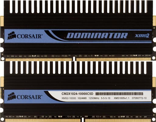 The modules that are being reviewed look identical to the Corsair TWIN2X2048-9136C5D and TWIN2X2048-8888C4D entry level DOMINATOR products. One feature that distinguishes products in the DOMINATOR series is the new Dual-path Heat Xchange cooling technology. In essence, Corsair claims this cooling solution removes more heat in two ways; by using extruded aluminum heatsinks with “optimized” fins to increase airflow and dissipate more heat and by using a dedicated heatsink for the PCB itself. 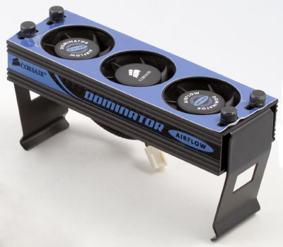 These modules can be additionally cooled by the supplied DOMINATOR Airflow Fans system which creates direct airflow to modules for improved heat removal. Module part number Unfortunately, at the Corsair company website we were unable to find a part number guide for the DOMINATOR DDR2 series. The TWIN2X2048-10000N5DF product sheet states that the kit consists of 2 x 1GB CM2X1024-10000N5D modules. The modules support Enhaned Performance Profiles (Serial Presence Detect extension), an open standard jointly created by Corsair and NVIDIA. EPP allows memory settings to be automatically optimized on motherboards that support EPP. It has been developed primarily to make overclocking easier. Corsair guarantees that the modules will work at DDR2-1250 speeds with EPP timings of 5-5-5-18-2T and a rather «extreme» voltage of 2.4 V on motherboards based on the NVIDIA nForce 680i SLI EVGA chipset. At that voltage setting, by default the SPD sets memory speed to DDR2-800 mode at 5-5-5-18 timings. SPD DataGeneral SPD standard specification: DDR2 SPD standard specification:
Taking a look at the SPD chip on the modules, the part number of the SPD ROM of the modules under review today matches up to the number of the SPD chip on the previously reviewed CM2X1024-9136C5D and CM2X1024-8888C4D modules. The maximum performance that today's modules are designed for is a 2.5 ns cycle time (400 MHz frequency, DDR2-800). The first of the supported values is tCL = 5, while the complete timing scheme is 5-5-5-18, which agrees with what the manufacturer states in its brief documentation for the memory kit. Lower CAS# signal latency values (CL X-1 = 4) can be achieved using a non-standard clock signal period of 3.7 ns (typical for Corsair memory modules), which corresponds to a frequency of approximately 270 MHz. Most likely , this setting is meant for DDR2-533 mode with a 3.75 ns cycle time. An improper clock signal period value leads to non-integer values in the timing scheme, which can be written (rounded to one decimal place) as 4-3.4-3.4-12.2 and rounded up to integer values, as 4-4-4-13. As a matter of fact, DDR2-533 is obsolete in today's day and age, especially for such high-speed modules, so these values hardly bear any true significance. In our opinion, this setting should have been excluded from the SPD memory quite some time ago. Although the manufacturer identification code along with the module part number is stated correctly, as is true with other Corsair modules, the SPD chip does not give details regarding the manufacturing date and serial number. In this case, they are filled with a value of FFh. Now let us look at the most critical information in the «non-standard» part of the SPD, bytes 99-127 of the SPD memory which contains the EPP profiles. EPP standard specification:
The modules being examined support Enhanced Performance Profiles and contain information for two «extended» profiles. Of the two enhanced profiles, only the second one (Profile #1) is operative and is, naturally, marked as recommended by default. This profile has a cycle time of 1.60 ns, meaning it has a frequency of 625 MHz; a «DDR2-1250» rating. The timings of this profile can not be completely represented using integers and is written as 5-5-5-17.5, which, evidently, should be interpreted by motherboards supporting EPP as 5-5-5-18. Delays in address-command interface for this profile amount to 2T while the modules' power supply voltage is at 2.4 V. The minimum row cycle time (tRC), is a mere 15 cycles of external data bus, a rather small value which comes as a bit of a surprise, primarily because it turns out to be less than the tRASparameter, which is 17.5 (18) cycles of external data bus. It is possible that this in fact is a mistake that was made on the manufacturer's part when coding the EPP profile data. Testbed configurationTestbed #1
Testbed #2
Test resultsWe examined the TWIN2X2048-10000C5DF modules using two platforms equipped with the following processors: AMD Athlon 64 X2 5200+ (ASUS CROSSHAIR motherboard, testbed #1) and Intel Core 2 Duo E6600 (NVIDIA reference motherboard with nForce 680i chipset, testbed #2). Both motherboards support EPP standard providing compatibility with the modules being reviewed. The modules were tested in the following modes:
In all cases the memory modules were provided with additional cooling by the supplied DOMINATOR Airflow cooling system.
* - For a 32 MB block. In standard DDR2-800 mode the platform based on the AMD Athlon 64 X2 5200+ CPU (testbed #1) uses the standard timing scheme of 5-5-5-18-2T which is stored in the standard part of the SPD memory. The timing scheme, which we managed to achieve in this case while raising power supply voltage for the modules up to the manufacturer recommended level of 2.4 V, was the smallest possible values we could achieve (for the given platform): 3-3-3-2T. However, we cannot say that the timings affected the speed characteristics of the memory subsystem in a fundamental way. The reason is because the relatively low CPU clock rate which we had to use at this stage of testing (200x12 = 2400 MHz) slowed down our system. The most surprising result we saw in our tests came when trying to use maximum performance mode (with settings from the EPP profile). Under this mode, the CPU would be overclocked 15%, meaning it would be hitting 3 GHz (300 MHz FSB x 10) — Using this performance profile we were not even able to boot into the system's operating system, let alone running stability tests and performance measurements. Moreover, neither the CPU nor the motherboard turned out to be «at fault», but rather the memory modules themselves were the culprit. We were able to successfully boot the system with the CPU overclocked to 3000 MHz (CPU core voltage in all cases was raised to 1.45 V) while we forced the memory to run at lower speeds. The maximum possible memory speed the modules reached using EPP profile data was a mere 500 MHz (i.e. «DDR2-1000»). Further increasing the speed of the modules to 520 MHz led to errors during our memory stability tests. However, the slight overclock did not create a complete system failure. The overclocking of the modules weren't a complete failue, as we were able to lower the module timings from 5-5-5-18-2T to rather small values of 4-4-3-2T. This is not a feat that all memory modules can achieve at DDR2-1000 speeds. Let's move on to considering the results obtained with our second Intel Core 2 Duo E6600 CPU test platform based on the NVIDIA nForce 680i SLI chipset (testbed #2). Fortunately, all tests on this platform were successful. In standard DDR2-800 mode the Intel Core 2 Duo system, using standard settings from the SPD, ran at timings of 5-5-5-18-2T with nominal power supply voltage (1.85 V). By raising the voltage to 2.4 V, we succeeded in lowering the timings to the same values obtained on the first test platform — 3-3-3-2T. Furthermore, due to the NVIDIA nForce 680i SLI chipset allowing the use of timings up to 1-1-1 (!) we were able to get the BIOS to load at an even more impressive timing scheme; 3-3-2-2T. Loading the operating system to run tests proved impossible at those timings, though, as the system crashed. We were still glad that we got past the BIOS stage, however. Nevertheless, similar to the case of the AMD platform, the considerable decrease in memory timing s led to very small changes in the memory subsystem's actual speed, which is bound to a rather low CPU clock rate (2.4 GHz) along with chipset memory controller limitations. The DDR2-1250 mode, which is stored in the in EPP profile, was practically achieved (memory bus frequency of 622 MHz, i.e. 1244 «DDR2 MHz») without overclocking the CPU at all. This is because of the nForce 680i SLI chipset's ability to tune to an asynchronous operating mode in a fairly flexible way — the ratio of the memory bus frequency to the system bus frequency on this chipset can take on various values (in this case — 35/15 = 2.333) with a small enough increment (1/15), which means an increment of memory bus frequency of about 18 MHz. The timing scheme in this case is the same as the EPP data — 5-5-5-18-2T, and the power supply voltage for the modules also conforms with the recommended 2.4 V. Despite the significant increase in memory frequency (from 400 to 622 MHz), differences in memory bandwidth values between these two operating modes turn out to be virtually unnoticeable (somewhat more evident are the differences between random ac cess latencies). This reconfirms that using such high-speed memory on the Intel platform (with not the most high-speed 2.4-GHz Intel Core 2 Duo E6600 CPU) ends up being completely unjustified. Finally, we also evaluated the possibility of testing the modules at maximum frequency. In the process, we naturally overclocked the CPU also. The maximum memory frequency without loss of stability that we achieved came out to be 645 MHz («DDR2-1290») — barely below the «DDR2-1300» mark. The timing scheme in this case was automatically increased by the motherboard BIOS to 5-6-6-19-2T. Attempting to lower these timings led to system errors and instability. ConclusionThe examined high-end modules from the Corsair DOMINATOR series, the TWIN2X2048-10000C5DF memory modules, left a good impression on us with its maximum frequency of DDR2-1250. The only problem we saw in the tests was the somewhat limited compatibility of the modules with our AMD-based test platform, which consisted of an Athlon 64 X2 5200+ CPU along with an ASUS Crosshair motherboard. With this platform, the maximum bus frequency at which the modules were considered farily stable, was merely 500 MHz, or DDR2-1000. We are hoping that the uncovered problem is only an issue with our platform itself, namely the certain combination of CPU, motherboard and BIOS we were using, and not the AMD AM2 platform as a whole. In regards to the Intel/NVIDIA platform, which was based on an Intel Core 2 Duo CPU and the nForce 680i chipset, the modules under review demonstrated exceptional compatibility and were fully operable under regular conditiona at DDR2-800 paired with record-low timings of 3-3-3-2T and a voltage level of 2.4 Volts. The maximum we reached with this platform was another record for us, and we ended up at a memory bus frequency of 645 MHz, which equates to DDR2-1290, at 2.4 Volts. The timings were automatically adjusted by the motherboard to 5-6-6-29-2T. Dmitriy Besedin (dmitri_b@ixbt.com)
July 25, 2007 Write a comment below. No registration needed!
|
Platform · Video · Multimedia · Mobile · Other || About us & Privacy policy · Twitter · Facebook Copyright © Byrds Research & Publishing, Ltd., 1997–2011. All rights reserved. | |||||||||||||||||||||||||||||||||||||||||||||||||||||||||||||||||||||||||||||||||||||||||||||||||||||||||||||||||||||||||||||||||||||||||||||||||||||||||||||||||||||||||||||||||||||||||||||||||||||||||||||||||||||||||||||||||||||||||||||||||||||||||||||||||||||||||||||||||||||||||||||||||||||||||||||||||||||||||||||||||


