 |
||
|
||
| ||
|
||
|
||
| ||
We proceed with the analysis of the most important characteristics of high-performance DDR2 memory modules using our RightMark Memory Analyzer. Today we are going to examine another top product from Corsair — memory modules of the new DOMINATOR series, unofficial "DDR2-1142" and "DDR2-1111". They are designed to reveal potential of the new NVIDIA nForce 680i SLI platform. Manufacturer InformationModule manufacturer: Corsair Memory Exterior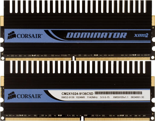 Design of new DOMINATOR modules (the photo shows XMS2-9136C5D modules) suffered significant changes. First of all, these changes have to do with a principally new cooling technology, called Dual-path Heat Xchange (DHX(tm)). This technology consists in channelling the heat away in two ways — through BGA chip contacts to a PCB of the module as well as from the package of BGA chips to highly efficient heatsinks made of extruded aluminum. 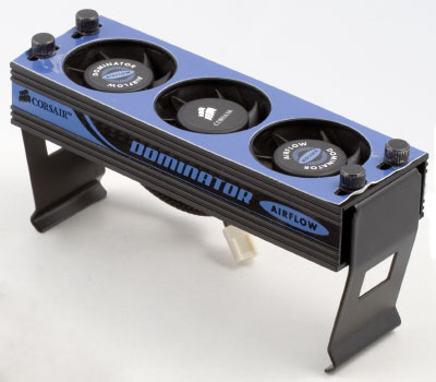 DOMINATOR modules can also be cooled by the new system - DOMINATOR Airflow Fans. It creates a direct airflow to memory modules for improved heat dissipation and channelling the heat away from the memory modules. In our case, this cooling system came shipped with slower, but more extreme in terms of timings (as well as voltage) XMS2-8888C4D memory modules. Module Part NumberXMS2-9136C5D The manufacturer's web site does not publish the DDR2 Part Number expansion of XMS2 DOMINATOR series memory modules. The datasheet on TWIN2X2048-9136C5D modules specifies that it's a bundle of two CM2X1024-9136C5D modules, 1 GB each. These modules support the open standard EPP (SPD extension), developed by Corsair and NVIDIA. It allows to configure memory modules for maximum performance automatically on motherboards that support this standard. The manufacturer guarantees that the modules will work in "DDR2-1142" mode with 5-5-5-15-2T timings from a EPP profile and at 2.1 V (such a low voltage for such a fast mode is reached owing to the DHX technology). At the same time, a default mode in the standard SPD section is the maximal standard DDR2-800 mode with 5-5-5-18 timings. XMS2-8888C4D As specified in their datasheet, TWIN2X2048-8888C4D modules have similar characteristics — it's a 2 GB bundle of two 1 GB modules CM2X1024-8888C4D, supporting EPP. These modules are guaranteed to work in "DDR2-1111" mode with EPP 4-4-4-12-2T timings. Such extreme (for such a fast mode) timings do not come for free. They require raising memory voltage to 2.4 V, also specified in EPP profile. We can say that our DDR2 memory modules are getting close to old DDR modules, which nominal voltage is 2.5 V. SPD chip dataDescription of the general SPD standard:
Description of the specific SPD standard for DDR2:
XMS2-9136C5D/XMS2-8888C4D
The standard SPD sections of XMS2-9136C5D and XMS2-8888C4D modules match to within Part Number — CM2X1024-9136C5D and CM2X1024-8888C4D correspondingly. The fastest mode these modules are capable of is characterized by the cycle time of 2.5 ns (400 MHz, DDR2-800). This mode corresponds to the first of supported tCL values (tCL = 5). The full timings scheme is written as 5-5-5-18, which matches official characteristics published in the datasheets. Reduced CAS# latency (CL X-1 = 4) corresponds to the non-standard cycle time of 3.7 ns, approximately 270 MHz — it probably means DDR2-533 and the cycle time of 3.75 ns. Incorrect cycle time results in fractional timing values, which can be written as 4-3.4-3.4-12.2 (rounded to one figure after the dot) and rounded up to 4-4-4-13. DDR2-533 mode is not topical today, especially for such fast modules. So these values hardly make sense — in our opinion, it's high time to remove them from SPD. Manufacturer’s JEDEC ID Code and Part Number of the module are correct. Nevertheless, as in the other Corsair modules, the SPD chip of these modules lacks data on the manufacturing date and serial number (they are filled with FFh in these modules). Let's review the most important data from the "non-standard" SPD section that corresponds to EPP profiles, represented by Bytes 99-127 of the SPD content. EPP Standard Description:
XMS2-9136C5D
The XMS2-9136C5D modules support EPP and contain information about two "extended" profiles. Only the second profile (Profile 1) is topical, naturally marked as optimal (recommended to use by default). This profile corresponds to DDR2 mode with the 1.75 ns cycle time, that is 571 MHz, which corresponds to DDR2-1142. Timings of this profile cannot be written in integer numbers - 5-5-5-14.9. Motherboards with EPP support should detect this scheme as 5-5-5-15. Address command rate of this profile is 2T, module voltage — 2.1 V. XMS2-8888C4D
The XMS2-8886C4D modules have a similar EPP configuration— only the second of two "extended" profiles is active and "optimal". It corresponds to DDR2 mode with the cycle time of 1.8 ns, that is 555.5 MHz - "DDR2-1111". These timings again cannot be written in integer values - 4-4.03-4.03-11.67. Motherboards with EPP support should detect this scheme as 4-4-4-12. But they may round it up to 4-5-5-12. Address command rate - 2T, module voltage - 2.4 V. Testbed configurationsTestbed 1
Testbed 2
Test resultsThe XMS2-9136C5D modules were tested on two platforms, equipped with AMD Athlon 64 FX-62 (ASUS CROSSHAIR motherboard, Testbed 1) and Intel Core 2 Duo E6600 (a reference motherboard from NVIDIA based on the nForce 680i chipset, Testbed 2) correspondingly. Both motherboards support EPP to be compatible with the modules under review. As our tests were limited in time, the XMS2-8888C4D modules were tested only on the second platform. The modules were tested in the following modes in all cases: 1. Nominal: the standard CPU clock rate, 400 MHz memory (DDR2-800), EPP data are either not used (Testbed 1), or used for finetuning temporal and voltage characteristics, while the memory bus clock was specified manually (Testbed 2). 2. Optimal, corresponds to an EPP profile, but it does not allow CPU overclocking (only for AMD, Testbed 1). 3. Optimal, allows CPU overclocking, allows to reach maximum recommended memory frequency. 4. Maximum memory overclocking, allows CPU overclocking. XMS2-9136C5D
The platform based on AMD Athlon 64 FX-62 (Testbed 1) in DDR2-800 mode uses standard timings (5-5-5-18-2T), written in the standard SPD section. If we raise memory voltage to a reasonable level (2.3 V), minimal timings obtainable in this case are 3-4-3-2T. Note that the system works even with tougher timings (3-3-3-2T). But in this case there soon appear memory errors, which can be detected in RightMark Memory Stability Test. "Extreme" timings noticeably increase the maximum real memory bandwidth (from 8.60 GB/s to 9.14 GB/s for reading data in a single stream, from 8.71 GB/s to 9.79 GB/s — two streams) and reduce latencies (from 68.3 ns to 60.6 ns for random access). In the second case (maximum performance mode, no CPU overclocking) memory frequency does not reach the value specified by the manufacturer for the above mentioned reason. It's 560 MHz ("DDR2-1120", CPU clock rate - 2.8x10 = 2800 MHz, memory frequency divider - 5). Timings correspond to the EPP profile — 5-5-5-15-2T. But we had to raise voltage to get stable memory operation at this frequency on this platform (Testbed 1) — from recommended 2.1 V to 2.3 V. We managed to set timings to 5-5-4-2T in these conditions (2.3 V). But as you can see from the above data, it has practically no effect on memory performance. Maximum performance mode (the one that allows CPU overclocking) allows to reach maximum memory frequency. In our case it was even a tad higher — 572 MHz ("DDR2-1144", CPU clock rate = 286x10 = 2860 MHz). Like in the previous case, we had to raise memory voltage from 2.1 V to 2.3 V. Minimum timings in this case match the nominal scheme (5-5-5-15-2T). As we might expect, speed characteristics of the memory system get an advantage over the above-mentioned case without CPU overclocking, which is proportional to a CPU overclocking factor (2.86/2.80 GHz — about 2%). Then we decided to overclock memory to a maximum possible level. We managed to get memory operating at 600 MHz (that is "DDR2-1200") with the processor operating at 300x10 = 3000 MHz and the minimal memory frequency divider of 5. The standard timings are preserved - 5-5-5-15-2T. Maximum real memory bandwidth is significant in this case — 11.93 GB/s for reading data in two streams. The relative increase of memory bandwidth versus the nominal mode ("DDR2-1144") is approximately 4.5%, CPU being overclocked by approximately 4.9%. The situation on the Intel Core 2 Duo & NVIDIA nForce 680i platform (Testbed 2) is different both in terms of settings and test results. First of all, this platform uses its own memory settings in the standard DDR2-800 mode. They do not match SPD/EPP data — 5-4-4-11, 1T address command rate (of course, it differs from 2T for the AMD platform — this parameter has to do solely with characteristics of the chipset/memory controller, but not with memory modules). Maximum real memory bandwidth values (we publish results for a single-thread memory access mode only, because double-thread access unexpectedly demonstrated worse results!) are lower than the AMD results obtained above. Moreover, reduced memory timings have practically no effect on them. In our case, minimum possible timings were 4-4-3-1T at 2.3 V. 3-3-3-1T and even 4-3-3-1T resulted in errors, including boot up failures. The "DDR2-1136" mode (568 MHz memory), specified in the EPP profile, was reached without overclocking the processor owing to flexible configuration of asynchronous mode in the nForce 680i chipset — memory bus/FSB frequency ratio in this chipset can take various values (in this case — 32/15 = 2.133) at little steps (1/15), which correspond to the memory change steps - 18 MHz. Timings in this case match the EPP data — 5-5-5-15-2T, 2.1 V. There is no need to raise it on this platform, unlike AMD. Despite the significantly increased memory frequencies (from 400 MHz to 568 MHz), the difference in memory bandwidth and latencies between these two modes is... practically unnoticeable! It means that such fast memory is absolutely inexpedient on this platform (with not the fastest Intel Core 2 Duo E6600). Anyway, we evaluated the overclocking capacity of these modules on this platform. Maximum memory frequency here is also 600 MHz. Timings are automatically extrapolated in this case to 5-6-6-16-2T. XMS2-8888C4D
The XMS2-8888C4D modules were tested only on the platform Intel Core 2 Duo & NVIDIA nForce 680i. These modules were also tested in three modes: official DDR2-800, recommended "DDR2-1111", as well as when memory was overclocked to maximum. In the first case, we used 4-3-3-9-2T timings, which were probably obtained by extrapolating values of the only EPP profile (frequency was reduced). At the same time, minimal possible timings were much more "extreme" — 3-3-2-2T (nForce 680i allows to set tCL, tRCD and tRP up to 1(!); values atypical of DDR2 really affect memory operation). But even in this case reducing the timings has little effect on memory speed. In order to use XMS2-8888C4D modules in "DDR2-1111" mode (that is at 555 MHz), we had to overclock the processor (bus) to 2.5 GHz (278 MHz FSB), because this FSB frequency corresponds to the closest memory (555 MHz) /FSB (278 MHz) frequency ratio - 2.0. Timings in this case were set to 4-5-5-12-2T versus expected 4-4-4-12-2T. Thus, the above assumption (made when we described EPP contents of these modules) is true: the EPP scheme, expressed in real numbers as 4-4.03-4.03-11.67, is indeed rounded up to 4-5-5-12. Of course, you can modify it manually, especially as the modules are stable even with 4-4-3-2T timings. Raising CPU clock rate immediately affects memory performance. For example, maximum real memory bandwidth grows (versus the previous case) from 7.70 GB/s to 7.94 GB/s, that is approximately by 3.1%, CPU being overclocked by 4.2%. Lower timings increase memory bandwidth values, but not much. And finally, in the last case, when we tried to reach maximum possible memory frequency, FSB frequency was set back to the old level (266 MHz), and memory bus frequency was gradually growing. The modules worked well at 622 MHz (that is in "DDR2-1244" mode) with 5-5-5-14-2T timings. A further increase in frequency to approximately 640 MHz ("DDR2-1280") resulted in serious memory failures. As in case of the XMS2-9136C5D modules, overclocking XMS2-8888C4D modules has almost no effect on memory performance, because it's evidently limited on this platform by the not very fast Intel Core 2 Duo E6600 processor. Bottom lineThe memory modules from the new Corsair DOMINATOR series stand up to the typical level of this manufacturer. They demonstrated good compatibility with our testbeds supporting EPP. They possess a considerable safety margin, that is they can be significantly overclocked in terms of frequencies and timings. Minimal timings in the standard DDR2-800 mode depend much on a platform. We published them together with maximum attainable frequencies in the table below.
What concerns revealing speed potential of such fast modules, our tests demonstrated that we can expect it to some degree (as the theoretical maximum of DDR2-800+ memory is still unreachable) on the AMD platform with the top Athlon 64 FX-62 processor. At the same time, using such fast memory modules in mediocre computers, like our testbed with Intel Core 2 Duo E6600 (2.4 GHz), will be a big mistake, because even DDR2-800 memory is more than enough for such systems. And finally, we should mention some drawbacks discovered in the course of our analysis. The XMS2-9136C5D modules, which were examined the first, required raising their voltage from official 2.1 V to 2.3 V in the recommended "DDR2-1142" mode on the AMD platform. The XMS2-8888C4D modules on the Intel Core 2 Duo/NVIDIA nForce 680i platform used more conservative timings by default - 4-5-5-12-2T (versus the official 4-4-4-12-2T). It has to do with EPP data rounding-off errors. Nevertheless, let's hope that these drawbacks are inherent only in early revisions of DOMINATOR modules and will be fixed soon. Corsair DOMINATOR modules and the NVIDIA nForce 680i motherboard were kindly provided by the representative office of Corsair Memory in Russia Dmitri Besedin (dmitri_b@ixbt.com) December 22, 2006 Write a comment below. No registration needed!
|
Platform · Video · Multimedia · Mobile · Other || About us & Privacy policy · Twitter · Facebook Copyright © Byrds Research & Publishing, Ltd., 1997–2011. All rights reserved. | ||||||||||||||||||||||||||||||||||||||||||||||||||||||||||||||||||||||||||||||||||||||||||||||||||||||||||||||||||||||||||||||||||||||||||||||||||||||||||||||||||||||||||||||||||||||||||||||||||||||||||||||||||||||||||||||||||||||||||||||||||||||||||||||||||||||||||||||||||||||||||||||||||||||||||||||||||||||||||||||||||||||||||||||||||||||||||||||||||||||||||||||||||||||||||||||||||||||||||||||||||||||||||||||||||||||||||||||||||||||||||||||||||||||||||||||||||||||


